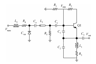
Fig. 1.
Schematic of Colpitts VCO designed in this paper.
SEMICONDUCTOR INTEGRATED CIRCUITS
Jincan Zhang1, Yuming Zhang2, Hongliang Lü2, , Yimen Zhang2, Bo Liu1, Leiming Zhang1 and Fei Xiang1
Corresponding author: Hongliang Lü, Email: hllv@mail.xidian.edu.cn
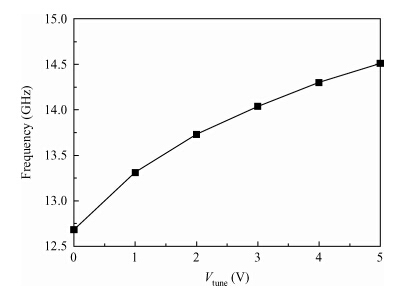
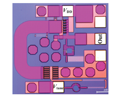
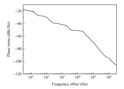
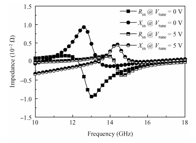
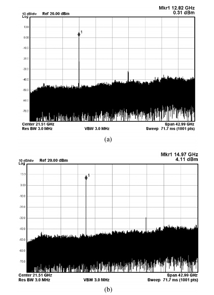
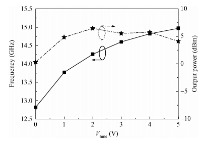
Abstract: A fully integrated Ku-band voltage controlled oscillator (VCO) is presented in an InGaP/GaAs heterojunction bipolar transistor (HBT) technology. To achieve the wide tuning range (TR), the VCO employs a Colpitts configuration, and the VCO simultaneously achieves high output power. The implemented VCO demonstrates an oscillation frequency range from 12.82 to 14.97 GHz, a frequency TR of 15.47%, an output power from 0.31 to 6.46 dBm, and a phase noise of-94.9 dBc/Hz at 1 MHz offset from 13.9 GHz center frequency. The VCO consumes 52.75 mW from 5 V supply and occupies an area of 0.81 × 0.78 mm2. Finally, the figures-of-merit for VCOs is discussed.
Keywords: voltage controlled oscillator, InGaP/GaAs HBT, Ku band, wide tuning range, high output power
| [1] | |
| [2] | |
| [3] | |
| [4] | |
| [5] | |
| [6] | |
| [7] | |
| [8] | |
| [9] | |
| [10] | |
| [11] | |
| [12] | |
| [13] | |
| [14] | |
| [15] |
| [1] | |
| [2] | |
| [3] | |
| [4] | |
| [5] | |
| [6] | |
| [7] | |
| [8] | |
| [9] | |
| [10] | |
| [11] | |
| [12] | |
| [13] | |
| [14] | |
| [15] |


Article views: 3213 Times PDF downloads: 33 Times Cited by: 0 Times
Received: 17 December 2014 Revised: Online: Published: 01 June 2015
| Citation: |
Jincan Zhang, Yuming Zhang, Hongliang Lü, Yimen Zhang, Bo Liu, Leiming Zhang, Fei Xiang. A Ku-band wide-tuning-range high-output-power VCO in InGaP/GaAs HBT technology[J]. Journal of Semiconductors, 2015, 36(6): 065010. doi: 10.1088/1674-4926/36/6/065010
****
J C Zhang, Y M Zhang, H Lü, Y M Zhang, B Liu, L M Zhang, F Xiang. A Ku-band wide-tuning-range high-output-power VCO in InGaP/GaAs HBT technology[J]. J. Semicond., 2015, 36(6): 065010. doi: 10.1088/1674-4926/36/6/065010.

|
| [1] | |
| [2] | |
| [3] | |
| [4] | |
| [5] | |
| [6] | |
| [7] | |
| [8] | |
| [9] | |
| [10] | |
| [11] | |
| [12] | |
| [13] | |
| [14] | |
| [15] |

 WeChat ID
Journal of Semiconductors © 2017 All Rights Reserved 京ICP备05085259号-2

 DownLoad: