Loading [MathJax]/jax/output/HTML-CSS/jax.js
J. Semicond. > 2015, Volume 36 > Issue 7 > 073006

SEMICONDUCTOR MATERIALS

Chemical and electrical properties of (NH4)2S passivated GaSb surface

Dongyan Tao, Yu Cheng, Jingming Liu, Jie Su, Tong Liu, Fengyun Yang, Fenghua Wang, Kewei Cao, Zhiyuan Dong and Youwen Zhao

+ Author Affiliations

 Corresponding author: Dongyan Tao, E-mail: dongyantao@semi.ac.cn

DOI: 10.1088/1674-4926/36/7/073006

PDF

Abstract: 
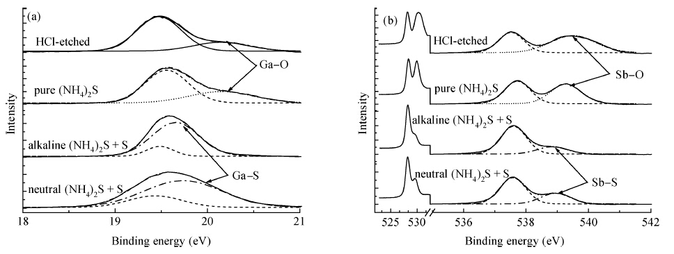
The surface chemical properties of gallium antimonide (GaSb) after ammonium sulfide ((NH4)2S) solution passivation have been studied by X-ray photoelectron spectroscopy (XPS), time of flight secondary ion mass spectroscopy (TOF-SIMS) and I-V measurement. An advantage of neutral (NH4)2S + S solution over pure (NH4)2S solution and alkaline (NH4)2S + S solution has been found in the ability to passivate the GaSb surface by contrast and comparison. It has been found that alkaline (NH4)2S + S solution passivation effectively removes oxides of the GaSb surface and forms sulfide products to improve device performance. TOF-SIMS complementally demonstrates that pure (NH4)2S passivation did form sulfide products, which are too soluble to really exist. The lowest roughness determined using a 3D optical profilometer and the highest improved SBD quality proved that neutral (NH4)2S + S solution passivation worked much better in improving the surface properties of GaSb.

Key words: surface passivationGaSbXPSTOF-SIMS

GaSb, which has a direct energy gap of 0.72 V, is the most suitable substrate in the epitaxial growth of mixed semiconductors of GaSb system, because of its small lattice mismatch[1, 2, 3]. GaSb-based devices are promising candidates for a variety of applications in infrared regimes, including infrared lasers, emitters and detectors[4, 5, 6]. Unfortunately, the high level of reverse current and surface instabilities deteriorates the performance and reliability of GaSb-based devices. Previous studies revealed that GaSb surface can be easily oxidized by atmospheric oxygen with the formation of native surface oxides several nanometers thick[7, \, 8]. Moreover, chemical processing of the GaSb surface is particularly difficult because of its high activity. Thurmond \textit{et al.}[9] showed that relevant reactions on GaSb yield interfacial deposits of Sb via 2GaSb + Sb2O3Ga2O3 + 4Sb. The excess Sb always acts as non-radiative center, leading to high surface recombination velocity and large leakage currents that hinder the enhancement of the device's performance. It is important to fabricate surfaces and interfaces with a low level of electronic states which means native surface oxides need to be prevented and processed as well as possible.

Much effort has been focused on GaSb crystal growth and device fabrications[10, 11]. The procedure of chemical preparation of the GaSb surface is still far from satisfactory. To our knowledge, sulfide passivation, using (NH4)2S solutions, has been performed extensively to reduce density of surface states and correspondingly lower dark current of mesa diodes[12]. However, the sulfide layer is slightly soluble, thus formation of sulfides is always unsatisfactory. To overcome this problem, excess sulfur (S) blended (NH4)2S solution and neutral (NH4)2S solution were studied to optimize the passivation effect. Generally, surface properties, including chemical components, roughness and electrical parameters, are important aspects to characterize the passivation effect. Moreover, changing relationship between these factors should also be considered. Thus, X-ray photoelectron spectroscopy (XPS) was applied to characterize GaSb surface information on chemical composition before and after passivation. Time of flight secondary ion mass spectroscopy (TOF-SIMS) and 3D surface topography were employed to detect chemical component variation and surface roughness. In particular, the impact of sulfide passivation on Au/n-GaSb Schottky junction behavior was studied. Excess S blended (NH4)2S solution improves the rectifying behavior and reduces the reverse current more obviously. The purpose of this study is to evaluate surface properties of GaSb surface passivated by different (NH4)2S solutions. Additionally, the effect of hydrogen in (NH4)2S solution on the passivation reaction is also discussed.

Te-doped n-type GaSb (n= 1.3 × 1017 cm3, μ = 2446~cm2/(Vs), T= 300 K) two side polished substrate with 500 μm thick was used in this study. Prior to further treatment, all samples were cleaned by standard surface cleaning steps consisting of degreasing in acetone, alcohol, and DI water in order to remove organic contamination. We labeled the treated samples as samples (a)-(d).

(a) Dipped in concentrated HCl solution for 5 min;

(b) Dipped in concentrated HCl solution for 5 min, and then sulfured by soaking in pure (NH4)2S solution for 5 min;

(c) Dipped in concentrated HCl solution for 5 min, and then sulfured by soaking in alkaline (NH4)2S + S solution for 5~min at 60 C. The alkaline (NH4)2S + S solution was prepared by dissolving 2 g sulfur in 100 mL pure (NH4)2S solution;

(d) Dipped in concentrated HCl solution for 5 min, and then sulfured by soaking in neutral (NH4)2S + S solution for 5~min at 60 C. The pH value of alkaline (NH4)2S + S solution turned to 7 by dipping HCl, referred to as neutral (NH4)2S + S solution.

Finally, all treated samples were dried by nitrogen gas flow, and then sealed in sample boxes protected by nitrogen prior to XPS and TOF-SIMS measurements. XPS was carried out in a Kratos Axis-165 system using a monochromated Al source under ultra-high vacuum (base pressure 5 × 10⁷~mTorr). All XPS scans were done at room temperature with 0.1 eV step size, 30 ms dwell time, and no additional \textit{in situ} processing. TOF-SIMS analysis was carried out with a TOF-SIMS V instrument from ION-TOF. Surface roughness was characterized using a 3D optical profilometer (ContourGT-K1, Bruker, Germany). Images were recorded at three different locations on each sample using the 3D profilometer to obtain the average value of surface roughness. The semiconductor parameter analyzer (Agilent B1500) was observed to evaluate sulphurization effects on electrical transport properties of Au/n-GaSb Schottky diode. Circular Au Schottky contact, Φ = 0.50 mm, 100 nm thick, was resistively evaporated through a metal shadow mask. Rear-side Ohmic contact was made by evaporating AuGeNi and then alloyed at 280 C for 2 min.

Figure 1 shows typical room temperature Ga 3d and Sb 3d doublet spectra obtained from the GaSb surface. Background subtraction and iterative lineshape decomposition based on the Gaussian function were performed to analyze the core level spectra. Sb 3d3/2 was analyzed instead of Sb 3d5/2, because the signal peaks of Sb 3d5/2 in XPS spectra almost overlap with O 1s.

Figure  1.  XPS (a) Ga 3d and (b) Sb 3d spectra and simulation results obtained from HCl-etched (sample (a)), pure (NH4)2S solution passivation (sample (b)), alkaline (NH4)2S + S solution passivation (sample (c)) and neutral (NH4)2S + S solution passivation (sample (d)).

As shown in Figure 1(a), peaks due to oxides of Ga were detected from samples (a) and (b) at a binding energy of 20.6~eV. The position and intensity of Ga-O signal changed little after pure (NH4)2S solution passivation. However, it was drastically reduced after alkaline (NH4)2S + S solution passivation. A new component at a binding energy of 19.8 eV became visible due to formation of Ga-S bonds. This was verified by the argument that chemical shifts are mainly due to charge transfer[13]. Indeed, the Pauling electro-negativities for Ga, O and S are 1.8, 3.5 and 2.5, respectively. The binding energy of Ga-S compound is thus expected to be between that of Ga0 and Ga-O bond. Although determination of the exact composition of this component is difficult, judging from Pauling electro-negativities difference, it is definitely Ga-S bonds. The intensity and relative area ratio of Ga-S bonds has been increased after the GaSb surface was subjected to neutral (NH4)2S + S solution passivation. It was clearly shown in Figure 1(b), Sb 3d3/2 spectra were deconvoluted into Sb-Ga and Sb-O bonds from samples (a) and (b). The relative area ratio of Sb-O to Sb-Ga bonds from sample (b) decreased compared to that from sample (a). After alkaline (NH4)2S + S solution passivation, the core level line of Sb-O disappeared and a new peak at binding energy of 538.8 eV can be readily identified to be Sb-S bonds. Just like the case in Ga-S bonds, the formation and intensity of Sb-S bonds became more apparent after neutral (NH4)2S + S solution passivation. The result of passivated surfaces suggests that sulfur agent dissolves native oxide present on the semiconductor surface and forms S-S, S-Ga, and S-Sb bonds in the surface layer. The formation of these bonds causes a reduction in the density of surface states. Considering the fact that sulfide products should exist on the GaSb surface after pure (NH4)2S solution passivation, the absence of Ga-S/Sb-S bonds from sample (b) demonstrates that sulfide products are unstable, or soluble, in pure (NH4)2S solution. Alkaline (NH4)2S + S solution goes through the following reactions[14]:

S+OHS+2SO23+H2O(60C), (1)
S2+H2OHS+OH, (2)
NH+4+HSNH4SH, (3)
GaxOy+NH4SH+H2OGaxSy+NH4OH+H2, (4)
SbxOy+NH4SH+H2OSbxSy+NH4OH+H2. (5)

Thus, excess sulfur in alkaline (NH4)2S + S solution can increase the amount of sulfide products. The achieved thicker sulfide layer in neutral (NH4)2S + S solution clearly confirms that neutral (NH4)2S + S solution passivation is more effective to remove oxides and form thicker sulfides layer on the GaSb surface. The additional hydrogen ions condition shifts the equilibrium of reactions (4) and (5) to the right. The preferential replacement of sulfides with their corresponding oxides can be explained by Pearson acid-base concept[15].

Spectra in Figure 2 obtained by TOF-SIMS confirm that oxide-related peaks such as Ga2O3 and Sb2O3 are detected in sample (a), which are attributed to the nature of the GaSb surface. Besides, the appearance of Sb signals in Figure 2(a)-pos, which are not detected in XPS measurement due to the detection limit, partially clarified the origin of the reverse current. Due to pure (NH4)2S solution passivation (sample (b)), the amount of oxides and excess Sb decreased, promoting the enhancement of the device's performance. Meanwhile, signals of GaS and SbS in Figure 2(b) revealed that there were some sulfide products on the GaSb surface after pure (NH4)2S solution passivation, which is in good agreement with our XPS assumption and analysis.

Figure  2.  Comparison of TOF-SIMS positive (-pos) and negative (-neg) mass spectrum obtained from (a) HCl-etched (sample (a)) and (b) pure (NH4)2S solution passivation (sample (b)). The unmarked peak positions are caused by the isotope of Ga and/or Sb, which are not considered during the analysis.

Figure 3 depicts surface topography for four respective treated GaSb samples. The surface of sample (a) is rather irregular and contains a multitude of, what appears to be, etching related corrosion areas. Samples (b), (c) and (d), however, appear smoother with smaller roughness value, suggesting more or less uniform passivation of the surface. Table 1 lists the results of surface roughness recorded at three different locations on each sample. The corrosion areas appear to be relatively shallow with roughness of 0.521 nm after pure (NH4)2S solution passivation. However, the smooth corrosion area is destabilized during alkaline (NH4)2S + S solution exposure to 60~C. Passivation reactions continue at a rapid speed, resulting in increased surface roughness, 0.570 nm. In the case of neutral (NH4)2S + S solution, thicker sulfides can be formed due to the repression of sulfide solubility. The corrosion area can cease to passivate beyond a certain thickness, resulting in a flat surface with the lowest roughness, 0.486 nm.

Figure  3.  Surface topography for HCl-etched (sample (a)), pure (NH4)2S solution passivation (sample (b)), alkaline (NH4)2S + S solution passivation (sample (c)) and neutral (NH4)2S + S solution passivation (sample (d)).
Table  1.  The results of surface roughness recorded at three different locations on each sample.
DownLoad: CSV  | Show Table

To further understand the detailed information of (NH4)2S sulfide passivation on the GaSb surface, representative I-V characteristics under forward and reverse biases are shown in Figure 4. The Schottky diode made on neutral (NH4)2S + S solution passivation exhibited the highest improved SBD quality, as evidenced by strongly reduced reverse currents and relative high rectification ratio. These observations combined with the above XPS and TOF-SIMS analysis suggested that electronic states density, as well as excess Sb on the GaSb surface which contributes to reverse current, decreases efficiently after neutral (NH4)2S + S solution passivation.

Figure  4.  I-V characteristics of Au/n-GaSb Schottky contacts under forward and reverse bias.

In this paper, we have investigated surface chemical properties of (NH4)2S passivation of the GaSb surface by XPS. Although pure (NH4)2S solution passivation did form sulfides, it has less obvious effect on the reduction of surface states due to the solubility of sulfide products. On the other hand, attributed to excess sulfur, alkaline (NH4)2S + S solution passivation proved to be better as justified from the appearance of Ga-S and Sb-S bonds from XPS analysis. Moreover, both TOF-SIMS and surface topography measurement confirm that neutral (NH4)2S + S solution passivation is more effective in forming a thicker sulfide layer with higher stability than the alkaline one. I-V characteristic upon it exhibited the most significant reduction in surface states and improvement in device performance. In conclusion, neutral (NH4)2S + S solution passivation is proved to be more effective in improving surface properties of GaSb compared to pure (NH4)2S solution and alkaline (NH4)2S + S solution. We attribute this to the promoted effect of additional hydrogen ions in neutral (NH4)2S + S solution which shifts the equilibrium of passivation reactions to the right.


[1]
[2]
[3]
[4]
[5]
[6]
[7]
[8]
[9]
[10]
[11]
[12]
[13]
[14]
[15]
Fig. 1.  XPS (a) Ga 3d and (b) Sb 3d spectra and simulation results obtained from HCl-etched (sample (a)), pure (NH4)2S solution passivation (sample (b)), alkaline (NH4)2S + S solution passivation (sample (c)) and neutral (NH4)2S + S solution passivation (sample (d)).

Fig. 2.  Comparison of TOF-SIMS positive (-pos) and negative (-neg) mass spectrum obtained from (a) HCl-etched (sample (a)) and (b) pure (NH4)2S solution passivation (sample (b)). The unmarked peak positions are caused by the isotope of Ga and/or Sb, which are not considered during the analysis.

Fig. 3.  Surface topography for HCl-etched (sample (a)), pure (NH4)2S solution passivation (sample (b)), alkaline (NH4)2S + S solution passivation (sample (c)) and neutral (NH4)2S + S solution passivation (sample (d)).

Fig. 4.  I-V characteristics of Au/n-GaSb Schottky contacts under forward and reverse bias.

Table 1.   The results of surface roughness recorded at three different locations on each sample.

DownLoad: CSV
[1]
[2]
[3]
[4]
[5]
[6]
[7]
[8]
[9]
[10]
[11]
[12]
[13]
[14]
[15]
1

Interfacial dynamics of GaP/Si(100) heterostructure grown by molecular beam epitaxy

Tieshi Wei, Xuefei Li, Zhiyun Li, Wenxian Yang, Yuanyuan Wu, et al.

Journal of Semiconductors, 2022, 43(12): 122101. doi: 10.1088/1674-4926/43/12/122101

2

Performance enhancement of solution-processed InZnO thin-film transistors by Al doping and surface passivation

Wensi Cai, Haiyun Li, Mengchao Li, Zhigang Zang

Journal of Semiconductors, 2022, 43(3): 034102. doi: 10.1088/1674-4926/43/3/034102

3

Rational molecular passivation for high-performance perovskite light-emitting diodes

Jingbi You

Journal of Semiconductors, 2019, 40(4): 040203. doi: 10.1088/1674-4926/40/4/040203

4

Surface passivation of perovskite film for efficient solar cells

Yang (Michael) Yang

Journal of Semiconductors, 2019, 40(4): 040204. doi: 10.1088/1674-4926/40/4/040204

5

Boron-rich layer removal and surface passivation of boron-doped p–n silicon solar cells

Caixia Hou, Rui Jia, Ke Tao, Shuai Jiang, Pengfei Zhang, et al.

Journal of Semiconductors, 2018, 39(12): 122004. doi: 10.1088/1674-4926/39/12/122004

6

Improved interfacial properties of GaAs MOS capacitor with NH3-plasma-treated ZnON as interfacial passivation layer

Jingkang Gong, Jingping Xu, Lu Liu, Hanhan Lu, Xiaoyu Liu, et al.

Journal of Semiconductors, 2017, 38(9): 094004. doi: 10.1088/1674-4926/38/9/094004

7

The effect of nitridation and sulfur passivation for In0.53Ga0.47As surfaces on their Al/Al2O3/InGaAs MOS capacitors properties

Zizeng Lin, Mingmin Cao, Shengkai Wang, Qi Li, Gongli Xiao, et al.

Journal of Semiconductors, 2016, 37(2): 026002. doi: 10.1088/1674-4926/37/2/026002

8

Effective interface passivation of a Ge/HfO2 gate stack using ozone pre-gate treatment and ozone ambient annealing

Mei Zhao, Renrong Liang, Jing Wang, Jun Xu

Journal of Semiconductors, 2013, 34(6): 066005. doi: 10.1088/1674-4926/34/6/066005

9

Influence of the Annealing Temperature on the Structural and Optical Properties of N-Doped ZnO Films

Zhong Sheng, Xu Xiaoqiu, Sun Lijie, Lin Bixia, Fu Zhuxi, et al.

Journal of Semiconductors, 2008, 29(7): 1330-1333.

10

A Transition Region Study of SiO2/4H-SiC Interface by ADXPS

Wang Dejun, Zhao Liang, Zhu Qiaozhi, Ma Jikai, Chen Suhua, et al.

Journal of Semiconductors, 2008, 29(5): 944-949.

11

XPS of SiCN Thin Films Prepared by C+ Implantation in Amorphous SiNx∶H

Chen Chao, Liu Yuzhen, Dong Lijun, Chen Dapeng, Wang Xiaobo, et al.

Chinese Journal of Semiconductors , 2007, 28(3): 415-419.

12

GaSb Bulk Materials and InAs/GaSb Superlattices Grown by MBE on GaAs Substrates

Hao Ruiting, Xu Yingqiang, Zhou Zhiqiang, Ren Zhengwei, Niu Zhichuan, et al.

Chinese Journal of Semiconductors , 2007, 28(7): 1088-1091.

13

Lattice Perfection of GaSb and InAs Single Crystal Substrate

Lü Xiaohong, Zhao Youwen, Sun Wenrong, Dong Zhiyuan

Chinese Journal of Semiconductors , 2007, 28(S1): 163-166.

14

Analysis of PTCDA/ITO Surface and Interface Using X-ray Photoelectron Spectroscopy and Atomic Force Microscopy

Ou Guping, Song Zhen, Gui Wenming, Zhang Fujia

Chinese Journal of Semiconductors , 2006, 27(2): 229-234.

15

AFM and XPS Study on the Surface and Interface States of CuPc and SiO2 Films

Chen Jinhuo, Wang Yongshun, Zhu Haihua, Hu Jiaxing, Zhang Fujia, et al.

Chinese Journal of Semiconductors , 2006, 27(8): 1360-1366.

16

Effect of Ion Energy and Substrate Temperature on Gadolinium Oxide Structure

Zhou Jianping, Chai Chunlin, Yang Shaoyan, Liu Zhikai, Song Shulin, et al.

Chinese Journal of Semiconductors , 2005, 26(S1): 57-60.

17

CH3CSNH2/NH4OH Passivation on GaInAsSb/GaSb PIN Infrared Photodetectors

Liu Yanxiang, Tang Shaoqiu, Xia Guanqun, Cheng Zongquan, Zheng Yanlan, et al.

Chinese Journal of Semiconductors , 2005, 26(S1): 132-135.

18

Growth and Characterisation of InAsSb Ternary Layers on (101) GaSb Substrates by LP-MOCVD

Li Xiaoting, Wang Tao, Wang Jingwei, Wang Yiding, Yin Jingzhi, et al.

Chinese Journal of Semiconductors , 2005, 26(12): 2298-2302.

19

用TOF-SIMS研究半导体芯片铝键合点上的有机沾污

Chinese Journal of Semiconductors , 1998, 19(9): 702-706.

20

a-Si:(H,Cl)薄膜的XPS和UPS研究

Chinese Journal of Semiconductors , 1983, 4(6): 590-592.

1. Hao, L., He, G., Jiang, S. et al. Fermi level unpinning achievement and transport modification in Hf1-xYbxOy/Al2O3/GaSb laminated stacks by doping engineering. Journal of Materials Science and Technology, 2022. doi:10.1016/j.jmst.2022.02.010
2. Devaray, P., Hatta, S.F.W.M., Wong, Y.H. An overview of conventional and new advancements in high kappa thin film deposition techniques in metal oxide semiconductor devices. Journal of Materials Science: Materials in Electronics, 2022. doi:10.1007/s10854-022-07975-7
3. Hao, L., He, G., Zheng, G. et al. Interface Optimization and Modulation of Leakage Current Conduction Mechanism of Yb2O3/GaSb MOS Capacitors with ALD-Driven Laminated Interlayers. ACS Applied Electronic Materials, 2021, 3(2): 872-881. doi:10.1021/acsaelm.0c00988
4. Hao, L., He, G., Qiao, L. et al. Interface Optimization and Modulation of Leakage Current Conduction Mechanism of Yb2O3/GaSb MOS Capacitors with (NH4)2S Solutions Passivation. IEEE Electron Device Letters, 2021, 42(2): 140-143. doi:10.1109/LED.2020.3048014
5. Su, J., Liu, T., Liu, J. et al. Electrical and optical property of annealed Te-doped GaSb. Journal of Semiconductors, 2017, 38(4): 043001. doi:10.1088/1674-4926/38/4/043001
  • Search

    Advanced Search >>

    GET CITATION

    Dongyan Tao, Yu Cheng, Jingming Liu, Jie Su, Tong Liu, Fengyun Yang, Fenghua Wang, Kewei Cao, Zhiyuan Dong, Youwen Zhao. Chemical and electrical properties of (NH4)2S passivated GaSb surface[J]. Journal of Semiconductors, 2015, 36(7): 073006. doi: 10.1088/1674-4926/36/7/073006
    D Y Tao, Y Cheng, J M Liu, J Su, T Liu, F Y Yang, F H Wang, K W Cao, Z Y Dong, Y W Zhao. Chemical and electrical properties of (NH4)2S passivated GaSb surface[J]. J. Semicond., 2015, 36(7): 073006. doi: 10.1088/1674-4926/36/7/073006.
    shu

    Export: BibTex EndNote

    Article Metrics

    Article views: 2507 Times PDF downloads: 20 Times Cited by: 5 Times

    History

    Received: 28 September 2014 Revised: Online: Published: 01 July 2015

    Catalog

      Email This Article

      User name:
      Email:*请输入正确邮箱
      Code:*验证码错误
      Dongyan Tao, Yu Cheng, Jingming Liu, Jie Su, Tong Liu, Fengyun Yang, Fenghua Wang, Kewei Cao, Zhiyuan Dong, Youwen Zhao. Chemical and electrical properties of (NH4)2S passivated GaSb surface[J]. Journal of Semiconductors, 2015, 36(7): 073006. doi: 10.1088/1674-4926/36/7/073006 ****D Y Tao, Y Cheng, J M Liu, J Su, T Liu, F Y Yang, F H Wang, K W Cao, Z Y Dong, Y W Zhao. Chemical and electrical properties of (NH4)2S passivated GaSb surface[J]. J. Semicond., 2015, 36(7): 073006. doi: 10.1088/1674-4926/36/7/073006.
      Citation:
      Dongyan Tao, Yu Cheng, Jingming Liu, Jie Su, Tong Liu, Fengyun Yang, Fenghua Wang, Kewei Cao, Zhiyuan Dong, Youwen Zhao. Chemical and electrical properties of (NH4)2S passivated GaSb surface[J]. Journal of Semiconductors, 2015, 36(7): 073006. doi: 10.1088/1674-4926/36/7/073006 ****
      D Y Tao, Y Cheng, J M Liu, J Su, T Liu, F Y Yang, F H Wang, K W Cao, Z Y Dong, Y W Zhao. Chemical and electrical properties of (NH4)2S passivated GaSb surface[J]. J. Semicond., 2015, 36(7): 073006. doi: 10.1088/1674-4926/36/7/073006.

      Chemical and electrical properties of (NH4)2S passivated GaSb surface

      DOI: 10.1088/1674-4926/36/7/073006
      Funds:

      Project supported by the National Natural Science Foundation of China (No. 61474104).

      More Information
      • Corresponding author: E-mail: dongyantao@semi.ac.cn
      • Received Date: 2014-09-28
      • Accepted Date: 2015-02-02
      • Published Date: 2015-01-25

      Catalog

        /

        DownLoad:  Full-Size Img  PowerPoint
        Return
        Return