Processing math: 100%
J. Semicond. > 2015, Volume 36 > Issue 8 > 084006

SEMICONDUCTOR DEVICES

ZnO/Ag nanowires composite film ultraviolet photoconductive detector

Guodong Yan, Minqiang Wang and Zhi Yang

+ Author Affiliations

 Corresponding author: Minqiang Wang, Email: mqwang@mail.xjtu.edu.cn

DOI: 10.1088/1674-4926/36/8/084006

PDF

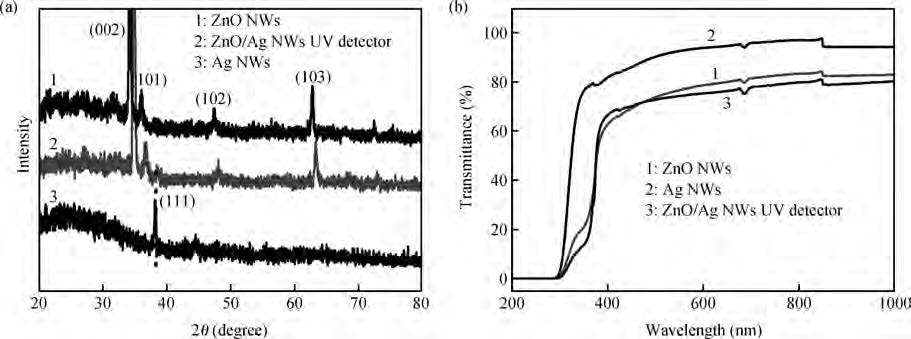
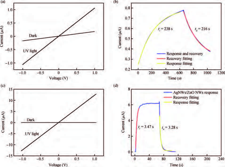
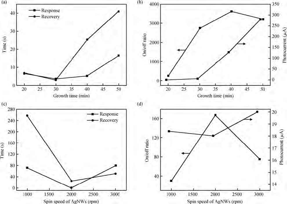
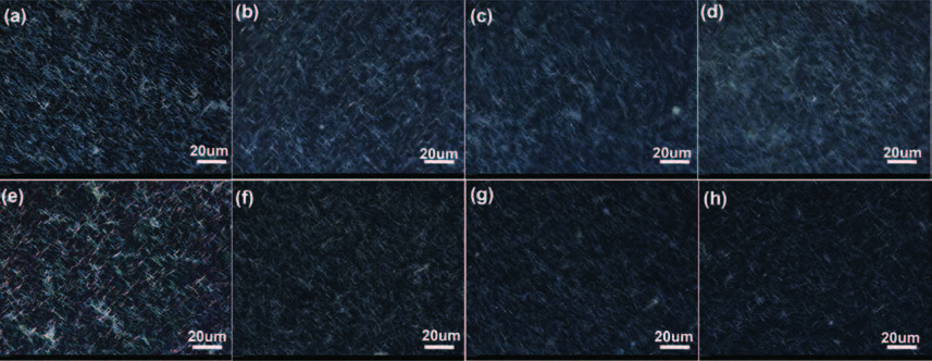
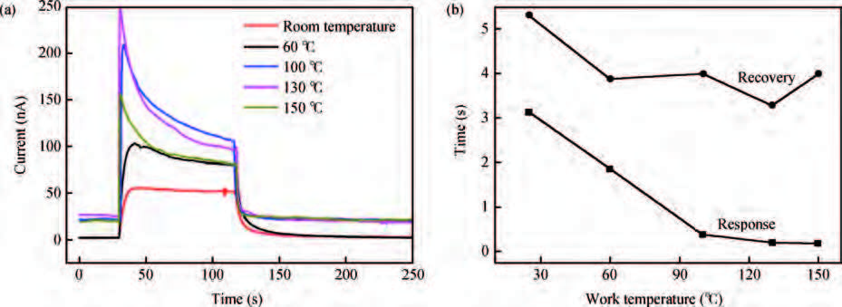
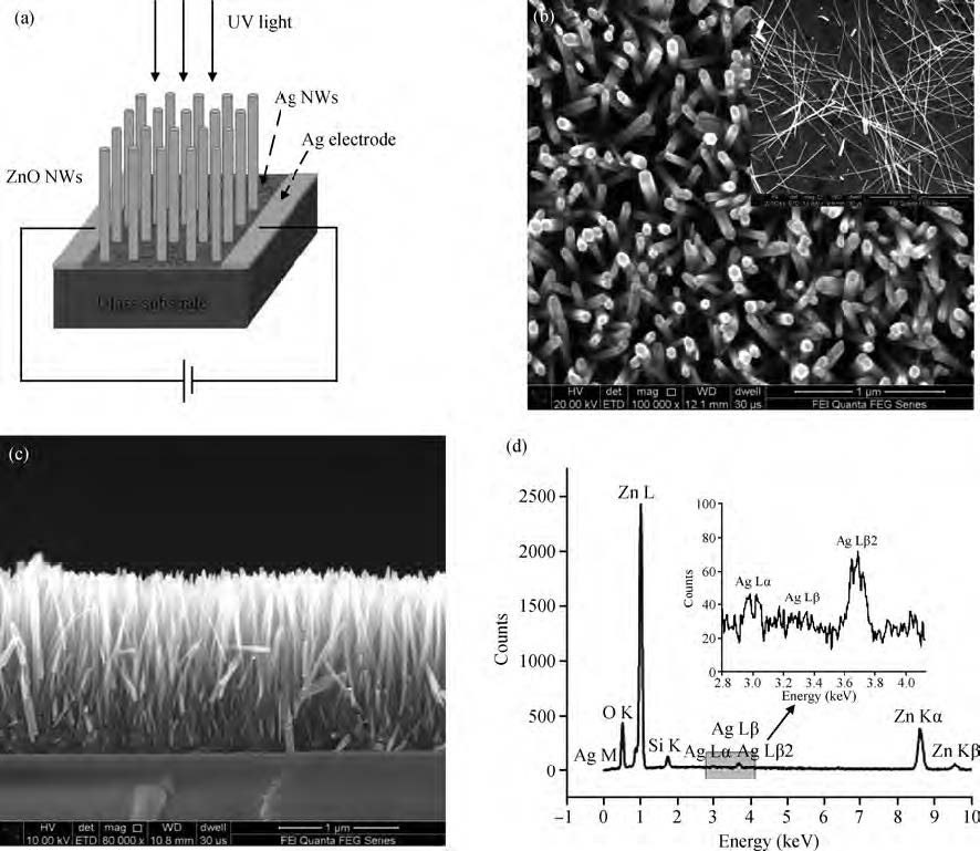
Abstract: ZnO/Ag nanowires (NWs) film ultraviolet (UV) detector was fabricated by a simple and low-cost solution-processed method. In order to prepare this device, Ag NWs network was first spin-coated on glass substrate as a transparent conducting electrode, then ZnO NWs arrays were grown vertically on the Ag NWs network based on the hydrothermal method. This UV detector exhibited an excellent detection performance with large on/off ratio and short response time. Several process and working parameters were particularly investigated to analyze the relationship between structure and performance, which include growth time of ZnO NWs array, spin speed of Ag NWs network and working temperature. This UV photoconductive detector is based on two kinds of one-dimension nanomaterials, and it was regarded as a compromise between high performance with large area, low voltage and low cost.

Key words: UV detectorZnO NWs arrayAg NWs

The UV detector has become a hot research field for several years due to its wide application range in civilian and military fields. For instance,the UV detector can be used for environmental monitoring,missile launching detection,space research and high temperature flame detection,and so on[1]. High on/off ratio,fast response and recovery speed are the common requirement of a UV detector[2]. Compared with the Si-based UV detector and the GaN-based UV detector[1, 3, 4],the ZnO-based UV detector has a lot of advantages,such as room-temperature operation,low-temperature synthesis,chemical stability,abundant raw materials. In addition,ZnO is a wide-direct-gap semiconductor with a high excitation energy of 60 meV and bandgap energy of 3.37 eV at room temperature[5, 6, 7],so ZnO has been widely used in UV detectors. Due to the large surface-to-volume ratio and reduced dimensionality of the active area in ZnO NWs,the ZnO NWs UV detector has high photoconductive gain[1]. In Wang's research,the gain of the ZnO NWs UV detector is about 108[1]. However,persistent photoconductivity (PPC) phenomenon on the surface of ZnO leads to the long response and recovery time in the ZnO NWs UV detector[8]. According to Ji's research,the recovery time of the ZnO NWs UV detector is about 15 s,which is bad for the application of the ZnO NWs UV detector[8].

As one-dimensional conductive nanomaterials,Ag NWs networks film has high transmittance and excellent conductivity,which can partly improve the photoconductive gain and shorten the response and recovery time as transparent electrode[9]. In the ZnO NWs-based UV detector,Ag NWs can quickly transfer photoelectrons and prevent recombination of photoelectrons and holes[10, 11]. At the same time,the ZnO/Ag NWs film is also a favorable kind of transparent conductive electrode,the photoelectron can be transferred easily in the composite film[12].

In this paper,the ZnO/Ag NWs UV detector,which is ZnO-Ag nanowire heterostructure,has been fabricated according to the process described in the following experimental details. In this UV detector,ZnO NWs are used to absorb UV light and generate photoelectrons and holes,Ag NWs can quickly transfer photoelectrons to the external circuit. Many measurements have been done for characterizing the performance of the ZnO/Ag NWs UV detector under different processing conditions,for example I-V characteristics,and response and recovery characteristics. The results show that the ZnO/Ag NWs UV detector with a large area of 10 × 8 mm2 has a good performance. Besides,the preparation process and working condition of this UV detector have been optimized to obtain the best UV detection performance.

Ag NWs were synthesized by polyol method as follows. 166.5 mg of polyvinyl pyrrolidone (PVP,Mw = 40000) and 170 mg of silver nitrate (AgNO3) were dissolved in 10 mL of ethylene glycol (EG). AgNO3 solution gradually changed from transparent to burgundy after sonication for 7 min. 800 μL of 1 mM ferric chloride (FeCl3) solution was added to 9.2 mL of EG and stirred for 3 min. Then the AgNO3 solution was added to FeCl3 solution at a rate of 0.4 mL/min,and stirred for 3 min. The mixed solution was heated at 150 for 40 min in air atmosphere. The cooled down solution was washed with ethanol to remove solvents (EG),PVP and other impurities by successive rounds of centrifugation and removal of the supernatant. Finally,the washed Ag NWs were dispersed in 4 mL of ethanol or methanol and stored at the room temperature.

Colloidal ZnO nanoparticles (NPs) were synthesized by hydrolyzing zinc acetate dihydrate (Zn(AC)2) in methanol solution[13]. 0.818 g of Zn(AC)2 was first dissolved in 42 mL of methanol. 0.4859 g of potassium hydroxide (KOH) was first dissolved in 23 mL of methanol. 42 mL of Zn(AC)2 solution was added to KOH solution at a rate of 4 mL/min. This mixed solution was aged at 60 with stirring and refluxing for 2 h. To purify this ZnO NPs,the solution is centrifuged twice at 4800 rpm for 30 min. Then the ZnO precipitate was redispersed in methanol by sonication dispersion method.

Ag NWs ethanol solution was deposited onto the glass substrate by spin coating. Ag NWs film was annealed at 220 for 30 min in order to decrease the contact resistance. A silver paste pad served as an electrode for this device. Ag NWs deposited on glass substrate were dropped with 30 μL of ZnO NPs methanol solution to form a ZnO seed layer. The seed sample was annealed at 300 for 30 min to increase the seed layer adhesion. Then seed sample was dipped into the growth solution at 83 ,which contains 0.8 g of sodium hydroxide (NaOH) and 0.295 g of zinc nitrate hexahydrate (Zn(NO3)26(H2O)).

The morphologies of samples were characterized by an FEI Quantan 250 FEG scanning electron microscope (SEM) equipped with X-ray energy dispersive spectrometer (EDS). The low magnification image of the UV detector was taken with Olympus BX51 microscope system. The phase composition and crystal structure of the UV detector were determined by a D/max-2400 diffractometer (Rigaku,Japan). Optical transmittance and absorptance spectra were recorded with a Jasco-V570 UV-vis-NIR spectrophotometer. I-V- and time-dependent photoresponse measurements were performed with a Keithley 2400 source meter upon the illumination of a mercury lamp (Starsense,GGY-125). The UV light intensity was quantified by a standard silicon diode UV of 365 nm (Photoelectric Instrument Factory of Beijing Normal University,UV-A)

Figure 1(a) shows the schematic structure of the ZnO/Ag NWs UV detector. Ag electrodes directly connect with Ag NWs film to form a conductive network,and Ag NWs are covered with ZnO seed layer except for the regions of Ag electrodes. Then the ZnO NWs arrays grow on the ZnO seed layer. In the ZnO/Ag NWs UV detector,ZnO NWs absorb UV light and generate photoelectrons and holes; Ag NWs are used to transfer photoelectrons and prevent the recombination of photoelectrons and holes. The insert of Figure 1(b) is the SEM image of Ag NWs network. From the image,it can be clearly seen that the average diameter and length of Ag NWs are about 80 nm and 20 μm,respectively. Besides,the uniform nanowires network can result in high conductivity and transmittance of Ag NWs film. Figures 1(b) and 1(c) are the SEM images of top and cross-section view of the ZnO/Ag NWs UV detector,respectively. It can be seen that the ZnO NWs with high density grow on the Ag NWs network vertically,which has the diameter of 100 nm and the length of 1.5 μm. Unfortunately,the bottom layer Ag NWs cannot be seen clearly in the SEM images due to good conductive ZnO and far lower density of Ag NWs compared with ZnO NWs. However,the cross section of the ZnO/Ag NWs UV detector is analyzed by EDS spectra to further confirm the existence of the bottom layer Ag NWs. The characteristic peaks of Ag are clearly shown in the insert of Figure 1(d). In addition,the XRD pattern of the ZnO/Ag NWs UV detector also indicates the existence of Ag NWs in the UV detector. In Figure 6(d),Ag NWs of this UV detector with the optical microscope image can be clearly seen. The above results can identify the Ag NWs at the bottom of the ZnO/Ag NWs UV detector.

Figure  1.  (a) Schematic of the ZnO/Ag NWs UV detector structure. (b) Top and (c) cross section view of the ZnO/Ag NWs UV detector, the insert in (b) is surface morphologies of Ag NWs. (d) The EDS spectra of the cross section of the ZnO/Ag NWs UV detector, the insert shows the EDS spectra of the bottom layer Ag NWs clearly.

Figure 2(a) shows the XRD pattern of the ZnO NWs,Ag NWs and ZnO/Ag NWs UV detector. For the Ag NWs film,the peaks can be indexed to the face-center-cubic structure,and the strongest peak (111) indicates Ag NWs grow along the (111) direction[14]. In the case of ZnO NWs,the four peaks (002),(101),(102),(103) can be indexed to hexagonal wurtzite ZnO structure (JCPDS: 36-1451). The XRD pattern of the ZnO/Ag NWs UV detector shows the peaks of both ZnO and Ag NWs. Due to the majority amount of ZnO NWs in the UV detector,the peak of Ag NWs is relatively weak. The transmittance at 550 nm is usually used to evaluate the visible transmittance ability of transparent film[9]. As shown in Figure 2(b),the transmittance of the Ag NWs film,ZnO NWs and composite ZnO/Ag NWs film are 92%,77% and 74% at 550 nm,respectively. The superior transmittance of Ag NWs network and ZnO layer in visible and IR wavelength can result in good transmittance of the ZnO/Ag NWs UV detector. In particular,the transmittance of both the ZnO NWs and ZnO/Ag NWs detector has a significant decrease from 400 nm due to intrinsic absorption of ZnO NWs.

Figure  2.  (a) The XRD pattern of ZnO NWs array, Ag NWs film and ZnO/Ag NWs UV detector. (b) The transmittance spectrum of ZnO NWs array, Ag NWs film and ZnO/Ag NWs UV detector.

The basic working mechanism of the ZnO/Ag NWs UV detector is shown in Figure 3. Figure 3(a) shows oxygen molecules are absorbed on the surface of ZnO NWs in the dark,which can capture free electrons to form a low conductivity depletion layer[15]. (O2(g) + e O2(ad)) The photoresponse process of the detector upon UV illumination is shown in Figure 3(b). The electron-hole pairs are generated upon UV illumination. (hvh+ + e) The photo-generated holes migrate to the depletion and neutralize the negatively charged oxygen ions. Consequently,oxygen is desorbed from the surface of ZnO[2]. (h+ + O2(ad) O2(g)) The photocurrent increases rapidly because a large number of unpaired electrons are released upon UV illumination[1, 8, 11]. Besides,a pair of water molecules,which are dissociated by establishing a hydrogen bond and adsorbed on the surface of ZnO NWs,can capture both electron and hole upon UV illumination[16,\,17]. This process will decrease the carrier density and create a depletion layer near ZnO NWs surface,resulting in photocurrent decreases during UV illumination[18]. So the photocurrent of this UV detector gradually decreases in the wet air. As shown in Figure 3(c),the electron and hole will recombine again when UV illumination is off. The absorbed oxygen molecules capture these extra electrons within ZnO NWs. (O2(g) + e O2(ad)) Figure 3(d) shows that only oxygen molecules absorb on ZnO NWs surface,but water molecules no longer exist on ZnO NWs surface because of high temperature. A lot of electrons and holes,which dissociate the water molecules,are released from the ZnO NWs surface. The photocurrent increases at high temperature compared to the photocurrent of the UV detector at room temperature.

Figure  3.  (Color online) The schematic of the photoresponse process of the ZnO/Ag NWs UV detector. (a) Dark state. (b) Under UV illumination at room temperature. (c) Recovery to dark state. (d) Upon UV illumination at high temperature. (e) Energy level diagram of ZnO and Ag. (f) Schematic of the metastable state absorbing oxygen molecules.

Figure 3(e) shows the energy level diagram of ZnO-Ag heterojunction. Since the work function of ZnO NWs (5.25 eV) is higher than that of Ag NWs (4.26 eV),electrons in Ag NWs would move to the conduction band (CB) of ZnO to achieve the Fermi level equilibration,and then ZnO-Ag heterojunction is formed. When ZnO/Ag NWs UV detector is illuminated by UV light,electrons can be excited from valance band (VB) to conduction band (CB),and the same amount of holes are simultaneously generated and left in VB. The photoelectrons can quickly transfer to Ag NWs in order to prevent the photoelectrons and holes recombination,so the lifetime of photoelectrons and holes are prolonged. Figure 3(f) explains the reason for the PPC phenomenon of ZnO in the UV detector. The explanation of PPC phenomenon is following,electrical conductivity of ZnO will persistently increase upon UV illumination and last for some time even in the absence of UV illumination[19]. The origin of ZnO PPC phenomenon in the photodetector systems is still a controversial issue. The essence of PPC phenomenon is the defects in metastable charge states. Some electrons are trapped in the metastable state,and the oxygen molecule is slowly re-adsorbed on the surface of ZnO. So PPC phenomenon is likely to appear,make the energy band bend[15, 20] and prolong the response and recovery time of the ZnO photodetector.

Figures 4(a) and 4(c) are I-V curves of the ZnO NWs and ZnO/Ag NWs UV detector with and without UV illumination,respectively. The linear relationship between current and voltage of the ZnO/Ag NWs UV detector indicates good ohmic contact between the ZnO NWs array and Ag NWs[21]. The dark current and the photocurrent are 0.004 μA and 12.8 μA at 1 V applied bias upon the 365 nm UV illumination,respectively. So the on/off ratio is about 3100. Compared with the ZnO/Ag NWs UV detector,the dark current of the ZnO NWs UV detector is 0.16 μA,the photocurrent is 0.96 μA,so the on/off ratio is calculated as 6. Figures 4(b) and 4(d) show response and recovery characteristics of the ZnO NWs and ZnO/Ag NWs UV detector,respectively. The response and recovery data can be obtained by fitting the experimental curve with an exponential function. The response and recovery times of the ZnO NWs UV detector are 238 s and 216 s,respectively,while the response time of the ZnO/Ag NWs UV detector is about 3.47 s and the recovery time is roughly 3.28 s. Compared with the ZnO NWs detector,the performance of ZnO/Ag NWs has been improved. The reason is as follows. In the ZnO/Ag NWs UV detector,Ag NWs networks are buried in the ZnO seed layer,so a lot of conductive paths are formed at the bottom of this device. The photoelectrons generated in ZnO can be quickly extracted and transferred in Ag NWs networks because of excellent ohmic contact between Ag and ZnO[10],so response and recovery time are shortened. The recombination of the photoelectrons and holes in ZnO NWs are prevented because Ag NWs quickly transfer photoelectrons,photoelectrons and holes are constantly generated in ZnO NWs upon UV illumination[22],so the photocurrent and on/off ratio are improved. In a word,the Ag NWs in the ZnO/Ag NWs UV detector can shorten response and recovery time,improve on/off ratio and the photocurrent.

Figure  4.  (a) I-V curves of ZnO NWs arrays with and without UV illumination. (b) (Color online) Response and recovery characteristics of ZnO NWs array at a bias of 1 V. (c) I-V curves of ZnO/Ag NWs UV detector with and without UV illumination. (d) (Color online) Response and recovery characteristics of ZnO/Ag NWs UV detector at a bias of 1 V.

The responsivity (R) of the UV detector can be defined as R(AW1)=Ilight/AEi,Ilight is photocurrent,A is active area,and Ei is UV light intensity[23]. The active area of the UV detector is about 10 × 8 mm2,the calculated value of responsivity is about 0.25 A/W at 1 V applied bias under 4.9 mW/cm2 of light illumination. The detectivity is also an important parameter to evaluate the sensitivity of the UV detector[24]. According to Gong's research[25],D can be simplified as D(Jones)=(Ilight/AEi)/(2qIdark)1/2,where q is electronic charge and Idark is dark current. So the calculated detectivity value of the UV detector is about 6.9 × 10¹² Jones.

The characteristics of the ZnO/Ag NWs UV detector with different growth time are shown in Figures 5(a) and 5(b). The performance of the ZnO/Ag NWs UV detector,in which ZnO NWs arrays grow for 30 min,is the best. The reason is as follows. From the optical microscope image in Figures 6(a)-6(d),the longer the ZnO NWs of this UV detector grow,the less clearly the bottom Ag NWs are seen. So the length of the ZnO NWs increases with the prolonged growth time of ZnO NWs. The longer ZnO NWs can absorb more photons and generate more photoelectrons and holes,which can obtain higher photocurrent. However,there are more charge traps and scattering centers in longer ZnO NWs,which prolong the response and recovery time of this UV detector[26]. In a word,the length of ZnO NWs in the best ZnO/Ag NWs UV detector must be in a certain range. The relationship between spin speed and the performance of the ZnO/Ag NWs UV detector is shown in Figures 5(c) and 5(d). The UV detector with 2000 rpm Ag NWs has the best performance,including the on/off ratio,the response and recovery time. As is shown in Figures 6(f)-6(h),the covered area ratio of Ag NWs in the UV detector increases with rising spin speed of Ag NWs. Because the conductivity of ZnO is worse than that of Ag,the photocurrent of the ZnO/Ag NWs UV detector is less affected by ZnO NWs contacted with Ag NWs[11]. So the amount of ZnO NWs which is not directly contacted with Ag NWs determines the photocurrent of this UV detector. So the photocurrent of the detector increases with rising spin speed of Ag NWs networks. However,fast spin speed of Ag NWs networks makes the conductivity of Ag NWs networks decrease and prolongs the response time of the UV detector. Considering the two factors above,the spin speed of Ag NWs must be suitable to get the best performance of the UV detector. From Figures 5(c) and 5(d),the UV detector in which there is 2000 rpm Ag NWs film has the highest on/off ratio and the shortest response and recovery time.

Figure  5.  (a) The response and recovery and (b) on/off ratio and photocurrent of different growth time of ZnO NWs array in ZnO/Ag NWs UV detector. (c) The response and recovery and (d) on/off ratio and photocurrent of different spin speed of Ag NWs in ZnO/Ag NWs UV detector.
Figure  6.  The optical microscope image of ZnO NWs array with different growth time of (a) 20 min, (b) 30 min, (c) 40 min, (d) 50 min in ZnO/Ag NWs UV detector. (e) The optical microscope image of ZnO NPs/Ag NWs seed layer without growing ZnO NWs array; the optical microscope image of Ag NWs networks with different spin speed of (f) 1000 rpm, (g) 2000 rpm, (h) 3000 rpm in ZnO/Ag NWs UV detector.

The impact of working temperature on the photoelectric characteristic of the ZnO/Ag NWs UV detector has been studied. The photocurrent and response and recovery time at different temperature are shown in Figures 7(a) and 7(b). With increasing working temperature,response and recovery time of the UV detector are gradually shortened. The main reason is that high temperature accelerates the adsorption and desorption process of oxygen molecules of ZnO NWs surface[26, 27]. The impact of PPC phenomenon has been weakened remarkably,and the recovery time of the detector is shortened. From Figure 6(a),the photocurrent of the detector slowly decays after the initial increasing when the working temperature is higher than 100 . The reason for the initial increasing is that water molecules would not exist on the surface of ZnO above 100 ,the electrons and holes captured by molecules are released. The decay curve can be expressed in the following function y=A1exp(x/t1)+A2exp(x/t2)+y0,where t1 and t2 are two decay constants,which represents the capture state of ZnO surface and intrinsic defect of ZnO[28, 29]. Obtained by the above function,the increased temperature accelerates the process of the capture state and the decay of photocurrent. So the increased environment temperature would shorten the response and recovery time of this UV detector,and change the photocurrent.

Figure  7.  (a) (Color online) The dependence of response and recovery characteristic of ZnO/Ag NWs UV detector on the work temperature. (b) The dependence of response and recovery time on the different work temperature.

In summary,ZnO NWs and Ag NWs,two kinds of one-dimension nanomaterials,have been synthesized respectively by hydrothermal and polyol method. The ZnO/Ag NWs UV detector has been fabricated by growing ZnO NWs arrays vertically on Ag NWs conductive network. In the UV detector,ZnO NWs are used to absorb UV light and generate photoelectrons and holes,Ag NWs can quickly transfer photoelectrons to the external circuit. Compared with the ZnO NWs UV detector,Ag NWs in the ZnO/Ag NWs UV detector can quickly extract and transfer photoelectrons in ZnO to prevent the photoelectrons and holes recombining. The best performance of the UV detector at 1 V applied bias under 4.9 mWcm2 of UV illumination is the response and recovery time of 3.47 s and 3.28 s,the on/off ratio of 3100,the responsivity of 0.25 A/W and the detectivity of 6.9 × 10¹² Jones. Some process parameters of the UV detector have been optimized,the best results are ZnO NWs grown for 30 min and Ag NWs film of 2000 rpm. Determining that the best working temperature is 100 ,we explain the reason that high working temperature can shorten response and recovery time,and improve the photocurrent,but the photocurrent is unstable. Our work shows a UV photoconductive detector based on two kinds of one-dimensional nanomaterials.


[1]
[2]
[3]
[4]
[5]
[6]
[7]
[8]
[9]
[10]
[11]
[12]
[13]
[14]
[15]
[16]
[17]
[18]
[19]
[20]
[21]
[22]
[23]
[24]
[25]
[26]
[27]
[28]
[29]
Fig. 1.  (a) Schematic of the ZnO/Ag NWs UV detector structure. (b) Top and (c) cross section view of the ZnO/Ag NWs UV detector, the insert in (b) is surface morphologies of Ag NWs. (d) The EDS spectra of the cross section of the ZnO/Ag NWs UV detector, the insert shows the EDS spectra of the bottom layer Ag NWs clearly.

Fig. 2.  (a) The XRD pattern of ZnO NWs array, Ag NWs film and ZnO/Ag NWs UV detector. (b) The transmittance spectrum of ZnO NWs array, Ag NWs film and ZnO/Ag NWs UV detector.

Fig. 3.  (Color online) The schematic of the photoresponse process of the ZnO/Ag NWs UV detector. (a) Dark state. (b) Under UV illumination at room temperature. (c) Recovery to dark state. (d) Upon UV illumination at high temperature. (e) Energy level diagram of ZnO and Ag. (f) Schematic of the metastable state absorbing oxygen molecules.

Fig. 4.  (a) I-V curves of ZnO NWs arrays with and without UV illumination. (b) (Color online) Response and recovery characteristics of ZnO NWs array at a bias of 1 V. (c) I-V curves of ZnO/Ag NWs UV detector with and without UV illumination. (d) (Color online) Response and recovery characteristics of ZnO/Ag NWs UV detector at a bias of 1 V.

Fig. 5.  (a) The response and recovery and (b) on/off ratio and photocurrent of different growth time of ZnO NWs array in ZnO/Ag NWs UV detector. (c) The response and recovery and (d) on/off ratio and photocurrent of different spin speed of Ag NWs in ZnO/Ag NWs UV detector.

Fig. 6.  The optical microscope image of ZnO NWs array with different growth time of (a) 20 min, (b) 30 min, (c) 40 min, (d) 50 min in ZnO/Ag NWs UV detector. (e) The optical microscope image of ZnO NPs/Ag NWs seed layer without growing ZnO NWs array; the optical microscope image of Ag NWs networks with different spin speed of (f) 1000 rpm, (g) 2000 rpm, (h) 3000 rpm in ZnO/Ag NWs UV detector.

Fig. 7.  (a) (Color online) The dependence of response and recovery characteristic of ZnO/Ag NWs UV detector on the work temperature. (b) The dependence of response and recovery time on the different work temperature.

[1]
[2]
[3]
[4]
[5]
[6]
[7]
[8]
[9]
[10]
[11]
[12]
[13]
[14]
[15]
[16]
[17]
[18]
[19]
[20]
[21]
[22]
[23]
[24]
[25]
[26]
[27]
[28]
[29]
1

10 × 10 Ga2O3-based solar-blind UV detector array and imaging characteristic

Haifeng Chen, Zhanhang Liu, Yixin Zhang, Feilong Jia, Chenlu Wu, et al.

Journal of Semiconductors, 2024, 45(9): 092502. doi: 10.1088/1674-4926/24030005

2

Facile fabrication of heterostructure with p-BiOCl nanoflakes and n-ZnO thin film for UV photodetectors

Longxing Su, Weixin Ouyang, Xiaosheng Fang

Journal of Semiconductors, 2021, 42(5): 052301. doi: 10.1088/1674-4926/42/5/052301

3

Improvement of tunnel compensated quantum well infrared detector

Chaohui Li, Jun Deng, Weiye Sun, Leilei He, Jianjun Li, et al.

Journal of Semiconductors, 2019, 40(12): 122902. doi: 10.1088/1674-4926/40/12/122902

4

Strain effect on intersubband transitions in rolled-up quantum well infrared photodetectors

Han Wang, Shilong Li, Honglou Zhen, Xiaofei Nie, Gaoshan Huang, et al.

Journal of Semiconductors, 2017, 38(5): 054006. doi: 10.1088/1674-4926/38/5/054006

5

Photodetectors based on two dimensional materials

Zheng Lou, Zhongzhu Liang, Guozhen Shen

Journal of Semiconductors, 2016, 37(9): 091001. doi: 10.1088/1674-4926/37/9/091001

6

N+P photodetector characterization using the quasi-steady state photoconductance decay method

Omeime Xerviar Esebamen

Journal of Semiconductors, 2012, 33(12): 123002. doi: 10.1088/1674-4926/33/12/123002

7

A simulation of doping and trap effects on the spectral response of AlGaN ultraviolet detectors

Sidi Ould Saad Hamady

Journal of Semiconductors, 2012, 33(3): 034002. doi: 10.1088/1674-4926/33/3/034002

8

Ag/PEPC/NiPc/ZnO/Ag thin film capacitive and resistive humidity sensors

Kh. S. Karimov, Kuan Yew Cheong, M. Saleem, Imran Murtaza, M. Farooq, et al.

Journal of Semiconductors, 2010, 31(5): 054002. doi: 10.1088/1674-4926/31/5/054002

9

Fabrication and characterization of an AlGaN/PZT detector

Zhang Yan, Sun Jinglan, Wang Nili, Han Li, Liu Xiangyang, et al.

Journal of Semiconductors, 2010, 31(12): 124015. doi: 10.1088/1674-4926/31/12/124015

10

A monolithic, standard CMOS, fully differential optical receiver with an integrated MSM photodetector

Yu Changliang, Mao Luhong, Xiao Xindong, Xie Sheng, Zhang Shilin, et al.

Journal of Semiconductors, 2009, 30(10): 105010. doi: 10.1088/1674-4926/30/10/105010

11

VLSI architecture of a K-best detector for MIMO–OFDM wireless communication systems

Jian Haifang, Shi Yin

Journal of Semiconductors, 2009, 30(7): 075004. doi: 10.1088/1674-4926/30/7/075004

12

Facile fabrication of UV photodetectors based on ZnO nanorod networks across trenched electrodes

Li Yingying, Cheng Chuanwei, Dong Xiang, Gao Junshan, Zhang Haiqian, et al.

Journal of Semiconductors, 2009, 30(6): 063004. doi: 10.1088/1674-4926/30/6/063004

13

Etching Process of Back-Illuminated ZnO Ultraviolet Focal Plane Array Imagers

Gao Qun, Zhang Jingwen, Hou Xun

Journal of Semiconductors, 2008, 29(12): 2304-2306.

14

First-Principles Calculation of ZnO Doped with Ag

Wan Qixin, Xiong Zhihua, Rao Jianping, Dai Jiangnan, Le Shuping, et al.

Chinese Journal of Semiconductors , 2007, 28(5): 696-700.

15

Influence of Ag Layer Thickness on the Properties of ZnO/Ag/ZnO Films

Li Jun, Yan Jinliang, Sun Xueqing, Li Kewei, Yang Chunxiu, et al.

Chinese Journal of Semiconductors , 2007, 28(9): 1402-1405.

16

Quantum Measurement of Single Electron State by a Mesoscopic Detector

Hu Xuening, Luo Junyan, Li Xinqi

Chinese Journal of Semiconductors , 2006, 27(2): 218-222.

17

A Low-Power High-Frequency CMOS Peak Detector

Li Xuechu, Gao Qingyun, Qin Shicai

Chinese Journal of Semiconductors , 2006, 27(10): 1707-1710.

18

Study and Fabrication of a Au/n-ZnO/p-Si Structure UV-Enhanced Phototransistor

Guo Junfu, Xie Jiachun, Duan Li, He Guanghong, Lin Bixia, et al.

Chinese Journal of Semiconductors , 2006, 27(1): 5-8.

19

9μm Cutoff 128×128 AlGaAs/GaAs Quantum Well Infrared Photodetector Focal Plane Arrays

Li Xianjie, Liu Yingbin, Feng Zhen, Guo Fan, Zhao Yonglin, et al.

Chinese Journal of Semiconductors , 2006, 27(8): 1355-1359.

20

Fabrication of 1.55μm Si-Based Resonant Cavity Enhanced Photodetectors

Mao Rongwei, Zuo Yuhua, Li Chuanbo, Cheng Buwen, Teng Xuegong, et al.

Chinese Journal of Semiconductors , 2005, 26(2): 271-275.

1. Sharma, N., Nair, N.M., Nagasarvari, G. et al. A review of silver nanowire-based composites for flexible electronic applications. Flexible and Printed Electronics, 2022, 7(1): 014009. doi:10.1088/2058-8585/ac5214
2. M Nair, N., Jahanara, M.M., Ray, D. et al. Photoresponse of a printed transparent silver nanowire-zinc oxide nanocomposite. Flexible and Printed Electronics, 2021, 6(4): 045004. doi:10.1088/2058-8585/ac2e48
3. Ke, Z., Yang, Z., Wang, M. et al. Low temperature annealed ZnO film UV photodetector with fast photoresponse. Sensors and Actuators, A: Physical, 2017. doi:10.1016/j.sna.2016.07.026
  • Search

    Advanced Search >>

    GET CITATION

    Guodong Yan, Minqiang Wang, Zhi Yang. ZnO/Ag nanowires composite film ultraviolet photoconductive detector[J]. Journal of Semiconductors, 2015, 36(8): 084006. doi: 10.1088/1674-4926/36/8/084006
    G D Yan, M Q Wang, Z Yang. ZnO/Ag nanowires composite film ultraviolet photoconductive detector[J]. J. Semicond., 2015, 36(8): 084006. doi: 10.1088/1674-4926/36/8/084006.
    shu

    Export: BibTex EndNote

    Article Metrics

    Article views: 2366 Times PDF downloads: 23 Times Cited by: 3 Times

    History

    Received: 08 January 2015 Revised: Online: Published: 01 August 2015

    Catalog

      Email This Article

      User name:
      Email:*请输入正确邮箱
      Code:*验证码错误
      Guodong Yan, Minqiang Wang, Zhi Yang. ZnO/Ag nanowires composite film ultraviolet photoconductive detector[J]. Journal of Semiconductors, 2015, 36(8): 084006. doi: 10.1088/1674-4926/36/8/084006 ****G D Yan, M Q Wang, Z Yang. ZnO/Ag nanowires composite film ultraviolet photoconductive detector[J]. J. Semicond., 2015, 36(8): 084006. doi: 10.1088/1674-4926/36/8/084006.
      Citation:
      Guodong Yan, Minqiang Wang, Zhi Yang. ZnO/Ag nanowires composite film ultraviolet photoconductive detector[J]. Journal of Semiconductors, 2015, 36(8): 084006. doi: 10.1088/1674-4926/36/8/084006 ****
      G D Yan, M Q Wang, Z Yang. ZnO/Ag nanowires composite film ultraviolet photoconductive detector[J]. J. Semicond., 2015, 36(8): 084006. doi: 10.1088/1674-4926/36/8/084006.

      ZnO/Ag nanowires composite film ultraviolet photoconductive detector

      DOI: 10.1088/1674-4926/36/8/084006
      Funds:

      Project supported by the National Natural Science Foundation of China (Nos. 61176056, 91323303, 91123019), the 111 Program (No. B14040), and the Open Projects from the Institute of Photonics and Photo-Technology, Provincial Key Laboratory of Photoelectronic Technology, Northwest University, China.

      More Information
      • Corresponding author: Email: mqwang@mail.xjtu.edu.cn
      • Received Date: 2015-01-08
      • Accepted Date: 2015-02-12
      • Published Date: 2015-01-25

      Catalog

        /

        DownLoad:  Full-Size Img  PowerPoint
        Return
        Return