


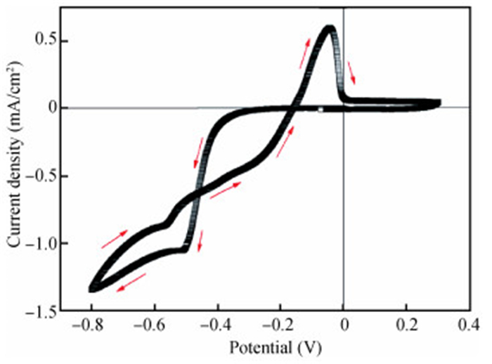
Fig. 1.
The cyclic voltammogram from aqueous solution containing 0.05 M Cu sulfate and 0.05 M C6H8O7 at pH of 6 and scan rate of 20 mV/s.
SEMICONDUCTOR MATERIALS
D. Mohra1, M. Benhaliliba1, , M. Serin2, M.R. Khelladi3, H. Lahmar3 and A. Azizi3
Corresponding author: M. Benhaliliba, Email: mbenhaliliba@gmail.com
Abstract: The thin films of Cu2O are deposited by electrodeposition technique onto indium tin oxide (ITO)-coated glass substrate at different potentials. The precursor is an aqueous solution which contains respectively 0.05 M of CuSO4 and citric acid at kept temperature of 60℃ and the applied potential varies within the {-0.4 V,-0.7 V} SCE range. Based on the chronocoulometry (CC) process, the electrochemical, structural and optical parameters are determined. We measured the current as function of potential within the {-0.4 V,-0.7 V} range and the higher current is found to be within the {-0.7 V,-0.3 V} band. The grain sizes are of 12.12 nm and 35.47 nm according to (110) and (221) orientations respectively. The high textural coefficient of 0.943 is recorded for the potential-0.7 V. The transmittance of 72.25 %, within the visible band, is obtained for the as-grown layer at-0.4 V and the band gap is found to be 2.2 eV for the electrodeposition potential of-0.7 V.
Keywords: Cu2O films, chronocoulometry, electrodeposition, ITO substrate, voltammogram, cathodic potential
| [1] |
Chatterjee S, Sudip K S, Amlan J P. Formation of all-oxide solar cells in atmospheric condition based on Cu2O thin-films grown through SILAR technique. Solar Energy Materials & Solar Cells, 2016, 147: 17
|
| [2] |
Hsueh H T, Chang S J, Hung F Y, et al. Fabrication of coaxial p-Cu2O/n-ZnO nanowire photodiodes. Superlattices and Microstructures, 2011, 49: 572 doi: 10.1016/j.spmi.2011.03.011
|
| [3] |
Wang L C, De Tacconi N R, Chenthamarakshan C R, et al. Electrodeposition copper oxide films: effect of bath pH on grain orientation and orientation-dependant interfacial behavior. Thin Solid Films, 2007, 515: 3090 doi: 10.1016/j.tsf.2006.08.041
|
| [4] |
Pan F, Gao S, Chen C, et al. Recent progress in resistive random access memories: materials, switching mechanisms, and performance. Materials Science and Engineering R, 2004, 83: 1 http://cn.bing.com/academic/profile?id=2034876082&encoded=0&v=paper_preview&mkt=zh-cn
|
| [5] |
Zhang Z, Hu W, Zhong Y C, et al. The effect of complexing agents on the oriented growth of electrodeposited microcrystalline cuprous oxide film. Materials Research Bulletin, 2012, 47: 2561 doi: 10.1016/j.materresbull.2012.04.146
|
| [6] |
Al-Kuhaili M F. Characterization of copper oxide thin films deposited by the thermal evaporation of cuprous oxide (Cu2O). Vacuum, 2008, 82: 623 doi: 10.1016/j.vacuum.2007.10.004
|
| [7] |
Laia G, Wub Y, Linb L, et al. Low resistivity of N-doped Cu2O thin films deposited by RF-magnetron sputtering. Applied Surface Science, 2013, 285: 755 doi: 10.1016/j.apsusc.2013.08.122
|
| [8] |
Kayani Z N, Ali Y, Kiran F, et al. Fabrication of copper oxide nanoparticles by sol-gel route. Materials Today: Proceedings, 2015, 2: 5446 doi: 10.1016/j.matpr.2015.11.067
|
| [9] |
Kasmi A, Yu Tian Z, Vieker H, et al. Innovative CVD synthesis of Cu2O catalysts for CO oxidation. Applied Catalysis B, 2016, 186: 10 doi: 10.1016/j.apcatb.2015.12.034
|
| [10] |
Lva J, Xua J, Zhao M, et al. Effect of seed layer on optical properties and visible photoresponse of ZnO/Cu2O composite thin films. Ceramics International, 2015, 41: 13983 doi: 10.1016/j.ceramint.2015.07.010
|
| [11] |
Yan D, Li S, Hu M, et al. Electrochemical synthesis and the gas sensing properties of the Cu2O nanofilms/porous silicon hybrid structure. Sensors and Actuators B, 2016, 223: 626 doi: 10.1016/j.snb.2015.09.080
|
| [12] |
Khelladi M R, Mentar L, Benaiche A, et al. A study on electrodeposited zinc oxide nanostructures. J Mater Sci: Mater Electron, 2013 24: 153 doi: 10.1007/s10854-012-0973-5
|
| [13] |
Meng H, Yang W, Yan X, et al. A highly sensitive and fast responsive semiconductor metal oxide detector based on In2O3 nanoparticle film for portable gas chromatograph. Sensors and Actuators B, 2015, 216: 511 doi: 10.1016/j.snb.2015.04.068
|
| [14] |
Benhaliliba M, Benouis C E, Yakuphanoglu F, et al. Detailed investigation of submicrometer-sized grains of chemically sprayed (Sn1-xAlx, O2) (0 ≤qslant x ≤qslant 0.085) thin films. Journal of Alloys and Compounds, 2012, 527: 40 doi: 10.1016/j.jallcom.2012.02.128
|
| [15] |
Jiang S, Wu M, Zhou Y, et al. Effects of electrodeposition conditions on the microstructures of ZnO thin films. Integrated Ferroelectrics, 2007, 88: 33 doi: 10.1080/10584580601098563
|
| [16] |
Bard A J, Faulkner L R. Electrochemical methods: fundamentals and applications. Wiley, 2001
|
| [17] |
Wang L, Tao M. Fabrication and characterization of p-n homojunction in cuprous oxide by electrochemical deposition. Electrochem Solid State Lett, 2007, 10: 248 doi: 10.1149/1.2748632
|
| [18] |
Laidoudi S, Bioud A Y, Azizi A, et al. Growth and characterization of electrodeposited Cu2O thin films. Semicond Sci Technol, 2013, 28: 115005 doi: 10.1088/0268-1242/28/11/115005
|
| [19] |
Chatterjee A P, Mukhopadhyay A K, Chakraborty A K, et al. Electrodeposition and characterization of cuprous oxide films. Materials Letters, 1991, 11: 10 doi: 10.1016/0167-577X(91)90180-E
|
| [20] |
Lee Y H, Leu I C, Liao C L, et al. The structural evolution and electrochemical properties of the textured Cu2O thin films. Journal of Alloys and Compounds, 2007, 436: 241 doi: 10.1016/j.jallcom.2006.07.019
|
| [21] |
Hsu Y K , Wu J R, Chen M H, et al. Fabrication of homojunction Cu2O solar cells by electrochemical deposition. Applied Surface Science, 2015, 354: 8 doi: 10.1016/j.apsusc.2015.05.142
|
| [22] |
No Y S, Oh D H, Su K S, et al. Structural, optical, and electrical properties of Cu2O nanocubes grown on indium-tin-oxide-coated glass substrates by using seed-layer-free electrochemical deposition method. Applied Surface Science, 2012, 258: 7581 doi: 10.1016/j.apsusc.2012.04.091
|
| [23] |
Benhaliliba M, Benouis C E, Tiburcio-Silver A. Low copper doped CdO nanowires grown by sol-gel route. Journal of New Technology and Materials, 2011, 1: 24 https://www.researchgate.net/publication/256117103_Low_Copper_Doped_CdO_Nanowires_Grown_by_Sol-Gel_Route
|
| [24] |
Messaoudi O, Makhlouf H, Souissi A, et al. Correlation between optical and structural properties of copper oxide electrodeposited on ITO glass. Journal of Alloys and Compounds, 2014, 611: 142 doi: 10.1016/j.jallcom.2014.05.055
|
| [25] |
Tounsi N, Barhoumi A, Akkari F C, et al. Structural and optical characterization of copper oxide composite thin films elaborated by GLAD technique. Vacuum, 2015, 121: 9 doi: 10.1016/j.vacuum.2015.07.011
|
| [26] |
Kim M S, Kim D Y, Cho M Y, et al. Effects of buffer layer thickness on properties of ZnO thin films grown on porous silicon by plasma-assisted molecular beam epitaxy. Vacuum, 2012, 86: 1373 doi: 10.1016/j.vacuum.2012.01.006
|
| [27] |
Zhang D K, Liu Y C, Liu Y L, et al. The electrical properties and the interfaces of Cu2O/ZnO/ITO p-i-n heterojunction. Physica B, 2004, 351: 178 doi: 10.1016/j.physb.2004.06.003
|
| [28] |
Han K. Electrodeposited cuprous oxide solar cells. The University of Texas At Arlington, December 2009
|
| [29] |
Tombak A, Benhaliliba M, Ocak Y S, et al. The novel transparent sputtered p-type CuO thin films and Ag/p-CuO/n-Si Schottky diode applications. Results in Physics, 2015, 5: 314 doi: 10.1016/j.rinp.2015.11.001
|
| [30] |
Benouis C E, Benhaliliba M, Yakuphanoglu F, et al. Physical properties of ultrasonic sprayed nanosized indium doped SnO2 films. Synthetic Metals, 2011, 161: 1509 doi: 10.1016/j.synthmet.2011.04.017
|
| [31] |
Brandt I S, Martins C A, Zoldan V C, et al. Structural and optical properties of Cu2O crystalline electrodeposited films. Thin Solid Films, 2014, 562: 144 doi: 10.1016/j.tsf.2014.04.013
|
| [32] |
Ravindra N M, Srivastava V K. Variation of refractive index with energy gap in semiconductors. Infrared Phys, 1979, 19: 603 doi: 10.1016/0020-0891(79)90081-2
|
| [33] |
Gupta V P, Ravindra N M. Comments on the moss formula. Phys Stat Sol B, 1980, 100: 715 doi: 10.1002/(ISSN)1521-3951
|
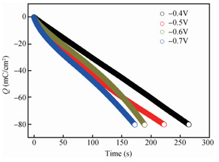
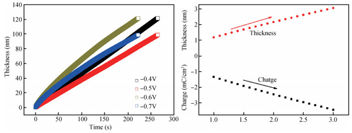
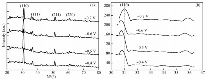
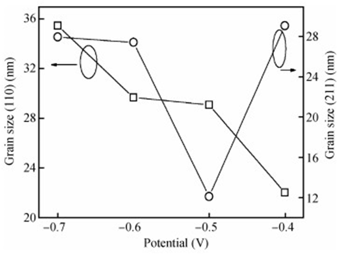
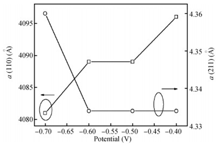
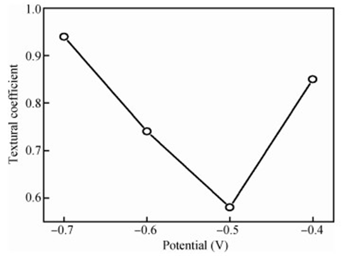
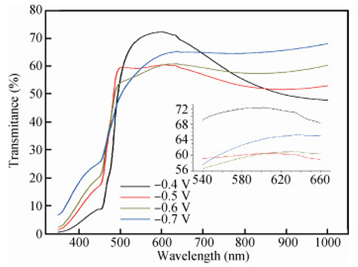
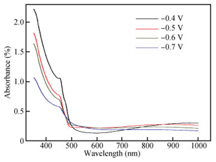
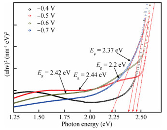
Table 1. The calculated structural parameters of (110) planes of the electrodeposited Cu2O/ITO thin films.

|
Table 2. The calculated structural parameters of (211) planes of the electrodeposited Cu2O/ITO thin films.

|
Table 3. Optical parameters of Cu2O/ITO layers grown at different potentials.

|
| [1] |
Chatterjee S, Sudip K S, Amlan J P. Formation of all-oxide solar cells in atmospheric condition based on Cu2O thin-films grown through SILAR technique. Solar Energy Materials & Solar Cells, 2016, 147: 17
|
| [2] |
Hsueh H T, Chang S J, Hung F Y, et al. Fabrication of coaxial p-Cu2O/n-ZnO nanowire photodiodes. Superlattices and Microstructures, 2011, 49: 572 doi: 10.1016/j.spmi.2011.03.011
|
| [3] |
Wang L C, De Tacconi N R, Chenthamarakshan C R, et al. Electrodeposition copper oxide films: effect of bath pH on grain orientation and orientation-dependant interfacial behavior. Thin Solid Films, 2007, 515: 3090 doi: 10.1016/j.tsf.2006.08.041
|
| [4] |
Pan F, Gao S, Chen C, et al. Recent progress in resistive random access memories: materials, switching mechanisms, and performance. Materials Science and Engineering R, 2004, 83: 1 http://cn.bing.com/academic/profile?id=2034876082&encoded=0&v=paper_preview&mkt=zh-cn
|
| [5] |
Zhang Z, Hu W, Zhong Y C, et al. The effect of complexing agents on the oriented growth of electrodeposited microcrystalline cuprous oxide film. Materials Research Bulletin, 2012, 47: 2561 doi: 10.1016/j.materresbull.2012.04.146
|
| [6] |
Al-Kuhaili M F. Characterization of copper oxide thin films deposited by the thermal evaporation of cuprous oxide (Cu2O). Vacuum, 2008, 82: 623 doi: 10.1016/j.vacuum.2007.10.004
|
| [7] |
Laia G, Wub Y, Linb L, et al. Low resistivity of N-doped Cu2O thin films deposited by RF-magnetron sputtering. Applied Surface Science, 2013, 285: 755 doi: 10.1016/j.apsusc.2013.08.122
|
| [8] |
Kayani Z N, Ali Y, Kiran F, et al. Fabrication of copper oxide nanoparticles by sol-gel route. Materials Today: Proceedings, 2015, 2: 5446 doi: 10.1016/j.matpr.2015.11.067
|
| [9] |
Kasmi A, Yu Tian Z, Vieker H, et al. Innovative CVD synthesis of Cu2O catalysts for CO oxidation. Applied Catalysis B, 2016, 186: 10 doi: 10.1016/j.apcatb.2015.12.034
|
| [10] |
Lva J, Xua J, Zhao M, et al. Effect of seed layer on optical properties and visible photoresponse of ZnO/Cu2O composite thin films. Ceramics International, 2015, 41: 13983 doi: 10.1016/j.ceramint.2015.07.010
|
| [11] |
Yan D, Li S, Hu M, et al. Electrochemical synthesis and the gas sensing properties of the Cu2O nanofilms/porous silicon hybrid structure. Sensors and Actuators B, 2016, 223: 626 doi: 10.1016/j.snb.2015.09.080
|
| [12] |
Khelladi M R, Mentar L, Benaiche A, et al. A study on electrodeposited zinc oxide nanostructures. J Mater Sci: Mater Electron, 2013 24: 153 doi: 10.1007/s10854-012-0973-5
|
| [13] |
Meng H, Yang W, Yan X, et al. A highly sensitive and fast responsive semiconductor metal oxide detector based on In2O3 nanoparticle film for portable gas chromatograph. Sensors and Actuators B, 2015, 216: 511 doi: 10.1016/j.snb.2015.04.068
|
| [14] |
Benhaliliba M, Benouis C E, Yakuphanoglu F, et al. Detailed investigation of submicrometer-sized grains of chemically sprayed (Sn1-xAlx, O2) (0 ≤qslant x ≤qslant 0.085) thin films. Journal of Alloys and Compounds, 2012, 527: 40 doi: 10.1016/j.jallcom.2012.02.128
|
| [15] |
Jiang S, Wu M, Zhou Y, et al. Effects of electrodeposition conditions on the microstructures of ZnO thin films. Integrated Ferroelectrics, 2007, 88: 33 doi: 10.1080/10584580601098563
|
| [16] |
Bard A J, Faulkner L R. Electrochemical methods: fundamentals and applications. Wiley, 2001
|
| [17] |
Wang L, Tao M. Fabrication and characterization of p-n homojunction in cuprous oxide by electrochemical deposition. Electrochem Solid State Lett, 2007, 10: 248 doi: 10.1149/1.2748632
|
| [18] |
Laidoudi S, Bioud A Y, Azizi A, et al. Growth and characterization of electrodeposited Cu2O thin films. Semicond Sci Technol, 2013, 28: 115005 doi: 10.1088/0268-1242/28/11/115005
|
| [19] |
Chatterjee A P, Mukhopadhyay A K, Chakraborty A K, et al. Electrodeposition and characterization of cuprous oxide films. Materials Letters, 1991, 11: 10 doi: 10.1016/0167-577X(91)90180-E
|
| [20] |
Lee Y H, Leu I C, Liao C L, et al. The structural evolution and electrochemical properties of the textured Cu2O thin films. Journal of Alloys and Compounds, 2007, 436: 241 doi: 10.1016/j.jallcom.2006.07.019
|
| [21] |
Hsu Y K , Wu J R, Chen M H, et al. Fabrication of homojunction Cu2O solar cells by electrochemical deposition. Applied Surface Science, 2015, 354: 8 doi: 10.1016/j.apsusc.2015.05.142
|
| [22] |
No Y S, Oh D H, Su K S, et al. Structural, optical, and electrical properties of Cu2O nanocubes grown on indium-tin-oxide-coated glass substrates by using seed-layer-free electrochemical deposition method. Applied Surface Science, 2012, 258: 7581 doi: 10.1016/j.apsusc.2012.04.091
|
| [23] |
Benhaliliba M, Benouis C E, Tiburcio-Silver A. Low copper doped CdO nanowires grown by sol-gel route. Journal of New Technology and Materials, 2011, 1: 24 https://www.researchgate.net/publication/256117103_Low_Copper_Doped_CdO_Nanowires_Grown_by_Sol-Gel_Route
|
| [24] |
Messaoudi O, Makhlouf H, Souissi A, et al. Correlation between optical and structural properties of copper oxide electrodeposited on ITO glass. Journal of Alloys and Compounds, 2014, 611: 142 doi: 10.1016/j.jallcom.2014.05.055
|
| [25] |
Tounsi N, Barhoumi A, Akkari F C, et al. Structural and optical characterization of copper oxide composite thin films elaborated by GLAD technique. Vacuum, 2015, 121: 9 doi: 10.1016/j.vacuum.2015.07.011
|
| [26] |
Kim M S, Kim D Y, Cho M Y, et al. Effects of buffer layer thickness on properties of ZnO thin films grown on porous silicon by plasma-assisted molecular beam epitaxy. Vacuum, 2012, 86: 1373 doi: 10.1016/j.vacuum.2012.01.006
|
| [27] |
Zhang D K, Liu Y C, Liu Y L, et al. The electrical properties and the interfaces of Cu2O/ZnO/ITO p-i-n heterojunction. Physica B, 2004, 351: 178 doi: 10.1016/j.physb.2004.06.003
|
| [28] |
Han K. Electrodeposited cuprous oxide solar cells. The University of Texas At Arlington, December 2009
|
| [29] |
Tombak A, Benhaliliba M, Ocak Y S, et al. The novel transparent sputtered p-type CuO thin films and Ag/p-CuO/n-Si Schottky diode applications. Results in Physics, 2015, 5: 314 doi: 10.1016/j.rinp.2015.11.001
|
| [30] |
Benouis C E, Benhaliliba M, Yakuphanoglu F, et al. Physical properties of ultrasonic sprayed nanosized indium doped SnO2 films. Synthetic Metals, 2011, 161: 1509 doi: 10.1016/j.synthmet.2011.04.017
|
| [31] |
Brandt I S, Martins C A, Zoldan V C, et al. Structural and optical properties of Cu2O crystalline electrodeposited films. Thin Solid Films, 2014, 562: 144 doi: 10.1016/j.tsf.2014.04.013
|
| [32] |
Ravindra N M, Srivastava V K. Variation of refractive index with energy gap in semiconductors. Infrared Phys, 1979, 19: 603 doi: 10.1016/0020-0891(79)90081-2
|
| [33] |
Gupta V P, Ravindra N M. Comments on the moss formula. Phys Stat Sol B, 1980, 100: 715 doi: 10.1002/(ISSN)1521-3951
|


Article views: 3913 Times PDF downloads: 54 Times Cited by: 0 Times
Received: 17 February 2016 Revised: 18 May 2016 Online: Published: 01 October 2016
| Citation: |
D. Mohra, M. Benhaliliba, M. Serin, M.R. Khelladi, H. Lahmar, A. Azizi. The investigation of electrodeposited Cu2O/ITO layers by chronocoulometry process: effect of electrical potential[J]. Journal of Semiconductors, 2016, 37(10): 103001. doi: 10.1088/1674-4926/37/10/103001
****
D. Mohra, M. Benhaliliba, M. Serin, M.R. Khelladi, H. Lahmar, A. Azizi. The investigation of electrodeposited Cu2O/ITO layers by chronocoulometry process: effect of electrical potential[J]. J. Semicond., 2016, 37(10): 103001. doi: 10.1088/1674-4926/37/10/103001.

|
| [1] |
Chatterjee S, Sudip K S, Amlan J P. Formation of all-oxide solar cells in atmospheric condition based on Cu2O thin-films grown through SILAR technique. Solar Energy Materials & Solar Cells, 2016, 147: 17
|
| [2] |
Hsueh H T, Chang S J, Hung F Y, et al. Fabrication of coaxial p-Cu2O/n-ZnO nanowire photodiodes. Superlattices and Microstructures, 2011, 49: 572 doi: 10.1016/j.spmi.2011.03.011
|
| [3] |
Wang L C, De Tacconi N R, Chenthamarakshan C R, et al. Electrodeposition copper oxide films: effect of bath pH on grain orientation and orientation-dependant interfacial behavior. Thin Solid Films, 2007, 515: 3090 doi: 10.1016/j.tsf.2006.08.041
|
| [4] |
Pan F, Gao S, Chen C, et al. Recent progress in resistive random access memories: materials, switching mechanisms, and performance. Materials Science and Engineering R, 2004, 83: 1 http://cn.bing.com/academic/profile?id=2034876082&encoded=0&v=paper_preview&mkt=zh-cn
|
| [5] |
Zhang Z, Hu W, Zhong Y C, et al. The effect of complexing agents on the oriented growth of electrodeposited microcrystalline cuprous oxide film. Materials Research Bulletin, 2012, 47: 2561 doi: 10.1016/j.materresbull.2012.04.146
|
| [6] |
Al-Kuhaili M F. Characterization of copper oxide thin films deposited by the thermal evaporation of cuprous oxide (Cu2O). Vacuum, 2008, 82: 623 doi: 10.1016/j.vacuum.2007.10.004
|
| [7] |
Laia G, Wub Y, Linb L, et al. Low resistivity of N-doped Cu2O thin films deposited by RF-magnetron sputtering. Applied Surface Science, 2013, 285: 755 doi: 10.1016/j.apsusc.2013.08.122
|
| [8] |
Kayani Z N, Ali Y, Kiran F, et al. Fabrication of copper oxide nanoparticles by sol-gel route. Materials Today: Proceedings, 2015, 2: 5446 doi: 10.1016/j.matpr.2015.11.067
|
| [9] |
Kasmi A, Yu Tian Z, Vieker H, et al. Innovative CVD synthesis of Cu2O catalysts for CO oxidation. Applied Catalysis B, 2016, 186: 10 doi: 10.1016/j.apcatb.2015.12.034
|
| [10] |
Lva J, Xua J, Zhao M, et al. Effect of seed layer on optical properties and visible photoresponse of ZnO/Cu2O composite thin films. Ceramics International, 2015, 41: 13983 doi: 10.1016/j.ceramint.2015.07.010
|
| [11] |
Yan D, Li S, Hu M, et al. Electrochemical synthesis and the gas sensing properties of the Cu2O nanofilms/porous silicon hybrid structure. Sensors and Actuators B, 2016, 223: 626 doi: 10.1016/j.snb.2015.09.080
|
| [12] |
Khelladi M R, Mentar L, Benaiche A, et al. A study on electrodeposited zinc oxide nanostructures. J Mater Sci: Mater Electron, 2013 24: 153 doi: 10.1007/s10854-012-0973-5
|
| [13] |
Meng H, Yang W, Yan X, et al. A highly sensitive and fast responsive semiconductor metal oxide detector based on In2O3 nanoparticle film for portable gas chromatograph. Sensors and Actuators B, 2015, 216: 511 doi: 10.1016/j.snb.2015.04.068
|
| [14] |
Benhaliliba M, Benouis C E, Yakuphanoglu F, et al. Detailed investigation of submicrometer-sized grains of chemically sprayed (Sn1-xAlx, O2) (0 ≤qslant x ≤qslant 0.085) thin films. Journal of Alloys and Compounds, 2012, 527: 40 doi: 10.1016/j.jallcom.2012.02.128
|
| [15] |
Jiang S, Wu M, Zhou Y, et al. Effects of electrodeposition conditions on the microstructures of ZnO thin films. Integrated Ferroelectrics, 2007, 88: 33 doi: 10.1080/10584580601098563
|
| [16] |
Bard A J, Faulkner L R. Electrochemical methods: fundamentals and applications. Wiley, 2001
|
| [17] |
Wang L, Tao M. Fabrication and characterization of p-n homojunction in cuprous oxide by electrochemical deposition. Electrochem Solid State Lett, 2007, 10: 248 doi: 10.1149/1.2748632
|
| [18] |
Laidoudi S, Bioud A Y, Azizi A, et al. Growth and characterization of electrodeposited Cu2O thin films. Semicond Sci Technol, 2013, 28: 115005 doi: 10.1088/0268-1242/28/11/115005
|
| [19] |
Chatterjee A P, Mukhopadhyay A K, Chakraborty A K, et al. Electrodeposition and characterization of cuprous oxide films. Materials Letters, 1991, 11: 10 doi: 10.1016/0167-577X(91)90180-E
|
| [20] |
Lee Y H, Leu I C, Liao C L, et al. The structural evolution and electrochemical properties of the textured Cu2O thin films. Journal of Alloys and Compounds, 2007, 436: 241 doi: 10.1016/j.jallcom.2006.07.019
|
| [21] |
Hsu Y K , Wu J R, Chen M H, et al. Fabrication of homojunction Cu2O solar cells by electrochemical deposition. Applied Surface Science, 2015, 354: 8 doi: 10.1016/j.apsusc.2015.05.142
|
| [22] |
No Y S, Oh D H, Su K S, et al. Structural, optical, and electrical properties of Cu2O nanocubes grown on indium-tin-oxide-coated glass substrates by using seed-layer-free electrochemical deposition method. Applied Surface Science, 2012, 258: 7581 doi: 10.1016/j.apsusc.2012.04.091
|
| [23] |
Benhaliliba M, Benouis C E, Tiburcio-Silver A. Low copper doped CdO nanowires grown by sol-gel route. Journal of New Technology and Materials, 2011, 1: 24 https://www.researchgate.net/publication/256117103_Low_Copper_Doped_CdO_Nanowires_Grown_by_Sol-Gel_Route
|
| [24] |
Messaoudi O, Makhlouf H, Souissi A, et al. Correlation between optical and structural properties of copper oxide electrodeposited on ITO glass. Journal of Alloys and Compounds, 2014, 611: 142 doi: 10.1016/j.jallcom.2014.05.055
|
| [25] |
Tounsi N, Barhoumi A, Akkari F C, et al. Structural and optical characterization of copper oxide composite thin films elaborated by GLAD technique. Vacuum, 2015, 121: 9 doi: 10.1016/j.vacuum.2015.07.011
|
| [26] |
Kim M S, Kim D Y, Cho M Y, et al. Effects of buffer layer thickness on properties of ZnO thin films grown on porous silicon by plasma-assisted molecular beam epitaxy. Vacuum, 2012, 86: 1373 doi: 10.1016/j.vacuum.2012.01.006
|
| [27] |
Zhang D K, Liu Y C, Liu Y L, et al. The electrical properties and the interfaces of Cu2O/ZnO/ITO p-i-n heterojunction. Physica B, 2004, 351: 178 doi: 10.1016/j.physb.2004.06.003
|
| [28] |
Han K. Electrodeposited cuprous oxide solar cells. The University of Texas At Arlington, December 2009
|
| [29] |
Tombak A, Benhaliliba M, Ocak Y S, et al. The novel transparent sputtered p-type CuO thin films and Ag/p-CuO/n-Si Schottky diode applications. Results in Physics, 2015, 5: 314 doi: 10.1016/j.rinp.2015.11.001
|
| [30] |
Benouis C E, Benhaliliba M, Yakuphanoglu F, et al. Physical properties of ultrasonic sprayed nanosized indium doped SnO2 films. Synthetic Metals, 2011, 161: 1509 doi: 10.1016/j.synthmet.2011.04.017
|
| [31] |
Brandt I S, Martins C A, Zoldan V C, et al. Structural and optical properties of Cu2O crystalline electrodeposited films. Thin Solid Films, 2014, 562: 144 doi: 10.1016/j.tsf.2014.04.013
|
| [32] |
Ravindra N M, Srivastava V K. Variation of refractive index with energy gap in semiconductors. Infrared Phys, 1979, 19: 603 doi: 10.1016/0020-0891(79)90081-2
|
| [33] |
Gupta V P, Ravindra N M. Comments on the moss formula. Phys Stat Sol B, 1980, 100: 715 doi: 10.1002/(ISSN)1521-3951
|

 WeChat ID
Journal of Semiconductors © 2017 All Rights Reserved 京ICP备05085259号-2

 DownLoad:

