


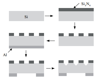
Fig. 1.
Prestructuring process for both sides of the silicon wafer.
SEMICONDUCTOR TECHNOLOGY
Yaohu Lei, Zhigang Zhao, Jinchuan Guo, Ji Li and Hanben Niu
Corresponding author: Li Ji, Email: liji@szu.edu.cn; Niu Hanben, Email: hbniu@szu.edu.cn
Abstract: The fabrication of ordered, high aspect-ratio microstructures in silicon by use of photo-assisted electrochemical etching is an important technology, where voltage and current density are significant factors. In this paper, disordered walls appear in 5-inch n-type silicon wafers when a large current density is used. Based on the theory of space charge region, these disordered walls are caused by the contradiction between the protection from dissolution by a high applied voltage and the dissolution by a high current density. To verify this point, wall arrays were fabricated at different applied voltages and current densities. Moreover, the critical voltage was kept constant and different current densities were applied to obtain conditions for avoiding disordered walls and achieving uniform wall arrays. Finally, a wall array with a period of 5.6μm and a depth of 55μm was achieved at an applied voltage of 3 V and a monotonically increasing current density ranging from 22.9 to 24.5 mA/cm2.
Keywords: electrochemical etching, wall array, high aspect-ratio, silicon, disordered wall
| [1] |
González E Q, Wusu E O, Carstensen J, et al. How to make optimized arrays of Si wires suitable as superior anode for Li-ion batteries. J Electrochem Soc, 2011, 158(11): E119 doi: 10.1149/2.069111jes
|
| [2] |
Lei Y H, Liu X, Guo J C, et al. Development of X-ray scintillator functioning also as an analyser grating used in grating-based X-ray differential phase contrast imaging. Chin Phys B, 2011, 20(4): 042901 doi: 10.1088/1674-1056/20/4/042901
|
| [3] |
Chen X, Lin J, Yuan D, et al. Obtaining of high area-ratio free standing silicon microchannel plate via modified electrochemical procedure. J Micromech Microeng, 2008, 18(3): 037003 doi: 10.1088/0960-1317/18/3/037003
|
| [4] |
Kraeh C, Popsecu A, Schieber M, et al. Fabrication of high aspect ratio microtube arrays for 2D photonic crystals. Mater Res Express, 2014, 1: 026201 doi: 10.1088/2053-1591/1/2/026201
|
| [5] |
Peng Bobo, Wang Fei, Liu Tao, et al. Novel method of separating macroporous arrays from p-type silicon substrate. Journal of Semiconductors, 2012, 33(4): 043004 doi: 10.1088/1674-4926/33/4/043004
|
| [6] |
Ottow S, Lehmann V, Föll H. Development of three-dimensional microstructure processing using macroporous n-type silicon. Appl Phys A, 1996, 63:153 http://www.researchgate.net/publication/225670039_Development_of_three-dimensional_microstructure_processing_using_macroporous_n-type_silicon
|
| [7] |
Bassu M, Surdo S, Strambini L M, et al. Electrochemical micromachining as an enabling technology for advanced silicon microstructure. Adv Funct Mater, 2012, 22: 1222 doi: 10.1002/adfm.v22.6
|
| [8] |
Astrova E V, Fedulova G V. Formation of deep periodic trenches in photo-electrochemical etching of n-type silicon. J Micromech Microeng, 2009, 19: 095009 doi: 10.1088/0960-1317/19/9/095009
|
| [9] |
Lei Y H, Guo J C, Zhao Z G, et al. Study of deep etching in silicon by photo-assisted electrochemical technique. Semiconductor Technology, 2010, 35(6): 517 (in Chinese)
|
| [10] |
Lehmann V. The physics of macropore formation in low doped n-type silicon. J Electrochem Soc, 1993, 140(10): 2836 doi: 10.1149/1.2220919
|
| [11] |
Wang G, Fu S, Chen L, et al. Influence of voltage on photo-electrochemical etching of n-type macroporous silicon arrays. Journal of Semiconductors, 2010, 31(11): 116002 doi: 10.1088/1674-4926/31/11/116002
|
| [12] |
Wang G, Chen L, Qin X, et al. Influence of etching current density on the morphology of macroporous silicon arrays by photo-electrochemical etching. Journal of Semiconductors, 2010, 31(7): 074011 doi: 10.1088/1674-4926/31/7/074011
|
| [13] |
Lin J C, Lai C M, Jehng W D, et al. Effect of ethanol on the photoelectrochemical fabrication of macroporous n-Si (100) in HF solution. J Electrochem Soc, 2008, 155(6): D436 doi: 10.1149/1.2898687
|
| [14] |
Zhao Z, Guo J, Lei Y, et al. Photoelectrochemical etching of uniform macropore array on full 5-inch silicon wafers. Journal of Semiconductors, 2010, 31(7): 076001 doi: 10.1088/1674-4926/31/7/076001
|
| [15] |
Zhang X G. Mechanism of pore formation on n-type silicon. J Electrochem Soc, 1991, 138(12): 3750 doi: 10.1149/1.2085494
|
| [16] |
Föll H, Christophersen M, Carstensen J, et al. Formation and application of porous silicon. Mater Sci Eng R, 2002, 39: 93 doi: 10.1016/S0927-796X(02)00090-6
|
| [17] |
Geppert T, Schweizer S L, Gösele U, et al. Deep trench etching in macroporous silicon. Appl Phys A, 2006, 84: 237 doi: 10.1007/s00339-006-3628-7
|
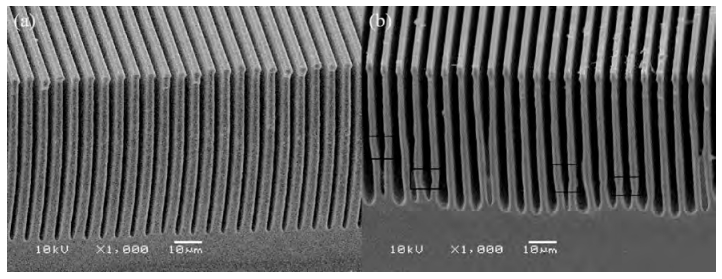
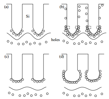
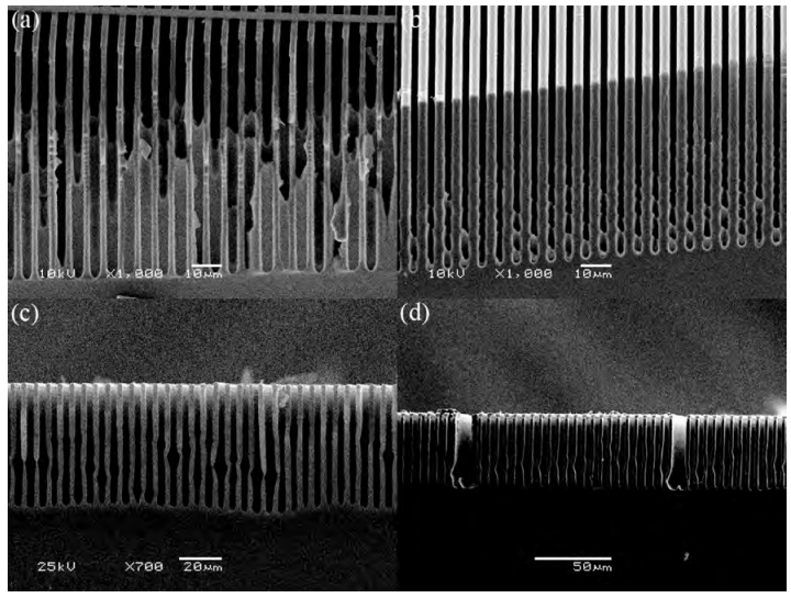
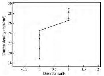
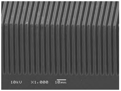
Table 1. Etching conditions and results.

|
| [1] |
González E Q, Wusu E O, Carstensen J, et al. How to make optimized arrays of Si wires suitable as superior anode for Li-ion batteries. J Electrochem Soc, 2011, 158(11): E119 doi: 10.1149/2.069111jes
|
| [2] |
Lei Y H, Liu X, Guo J C, et al. Development of X-ray scintillator functioning also as an analyser grating used in grating-based X-ray differential phase contrast imaging. Chin Phys B, 2011, 20(4): 042901 doi: 10.1088/1674-1056/20/4/042901
|
| [3] |
Chen X, Lin J, Yuan D, et al. Obtaining of high area-ratio free standing silicon microchannel plate via modified electrochemical procedure. J Micromech Microeng, 2008, 18(3): 037003 doi: 10.1088/0960-1317/18/3/037003
|
| [4] |
Kraeh C, Popsecu A, Schieber M, et al. Fabrication of high aspect ratio microtube arrays for 2D photonic crystals. Mater Res Express, 2014, 1: 026201 doi: 10.1088/2053-1591/1/2/026201
|
| [5] |
Peng Bobo, Wang Fei, Liu Tao, et al. Novel method of separating macroporous arrays from p-type silicon substrate. Journal of Semiconductors, 2012, 33(4): 043004 doi: 10.1088/1674-4926/33/4/043004
|
| [6] |
Ottow S, Lehmann V, Föll H. Development of three-dimensional microstructure processing using macroporous n-type silicon. Appl Phys A, 1996, 63:153 http://www.researchgate.net/publication/225670039_Development_of_three-dimensional_microstructure_processing_using_macroporous_n-type_silicon
|
| [7] |
Bassu M, Surdo S, Strambini L M, et al. Electrochemical micromachining as an enabling technology for advanced silicon microstructure. Adv Funct Mater, 2012, 22: 1222 doi: 10.1002/adfm.v22.6
|
| [8] |
Astrova E V, Fedulova G V. Formation of deep periodic trenches in photo-electrochemical etching of n-type silicon. J Micromech Microeng, 2009, 19: 095009 doi: 10.1088/0960-1317/19/9/095009
|
| [9] |
Lei Y H, Guo J C, Zhao Z G, et al. Study of deep etching in silicon by photo-assisted electrochemical technique. Semiconductor Technology, 2010, 35(6): 517 (in Chinese)
|
| [10] |
Lehmann V. The physics of macropore formation in low doped n-type silicon. J Electrochem Soc, 1993, 140(10): 2836 doi: 10.1149/1.2220919
|
| [11] |
Wang G, Fu S, Chen L, et al. Influence of voltage on photo-electrochemical etching of n-type macroporous silicon arrays. Journal of Semiconductors, 2010, 31(11): 116002 doi: 10.1088/1674-4926/31/11/116002
|
| [12] |
Wang G, Chen L, Qin X, et al. Influence of etching current density on the morphology of macroporous silicon arrays by photo-electrochemical etching. Journal of Semiconductors, 2010, 31(7): 074011 doi: 10.1088/1674-4926/31/7/074011
|
| [13] |
Lin J C, Lai C M, Jehng W D, et al. Effect of ethanol on the photoelectrochemical fabrication of macroporous n-Si (100) in HF solution. J Electrochem Soc, 2008, 155(6): D436 doi: 10.1149/1.2898687
|
| [14] |
Zhao Z, Guo J, Lei Y, et al. Photoelectrochemical etching of uniform macropore array on full 5-inch silicon wafers. Journal of Semiconductors, 2010, 31(7): 076001 doi: 10.1088/1674-4926/31/7/076001
|
| [15] |
Zhang X G. Mechanism of pore formation on n-type silicon. J Electrochem Soc, 1991, 138(12): 3750 doi: 10.1149/1.2085494
|
| [16] |
Föll H, Christophersen M, Carstensen J, et al. Formation and application of porous silicon. Mater Sci Eng R, 2002, 39: 93 doi: 10.1016/S0927-796X(02)00090-6
|
| [17] |
Geppert T, Schweizer S L, Gösele U, et al. Deep trench etching in macroporous silicon. Appl Phys A, 2006, 84: 237 doi: 10.1007/s00339-006-3628-7
|


Article views: 3731 Times PDF downloads: 22 Times Cited by: 0 Times
Received: 21 December 2015 Revised: 03 March 2016 Online: Published: 01 October 2016
| Citation: |
Yaohu Lei, Zhigang Zhao, Jinchuan Guo, Ji Li, Hanben Niu. Disordered wall arrays by photo-assisted electrochemical etching in n-type silicon[J]. Journal of Semiconductors, 2016, 37(10): 106001. doi: 10.1088/1674-4926/37/10/106001
****
Y H Lei, Z G Zhao, J C Guo, J Li, H B Niu. Disordered wall arrays by photo-assisted electrochemical etching in n-type silicon[J]. J. Semicond., 2016, 37(10): 106001. doi: 10.1088/1674-4926/37/10/106001.

|
| [1] |
González E Q, Wusu E O, Carstensen J, et al. How to make optimized arrays of Si wires suitable as superior anode for Li-ion batteries. J Electrochem Soc, 2011, 158(11): E119 doi: 10.1149/2.069111jes
|
| [2] |
Lei Y H, Liu X, Guo J C, et al. Development of X-ray scintillator functioning also as an analyser grating used in grating-based X-ray differential phase contrast imaging. Chin Phys B, 2011, 20(4): 042901 doi: 10.1088/1674-1056/20/4/042901
|
| [3] |
Chen X, Lin J, Yuan D, et al. Obtaining of high area-ratio free standing silicon microchannel plate via modified electrochemical procedure. J Micromech Microeng, 2008, 18(3): 037003 doi: 10.1088/0960-1317/18/3/037003
|
| [4] |
Kraeh C, Popsecu A, Schieber M, et al. Fabrication of high aspect ratio microtube arrays for 2D photonic crystals. Mater Res Express, 2014, 1: 026201 doi: 10.1088/2053-1591/1/2/026201
|
| [5] |
Peng Bobo, Wang Fei, Liu Tao, et al. Novel method of separating macroporous arrays from p-type silicon substrate. Journal of Semiconductors, 2012, 33(4): 043004 doi: 10.1088/1674-4926/33/4/043004
|
| [6] |
Ottow S, Lehmann V, Föll H. Development of three-dimensional microstructure processing using macroporous n-type silicon. Appl Phys A, 1996, 63:153 http://www.researchgate.net/publication/225670039_Development_of_three-dimensional_microstructure_processing_using_macroporous_n-type_silicon
|
| [7] |
Bassu M, Surdo S, Strambini L M, et al. Electrochemical micromachining as an enabling technology for advanced silicon microstructure. Adv Funct Mater, 2012, 22: 1222 doi: 10.1002/adfm.v22.6
|
| [8] |
Astrova E V, Fedulova G V. Formation of deep periodic trenches in photo-electrochemical etching of n-type silicon. J Micromech Microeng, 2009, 19: 095009 doi: 10.1088/0960-1317/19/9/095009
|
| [9] |
Lei Y H, Guo J C, Zhao Z G, et al. Study of deep etching in silicon by photo-assisted electrochemical technique. Semiconductor Technology, 2010, 35(6): 517 (in Chinese)
|
| [10] |
Lehmann V. The physics of macropore formation in low doped n-type silicon. J Electrochem Soc, 1993, 140(10): 2836 doi: 10.1149/1.2220919
|
| [11] |
Wang G, Fu S, Chen L, et al. Influence of voltage on photo-electrochemical etching of n-type macroporous silicon arrays. Journal of Semiconductors, 2010, 31(11): 116002 doi: 10.1088/1674-4926/31/11/116002
|
| [12] |
Wang G, Chen L, Qin X, et al. Influence of etching current density on the morphology of macroporous silicon arrays by photo-electrochemical etching. Journal of Semiconductors, 2010, 31(7): 074011 doi: 10.1088/1674-4926/31/7/074011
|
| [13] |
Lin J C, Lai C M, Jehng W D, et al. Effect of ethanol on the photoelectrochemical fabrication of macroporous n-Si (100) in HF solution. J Electrochem Soc, 2008, 155(6): D436 doi: 10.1149/1.2898687
|
| [14] |
Zhao Z, Guo J, Lei Y, et al. Photoelectrochemical etching of uniform macropore array on full 5-inch silicon wafers. Journal of Semiconductors, 2010, 31(7): 076001 doi: 10.1088/1674-4926/31/7/076001
|
| [15] |
Zhang X G. Mechanism of pore formation on n-type silicon. J Electrochem Soc, 1991, 138(12): 3750 doi: 10.1149/1.2085494
|
| [16] |
Föll H, Christophersen M, Carstensen J, et al. Formation and application of porous silicon. Mater Sci Eng R, 2002, 39: 93 doi: 10.1016/S0927-796X(02)00090-6
|
| [17] |
Geppert T, Schweizer S L, Gösele U, et al. Deep trench etching in macroporous silicon. Appl Phys A, 2006, 84: 237 doi: 10.1007/s00339-006-3628-7
|

 WeChat ID
Journal of Semiconductors © 2017 All Rights Reserved 京ICP备05085259号-2

 DownLoad:

