Processing math: 100%
J. Semicond. > 2016, Volume 37 > Issue 11 > 114004

SEMICONDUCTOR DEVICES

Monolayer-molybdenum-disulfide-based nano-optomechanical transistor andewline tunable nonlinear responses

Huajun Chen, Changzhao Chen, Yang Li and Xianwen Fang

+ Author Affiliations

 Corresponding author: Chen Huajun,chenphysics@126.com

DOI: 10.1088/1674-4926/37/11/114004

PDF

Abstract: Atomically thin two-dimensional semiconductor nanomaterials have attained considerable attention currently. Here, we present a nano-optomechanical system based on a suspended monolayer molybdenum disulfide (MoS2). The linear and nonlinear coherent optical properties of this system, and the phenomenon of phonon-induced transparency are demonstrated. The transmission of the probe field can be manipulated by the power of a second ‘gating' (pump) field, which indicates a promising candidate for an optical transistor. We further study the nonlinear effect of the system, and the optical Kerr effect of the monolayer MoS2 resonator can be regulated under different parameter regimes. This scheme proposed here may indicate potential chip-scale applications of monolayer MoS2 resonator in quantum information with the currently popular pump-probe technology.

Key words: MoS2nanomechanical resonatoroptical transistornonlinear optical effect

Atomically thin two-dimensional (2D) layered materials,such as graphene and monolayer molybdenum disulfide (MoS2),have attracted great interest recently due to their superior electrical-optical properties and potential applications[1-3]. The pristine graphene is a zero-bandgap nanomaterial and several applications requiring a bandgap will be limited. Compared with graphene being a semi-metal,MoS2 is a semiconductor with a thickness-dependent electronic structure[4,5]. With the decrease of the layer numbers of MoS2,the material undergoes a transition from an indirect bandgap (1.2 eV in bulk) to a direct bandgap semiconductor (1.8 eV in monolayer)[6]. Monolayer MoS2 may replace graphene to realize the applications in photodetection[7,8],photovoltaics[9],and MoS2-based transistors[10,11] due to this intrinsic property. In addition,the applications in sensors will benefit from another property of the large surface-to-volume ratio of monolayer MoS2,and chemical sensors based on multilayer and monolayer MoS2 have been demonstrated experimentally[12-14].

As atomically thin 2D layered nanomaterials,graphene and monolayer MoS2 could be considered as the ultimate nanomaterials to structure micromechanical resonators,and additionally,nano-optomechanical systems based on graphene have been obtained experimentally recently[15,16]. For MoS2,multilayer MoS2 nanomechanical resonator[17,18] and single layer MoS2 mechanical resonator[19] have also been realized experimentally,due to its properties of ultralow weight[17],exceptional strain limit[5],and high elastic modulus[20,21]. It is noticed that the applications such as transistors,sensors and nanomechanical systems based on monolayer/multilayer MoS2 mostly focused on the electronic regimes. However,MoS2-based devices and applications in the all-optical domain have not been undertaken yet.

Here,we present a nano-optomechanical system based on a plate-like circular monolayer MoS2 suspended on the Si/SiO2 substrate[17,19]. We investigate the probe absorption and dispersion spectra of the probe field induced by the coupling between the mechanical vibration and the exciton in the monolayer MoS2 resonator,and the phenomenon of phonon-induced transparency (PIT) is also demonstrated due to the exciton-resonator coupling. The transmission of the probe field can be manipulated by the optical pump power,and the probe field can be efficiently attenuated or amplified depending on the power of a second `gating' (pump) field,which indicates a promising candidate for a quantum optical transistor. The exciton-resonator coupling makes a great contribution to this coupled system which induces the significantly enhanced optical nonlinear effect. The optical Kerr effect and nonlinear absorption can be modulated via controlling the intensity of the pump laser. Parameters such as the quality factor of the resonator Q and the exciton-resonator coupling β affecting the optical Kerr effect are also studied.

Figure 1(a) gives the model based on monolayer MoS2[17,19] with the optical pump-probe technology. Figure 1(b) shows the structure of monolayer MoS2 consisting of a hexagonal plane of Mo atoms covalently bonded and sandwiched between two planes of S atoms. Both experiments[22,23] and theories[24,25] have studied the vibrational properties of bulk,few layer,and monolayer MoS2 recently,Although structural nonidealities and asymmetries of devices based on MoS2 nanostructures will occur and cause new mechanical resonances[26],for the sake of analytical simplicity we still take into account the model system as shown in Figure 1[17,19]. In this suspended structure,the lowest-energy resonance corresponds to the fundamental flexural mode and the resonator is assumed to be characterized by sufficiently high quality factor Q. Therefore the lifetime of the resonator is long enough. In this case,the new mechanical resonances caused by the edge effects and irregular shapes should be ignored compared to the fundamental flexural mode.

Figure  1.  (Color online) (a) The proposed setup of monolayer MoS2-based nanomechanical resonator suspended on the Si/SiO2 substrate with the optical pump-probe technique. (b) Molecular structure of MoS2. (c) The energy-level diagram of exciton in the MoS2 coupled to the resonator.

In the system,the lowest-energy resonance corresponds to the fundamental flexural mode,the resonator is assumed to be characterized by sufficiently high quality factor Q,and the lifetime of the resonator is long enough. The new mechanical resonances induced by the edge effects and irregular shapes can be ignored compared to the fundamental flexural mode. For vibrations of suspended MoS2 diaphragms,the fundamental mode resonance frequency can be derived as[27,28] ωm=(kd2)16Dρvd4[(kd2)2+γd44D] ,where D=Ert3/[12(1v2)] is the flexural rigidity with elastic modulus Er,monolayer thickness t,and Poisson ratio v. γ is the tension and ρv is the body mass density. The mode dependent parameter k accompanying the diameter d of the circular diaphragm has the form of , kd/2=α+(βα)eηeρlnx ,where x=γd2/4D . The parameters used are α=14.682,β =21.26,η =0.6613,and ρ =0.5273 refer to Reference [27]. The parameters[17, 19] of the monolayer MoS2 resonator are: the elastic modulus E r =0.2 TPa,monolayer thickness t=0.65 nm,the diameter of the circular diaphragm d=1 μm,the strain ε3 ,the moderate tension γ =4.2 N/m,the Poisson ratio v=0.165,and the body mass density ρv =5.06 g/cm3. Therefore the fundamental vibration frequency of monolayer MoS2 resonator is ωm1.2 GHz.

We introduce the bosonic annihilation (creation) operator a(a)+ to describe the eigenmode of the quantum harmonic oscillator,and HNR = ωm(a+a+1/2) is the Hamiltonian of the monolayer MoS2 resonator. A two-level system with ground state| g > and the first excited state (single exciton) |e > characterized by the pseudospin -1/2 operators S± and Sz can be employed to describe the exciton since the monolayer MoS2 is a direct bandgap semiconductor,and the energy level is shown in Figure 1(c). The Hamiltonian of the localized two-level exciton can be written as He=ωeSz with the exciton frequency ωe . The deformation potential interactions[29]induce the coupling between the exciton in monolayer MoS2 resonator and the flexural motion,and therefore the interaction Hamiltonian between the resonator and the two-level exciton is HNR-e=ωmβSz(a++a) ,where β is the coupling strength.

The pump-probe technology[30] affords an effective method to investigate light-matter interaction. Applying the scheme to the monolayer MoS2 resonator system,and HP-ex = μi=c,sEi(S+eiωit+Seiωit) indicates the exciton coupled to the two fields,where μ is the dipole moment of the exciton,and Ei is the slowly varying envelope of the field. In a rotating frame of the pump field frequency ω c,we obtain the total Hamiltonian of the system as

H=ΔcSz+ωma+a+ωmβSz(a++a)μEc(S++S)μEs(S+eiδt+Seiδt),

(1)

where Δc=ωeωc and δ=ωsωc are the detuning of the pump frequency from the exciton frequency and probe frequency,respectively.

Writing the Heisenberg equations of motion and adding dissipation of the corresponding damping and noise terms,the quantum Langevin equations can be derived as follows

˙Sz=Γ1(Sz+1/2)+iΩc(S+S)+iμEs(S+eiδtSeiδt),

(2)

˙S=[i(Δc+ωmβN)+Γ2]S+2iΩcSz2iμSzEseiδt+τin(t),

(3)

¨N+γm˙N+ω2mN=2ω2mβSz+ς(t),

(4)

in which the position operator is N=a++a.Γ1(Γ2) is the exciton relaxation rate (dephasing rate), γm=ωm/Q is the decay rate of the resonator,and Ωc=μEc/ is the Rabi frequency of the pump field. τin(t) is the δ-correlated Langevin noise operator with zero mean τin(t)=0 obeying the correlation function τin(t)τ+in(t)δ(tt) . The resonator mode is affected by a Brownian stochastic force with zero mean value,and ς(t) has the correlation function as

ς+(t)ς(t)=γmωmdω2πωeiω(tt)[1+cothω2kBT],

(5)

where kB and T are the Boltzmann constant and the temperature of the reservoir.

Since the probe field is much weaker than the pump field,following the standard methods of quantum optics,the Heisenberg operator can be rewritten as the sum of its steady-state mean value and a small fluctuation with zero mean value: Sz=Sz0+δSz,S=S0+δS,N=N0+δN . The steady-state values are governed by the pump power and the small fluctuations by the probe power. In the steady state,disregarding the probe field,the time derivatives vanish,and the static solutions for the population inversion (w0=2Sz0) of the exciton obey the following algebraic equation

Γ1(w0+1)[Γ22+(Δcβ2ωmw0)2]+4Ω2cw0Γ2=0.

(6)

Then keeping only the linear terms of the fluctuation operators,we make the ansatz[29] δO=O+eiδt+Oeiδt(O=Sz,S,N) . Solving the equation set and working to the lowest order in Es but to all orders in Ec ,we obtain the linear optical susceptibility as χ(1)eff(ωs)=μS+(ωs)/Es=Σ1χ(1)(ωs) with Σ1=μ2/Γ2 ,and χ(1)(ωs) is given by

χ(1)(ωs)={i(Γ2iΔ2)[S0Π1w0(Γ1iδ)]Γ2w0ΩcΠ2Γ2}×{[(Γ1iδ)(Γ2iΔ2)iΩcΠ2](iΔ1+Γ2)+iΩcΠ1(Γ2iΔ2)}1,

(7)

where χ=2ω2mβ/(ω2mδ2iδγm),Δ1=Δcδ+ωmβN0, Δ2=Δc+δ+ωmβN0,Π1=i(ωmβS0χ+2Ωc), Π2=i(ωmβS0χ+2Ωc),Π3=i(ωmβS0χ+2Ωc), Π4=i(ωmβS0χ+2Ωc) . The imaginary and real parts of χ(1)(ωs) indicate absorption and dispersion,respectively. Similarly,the nonlinear optical susceptibility can be calculated as χ(3)eff(ωs)=μS(ωs)/μS(ωs)(2E2cEs)=Σ3χ(3)(ωs) where Σ3=μ4/(33Γ32) and χ(3)(ωs) is given by

χ(3)(ωs)=[w0Ωc+iS0(Γ2iΔ1)]Π3Γ32×({(Γ2iΔ2)[(Γ1+iδ)(Γ2iΔ1)iΩcΠ4]+iΩcΠ3(Γ2iΔ1)}Ω2c)1.

(8)

The real and imaginary parts of χ(3)(ωs) characterize the Kerr coefficient and nonlinear absorption respectively.

The parameters of monolayer MoS2 resonator are shown as follows[28]: ω m≈ 1.2 GHz,Γ1 =0.5 GHz,Q=2000,and β =0.1. In Figure 2(a),the imaginary part (Imχ(1) and the real part (Reχ(1) of linear optical susceptibility as functions of probe-exciton detuning Δ s at Δc =0 describe the absorption and dispersion of the probe laser,respectively. There are two sharp peaks located at both sides of the spectra that just correspond to the vibrational frequency of the MoS2 resonator,and the middle parts indicate the absorption and dispersion of the exciton in the MoS2 resonator[31]. The phenomenon,for example,the absorption (i.e. the imaginary part Imχ(1) and the black curve in Figure 2(a) can be interpreted with a dressed-state picture. The two sharp peaks in the probe absorption spectrum represent the resonance amplification and absorption of the vibrational mode of the MoS2 resonator. The uncoupled two-level exciton (| g> and | e>) are dressed by the phonon mode n (n represents the number state of the phonon mode),and then the original eigenstates | g> and | e> are modified to form four dressed states,i.e. | g,n>,| g,n+1>,| e,n > and | e,n+1>. In Figure 2(a) (the black curve),the left sharp peak centered at -1.2 GHz in the absorption spectrum signifies the electron making a transition from two low dressed levels (| g,n> and | g,n+1> ) to two high dressed levels (| e,n> and | e,n+1> ). The progress simultaneously absorbs two pump photons and emits a photon at ω cω m,and therefore amplifies a wave at Δ s=-ω m. The right sharp peak located at 1.2 GHz indicates the transition from | g,n> to | e,n+1> corresponding to the usual excitonic absorption resonance induced by the ac-Stark effect. The middle parts shows the transition from | g,n> to | e,n> due to the MoS2 resonator-induced stimulated Rayleigh resonance.

Figure  2.  (Color online) (a) The imaginary and real part of the linear optical susceptibility as a function of the probe-exciton detuning Δ s at the pump field on-resonant Δ c =0. (b) The imaginary and real part of the linear optical susceptibility as a function of Δ s under off-resonant Δ cm. (c) The transmission of the probe laser as a function of Δ s without (β =0) and with (β =0.1) the exciton-resonator coupling.

In the case of red sideband Δ cm,Imχ(1) and Reχ(1) of linear optical susceptibility exhibit zero absorption and a positive steep slope at Δ s=0,as shown in Figure 2(b). We also show the probe transmission of the system with and without the exciton-resonator coupling at Δ cm. If there is no exciton-resonator coupling (β =0) in the system,the transmission spectrum of the probe field shows the usual Lorentzian line shape (see the black curve in Figure 2(c)). Once the exciton-resonator coupling has been taken into consideration,the transmission spectrum displays an analogous optomechanically-induced transparency[32] termed phonon-induced transparency (PIT) induced by the exciton-resonator coupling (the red curve in Figure 2(c)),which has been demonstrated in a coupled mechanical resonators system[33] and bilayer graphene nanoribbons[34]. Compared with the coupled mechanical resonators[33],the manufacturing process of the suspended monolayer MoS2 nanomechanical resonator system is simple and the frequency of the resonator can approach gigahertz (In Reference [32],the frequency of the mechanical mode is about kilohertz). The realistic monolayer MoS2 resonator can also exhibit a wide range of variations depending on its size-dependent parameters. Therefore,both the high and low frequency of the mechanical resonator are allowed in the scheme. The so-called PIT appear in bilayer graphene nanoribbons induced by the plasmon excitation due to the coupling with the infrared active γ-point optical phonon,and the function is more similar to that of the dark plasmon mode in the plasmon-induced transparency[34]. However,in the MoS2 resonator system,the phenomenon of PIT is induced by the exciton-resonator coupling,and PIT will disappear immediately without the exciton-resonator coupling. For the essential of PIT,PIT in bilayer graphene nanoribbons[34] is derived from coherent destructive interference of excitation pathways,while in our scheme,the phenomenon of PIT is due to mechanically-induced coherent population oscillation when the pump-probe detuning equals the frequency of MoS2 resonator[29]. Our demonstration opens an avenue for the exploration of slow light in this monolayer MoS2 resonator system.

The probe absorption and dispersion at the red sideband Δ cm and the blue sideband Δ c =-ω m are also investigated,respectively. Figures 3(a) shows the probe absorption as a function of Δ s at Δ cm (red curve) and Δ c =-ω m (green curve),respectively. The probe absorption experiences a significant drop,i.e. the probe fields with frequency ω se and ω s =-ω e,will present little absorption corresponding to the red and blue sideband. The insert in Figure 3(a) gives the origin of the new features,which shows the dressed states of exciton and the electron transitions induced by the pump light and probe light. When applying the pump and probe light on the MoS2 resonator system,a photon of the pump light corresponding to the detuning Δ cm makes a transition from | g,n+1> to | e,n>,and emits two photons with frequency ω e. Another two transitions from | g,n> to | e,n> and | g,n+1> to | e,n+1> take place simultaneously with absorbing two ω e photons. The emission and absorption of ω e photons is almost at the same rate,and therefore the absorption is zero. The probe absorption at the case of Δ c =-ω m as shown in Figure 3(a) (the green curve) can be interpreted with the similar method. Figure 3(b) shows the dispersion of the probe light in the case of Δ cm (red curve) and Δ c =-ω m (green curve),respectively. The steep positive slope and steep negative slope that appear at Δ s=0 indicate the potential of ultraslow light and the possibility of superluminal light based on the coupled monolayer MoS2 resonator system.

Figure  3.  (Color online) (a) The absorption spectrum as a function of signal-exciton detuning Δ s in the case of pump field off-resonance Δ cm (red curve) and Δ c =-ω m (green curve),respectively. (b) The dispersion spectrum as a function of Δ s under pump field off-resonance Δ cm (red curve) and Δ c =-ω m (green curve),respectively.

Switching Δ c from Δ cm to Δ c =-ω m and increasing the pump field intensity,a series of transmission spectra of the probe field as a function of Δ s for several pump field powers are displayed as shown in Figure 4. If the pump field Ω c2=0,the negative transmission spectrum of the probe field shows the usual Lorentzian line shape. Turning on the pump field,the negative transmission of the probe field enhances significantly with increasing the pump power from Ω c2=0.002 GHz2 to Ω c2=0.006$ GHz2,termed as electromagnetically induced absorption (EIA)[33]. With further increase in the pump field power from Ω c2=0.008 GHz2 to Ω c2=0.01 GHz2,the system experiences the switch from EIA to parametric amplification (PA)[32] inducing a signal amplification. The monolayer MoS2 resonator system thus can act as a photonic transistor,where the probe (`source') field is manipulated by the pump (`gate') field. The exciton in the system behaves as an optical cavity. The pump field drives the vibration of the MoS2 resonator near its resonant frequency at Δc=±,ωm . Once the beat frequency δ is close to the resonator frequency Ω m,the mechanical mode starts to oscillate coherently inducing Stokes and anti-Stokes scattering of light. As the MoS2 resonator system is driven on its blue sideband,the anti-Stokes scattering of light is consumingly suppressed,and only the Stokes field interferes with the near-resonant probe field modifying the probe spectrum. Therefore,the constructive interference between the Stokes field and the probe field amplifies the weak probe field[31]. We further focus on the narrow region around Δs0 that amplifies the probe field,and plot the transmission of the probe field as a function of Δ s in Figure 4(h) for several pump field powers,respectively. It is clearly seen that transmission is tunable via manipulating the pump field power.

Figure  4.  The probe transmission spectrum as a function of probe-exciton detuning Δ s for several different control field powers at Δ c =-ω m,respectively. (h) Amplification of the probe field around the region Δ s=0 for three different control powers with Δ c =-ω m.

In Figure 5,we plot the optical Kerr coefficient Reχ(3) (black curve) and nonlinear absorption Imχ(3) (red curve) as functions of Δ s with Δ c =0 at β=0 and β=0.1,respectively. Fixing the pump laser on-resonance (Δ c =0) with the exciton frequency and scanning the probe laser,we obtain the large enhanced optical Kerr effect at ωs=ωeωm and ωs=ωe+ωm as shown in Figure 5(b). The origin of this phenomenon is the quantum interference between the vibration mode of MoS2 resonator and the beat of the two optical fields via the exciton when δ is adjusted equal to the frequency of the vibration mode of MoS2 resonator[29]. Ignoring the coupling (β=0),the enhancement of the optical Kerr effect will disappear completely as shown in Figure 5(a). The importance of the exciton-resonator coupling in the MoS2 resonator is obvious,and the enhancement of optical Kerr effect could not occur once β=0.

Figure  5.  (Color online) The optical Kerr coefficient and nonlinear absorption as functions of probe-exciton detuning Δ s without the exciton-resonator coupling (β =0) in (a) and with the exciton-resonator coupling (β =0.1) in (b),respectively.

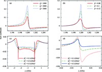
To explore the phenomenon above more carefully,we further show the optical Kerr coefficient Reχ(3) as functions of Δ s at the case of on-resonance (Δ c =0) under different parameters regime. Figure 6(a) shows that the optical Kerr coefficient peak increases monotonously with the quality factor Q of the MoS2 resonator,i.e. the long vibration lifetime of the resonator will induce observably Kerr coefficient. In Figure 6(b),the larger the coupling strength is,the higher the optical Kerr coefficient peak will be. Since the optical Kerr coefficient peak is caused by the exciton-resonator coupling,the peak will become more and more obvious when the coupling is made stronger. These results demonstrate that the coupling plays a key role in such a coupled system. Switching the pump-exciton detuning to the case of pump off-resonant Δ cm,we demonstrate that the intensity of the pump laser will also affect the optical Kerr effect of the MoS2 resonator system. Figure 6(c) presents the optical Kerr coefficient as functions of Δ s at pump off-resonant Δ cm with different Rabi frequencies of the pump laser,and the details are shown in Figure 6(d). We notice that the probe field experiences different optical Kerr coefficients with different pump laser intensities. Focusing on the detail,the optical Kerr effect will be weakened significantly via increasing the intensity of the pump laser. Therefore,the magnitude of optical Kerr effect can be tuned by controlling the pump intensity,which presents a method for modifying the nonlinear optical features of MoS2 resonator via coupling to the exciton in the system.

Figure  6.  (Color online) The optical Kerr coefficient as functions of probe-exciton detuning Δ s under (a) three quality factor Q of the resonator and (b) three exciton-resonator coupling β at pump field on resonant Δ c =0. (c) show the optical Kerr coefficient as functions of probe-exciton detuning Δ s with several different Rabi frequencies at pump laser off-resonance (Δ cm,and (d) indicates the detailed part of (c).

We have theoretically proposed a nano-optomechanical system based on monolayer MoS2 with optical pump-probe scheme. We investigate the coherent optical properties of this system,and the exciton-resonator coupling plays a key role which induces the phenomenon of phonon-induced transparency and significant nonlinear optical Kerr effect. The dispersion of the probe light in the case of the blue sideband may indicate the potential of ultraslow light and the possibility of superluminal light based on the coupled monolayer MoS2 resonator system. The phenomena of electromagnetically-induced absorption and parametric amplification are also demonstrated,and the monolayer MoS2 resonator system can work as an optical transistor,in which the pump field serves as a gate field which can effectively control the transmission of the probe field via regulating its power. Further,the high quality factor of the resonator and big exciton-resonator coupling strength will result in remarkable optical Kerr effect. By switching the pump-exciton detuning and manipulating the intensity of the pump laser,the optical Kerr effect of the system can be tuned. Our study,therefore,will indicate a new avenue for fabricating nanomechanical resonator systems based on layered nanomaterials and paves the way for various applications in nonlinear optics,quantum optics,and slow light devices.


[1]
Neto A H C, Guinea F, Peres N M R, et al. The electronic properties of graphene. Rev Mod Phys, 2009, 81(1):109 doi: 10.1103/RevModPhys.81.109
[2]
Chen C, Rosenblatt S, Bolotin K I, et al. Performance of monolayer graphene nanomechanical resonators with electrical readout. Nature Nanotechnology, 2009, 4(12):861 doi: 10.1038/nnano.2009.267
[3]
Ganatra R, Zhang Q. Few-layer MoS2:a promising layered semiconductor. ACS Nano, 2014, 8(5):4074 doi: 10.1021/nn405938z
[4]
Mak K F, Lee C, Hone J, et al. Atomically thin MoS2:a new direct-gap semiconductor. Phys Rev Lett, 2010, 105(13):136805 doi: 10.1103/PhysRevLett.105.136805
[5]
He K, Poole C, Mak K F, et al. Experimental demonstration of continuous electronic structure tuning via strain in atomically thin MoS2. Nano Lett, 2013, 13(6):2931 doi: 10.1021/nl4013166
[6]
Eda G, Yamaguchi H, Voiry D, et al. Photoluminescence from chemically exfoliated MoS2. Nano Lett, 2011, 11(12):5111 doi: 10.1021/nl201874w
[7]
Lee H S, Min S W, Chang Y G, et al. MoS2 nanosheet phototransistors with thickness modulated optical energy gap. Nano Lett, 2012, 12(7):3695 doi: 10.1021/nl301485q
[8]
Lopez-Sanchez O, Lembke D, Kayci M, et al. Ultrasensitive photodetectors based on monolayer MoS2. Nat Nanotechnol, 2013, 8(7):497 doi: 10.1038/nnano.2013.100
[9]
Fontana M, Deppe T, Boyd A K, et al. Electron-hole transport and photovoltaic effect in gated MoS2 Schottky junctions. Sci Rep, 2013, 3, 1634 http://cn.bing.com/academic/profile?id=1974974080&encoded=0&v=paper_preview&mkt=zh-cn
[10]
Radisavljevic B, Radenovic A, Brivio J, et al. Single-layer MoS2 transistors. Nat Nanotechnol, 2011, 6(3):147 doi: 10.1038/nnano.2010.279
[11]
Krasnozhon D, Lembke D, Nyffeler C, et al. MoS2 transistors operating at gigahertz frequencies. Nano Lett, 2014, 14(10):5905 doi: 10.1021/nl5028638
[12]
Li H, Yin Z, He Q, et al. Fabrication of single-and multilayer MoS2 film-based field-effect transistors for sensing NO at room temperature. Small, 2012, 8(1):63 doi: 10.1002/smll.201101016
[13]
Perkins F K, Friedman A L, Cobas E, et al. Chemical vapor sensing with monolayer MoS2. Nano Lett, 2013, 13(2):668 doi: 10.1021/nl3043079
[14]
Liu B, Chen L, Liu G, et al. High-performance chemical sensing using Schottky-contacted chemical vapor deposition grown monolayer MoS2 transistors. ACS Nano, 2014, 8(5):5304 doi: 10.1021/nn5015215
[15]
Weber P, Guttinger J, Tsioutsios I, et al. Coupling graphene mechanical resonators to superconducting microwave cavities. Nano Lett, 2014, 14(5):2854 doi: 10.1021/nl500879k
[16]
Singh V, Bosman S J, Schneider B H, et al. Optomechanical coupling between a multilayer graphene mechanical resonator and a superconducting microwave cavity. Nat Nanotechnol, 2014, 9(10):820 doi: 10.1038/nnano.2014.168
[17]
Lee J, Wang Z, He K, et al. High frequency MoS2 nanomechanical resonators. ACS Nano, 2013, 7(7):6086 doi: 10.1021/nn4018872
[18]
van Leeuwen R, Castellanos-Gomez A, Steele G A, et al. Time-domain response of atomically thin MoS2 nanomechanical resonators. Appl Phys Lett, 2014, 105(4):041911 doi: 10.1063/1.4892072
[19]
Castellanos-Gomez A, van Leeuwen R, Buscema M, et al. Single-layer MoS2 mechanical resonators. Adv Mater, 2013, 25(46):6719 doi: 10.1002/adma.v25.46
[20]
Bertolazzi S, Brivio J, Kis A. Stretching and breaking of ultrathin MoS2. ACS Nano, 2011, 5(12):9703 doi: 10.1021/nn203879f
[21]
Castellanos-Gomez A, Poot M, Steele G A, et al. Elastic properties of freely suspended MoS2 nanosheets. Adv Mater, 2012, 24(6):772 doi: 10.1002/adma.201103965
[22]
Lee C, Yan H, Brus L E, et al. Anomalous lattice vibrations of single-and few-layer MoS2. ACS Nano, 2010, 4(5):2695 doi: 10.1021/nn1003937
[23]
Kioseoglou G, Hanbicki A T, Currie M, et al. Valley polarization and intervalley scattering in monolayer MoS2. Appl Phys Lett, 2012, 101(22):221907 doi: 10.1063/1.4768299
[24]
Molina-Sanchez A, Wirtz L. Phonons in single-layer and few-layer MoS2 and WS2. Phys Rev B, 2011, 84(15):155413 doi: 10.1103/PhysRevB.84.155413
[25]
Li T. Ideal strength and phonon instability in single-layer MoS2. Phys Rev B, 2012, 85(23):235407 doi: 10.1103/PhysRevB.85.235407
[26]
Wang Z, Lee J, He K, et al. Embracing structural nonidealities and asymmetries in two dimensional nanomechanical resonators. Sci Rep, 2014, 4:3919 http://cn.bing.com/academic/profile?id=2128957616&encoded=0&v=paper_preview&mkt=zh-cn
[27]
Suzuki H, Yamaguchi N, Izumi H. Theoretical and experimental studies on the resonance frequencies of a stretched circular plate:application to Japanese drum diaphragms. Acoust Sci Technol, 2009, 30(5):348 doi: 10.1250/ast.30.348
[28]
Chen H J, Zhu K D. Coherent optical responses and their application in biomolecule mass sensing based on a monolayer MoS2 nanoresonator. J Opt Soc Am B, 2014, 31(7):1684 doi: 10.1364/JOSAB.31.001684
[29]
Li J J, Zhu K D. All-optical mass sensing with coupled mechanical resonator systems. Phys Rep, 2013, 525(3):223 doi: 10.1016/j.physrep.2012.11.003
[30]
Xu X, Sun B, Berman P R, et al. Coherent optical spectroscopy of a strongly driven quantum dot. Science, 2007, 317(5840):929 doi: 10.1126/science.1142979
[31]
Chen H J, Zhu K D. Graphene-based nanoresonator with applications in optical transistor and mass sensing. Sensors, 2014, 14(9):16740 doi: 10.3390/s140916740
[32]
Safavi-Naeini A H, Alegre T P M, Chan J, et al. Electromagnetically induced transparency and slow light with optomechanics. Nature, 2011, 472(7341):69 doi: 10.1038/nature09933
[33]
Okamoto H, Gourgout A, Chang C Y, et al. Coherent phonon manipulation in coupled mechanical resonators. Nat Phys, 2013, 9(8):480 doi: 10.1038/nphys2665
[34]
Yan H, Low T, Guinea F, et al. Tunable phonon-induced transparency in bilayer grapheme nanoribbons. Nano Lett, 2014, 14(8):4581 doi: 10.1021/nl501628x
Fig. 1.  (Color online) (a) The proposed setup of monolayer MoS2-based nanomechanical resonator suspended on the Si/SiO2 substrate with the optical pump-probe technique. (b) Molecular structure of MoS2. (c) The energy-level diagram of exciton in the MoS2 coupled to the resonator.

Fig. 2.  (Color online) (a) The imaginary and real part of the linear optical susceptibility as a function of the probe-exciton detuning Δ s at the pump field on-resonant Δ c =0. (b) The imaginary and real part of the linear optical susceptibility as a function of Δ s under off-resonant Δ cm. (c) The transmission of the probe laser as a function of Δ s without (β =0) and with (β =0.1) the exciton-resonator coupling.

Fig. 3.  (Color online) (a) The absorption spectrum as a function of signal-exciton detuning Δ s in the case of pump field off-resonance Δ cm (red curve) and Δ c =-ω m (green curve),respectively. (b) The dispersion spectrum as a function of Δ s under pump field off-resonance Δ cm (red curve) and Δ c =-ω m (green curve),respectively.

Fig. 4.  The probe transmission spectrum as a function of probe-exciton detuning Δ s for several different control field powers at Δ c =-ω m,respectively. (h) Amplification of the probe field around the region Δ s=0 for three different control powers with Δ c =-ω m.

Fig. 5.  (Color online) The optical Kerr coefficient and nonlinear absorption as functions of probe-exciton detuning Δ s without the exciton-resonator coupling (β =0) in (a) and with the exciton-resonator coupling (β =0.1) in (b),respectively.

Fig. 6.  (Color online) The optical Kerr coefficient as functions of probe-exciton detuning Δ s under (a) three quality factor Q of the resonator and (b) three exciton-resonator coupling β at pump field on resonant Δ c =0. (c) show the optical Kerr coefficient as functions of probe-exciton detuning Δ s with several different Rabi frequencies at pump laser off-resonance (Δ cm,and (d) indicates the detailed part of (c).

[1]
Neto A H C, Guinea F, Peres N M R, et al. The electronic properties of graphene. Rev Mod Phys, 2009, 81(1):109 doi: 10.1103/RevModPhys.81.109
[2]
Chen C, Rosenblatt S, Bolotin K I, et al. Performance of monolayer graphene nanomechanical resonators with electrical readout. Nature Nanotechnology, 2009, 4(12):861 doi: 10.1038/nnano.2009.267
[3]
Ganatra R, Zhang Q. Few-layer MoS2:a promising layered semiconductor. ACS Nano, 2014, 8(5):4074 doi: 10.1021/nn405938z
[4]
Mak K F, Lee C, Hone J, et al. Atomically thin MoS2:a new direct-gap semiconductor. Phys Rev Lett, 2010, 105(13):136805 doi: 10.1103/PhysRevLett.105.136805
[5]
He K, Poole C, Mak K F, et al. Experimental demonstration of continuous electronic structure tuning via strain in atomically thin MoS2. Nano Lett, 2013, 13(6):2931 doi: 10.1021/nl4013166
[6]
Eda G, Yamaguchi H, Voiry D, et al. Photoluminescence from chemically exfoliated MoS2. Nano Lett, 2011, 11(12):5111 doi: 10.1021/nl201874w
[7]
Lee H S, Min S W, Chang Y G, et al. MoS2 nanosheet phototransistors with thickness modulated optical energy gap. Nano Lett, 2012, 12(7):3695 doi: 10.1021/nl301485q
[8]
Lopez-Sanchez O, Lembke D, Kayci M, et al. Ultrasensitive photodetectors based on monolayer MoS2. Nat Nanotechnol, 2013, 8(7):497 doi: 10.1038/nnano.2013.100
[9]
Fontana M, Deppe T, Boyd A K, et al. Electron-hole transport and photovoltaic effect in gated MoS2 Schottky junctions. Sci Rep, 2013, 3, 1634 http://cn.bing.com/academic/profile?id=1974974080&encoded=0&v=paper_preview&mkt=zh-cn
[10]
Radisavljevic B, Radenovic A, Brivio J, et al. Single-layer MoS2 transistors. Nat Nanotechnol, 2011, 6(3):147 doi: 10.1038/nnano.2010.279
[11]
Krasnozhon D, Lembke D, Nyffeler C, et al. MoS2 transistors operating at gigahertz frequencies. Nano Lett, 2014, 14(10):5905 doi: 10.1021/nl5028638
[12]
Li H, Yin Z, He Q, et al. Fabrication of single-and multilayer MoS2 film-based field-effect transistors for sensing NO at room temperature. Small, 2012, 8(1):63 doi: 10.1002/smll.201101016
[13]
Perkins F K, Friedman A L, Cobas E, et al. Chemical vapor sensing with monolayer MoS2. Nano Lett, 2013, 13(2):668 doi: 10.1021/nl3043079
[14]
Liu B, Chen L, Liu G, et al. High-performance chemical sensing using Schottky-contacted chemical vapor deposition grown monolayer MoS2 transistors. ACS Nano, 2014, 8(5):5304 doi: 10.1021/nn5015215
[15]
Weber P, Guttinger J, Tsioutsios I, et al. Coupling graphene mechanical resonators to superconducting microwave cavities. Nano Lett, 2014, 14(5):2854 doi: 10.1021/nl500879k
[16]
Singh V, Bosman S J, Schneider B H, et al. Optomechanical coupling between a multilayer graphene mechanical resonator and a superconducting microwave cavity. Nat Nanotechnol, 2014, 9(10):820 doi: 10.1038/nnano.2014.168
[17]
Lee J, Wang Z, He K, et al. High frequency MoS2 nanomechanical resonators. ACS Nano, 2013, 7(7):6086 doi: 10.1021/nn4018872
[18]
van Leeuwen R, Castellanos-Gomez A, Steele G A, et al. Time-domain response of atomically thin MoS2 nanomechanical resonators. Appl Phys Lett, 2014, 105(4):041911 doi: 10.1063/1.4892072
[19]
Castellanos-Gomez A, van Leeuwen R, Buscema M, et al. Single-layer MoS2 mechanical resonators. Adv Mater, 2013, 25(46):6719 doi: 10.1002/adma.v25.46
[20]
Bertolazzi S, Brivio J, Kis A. Stretching and breaking of ultrathin MoS2. ACS Nano, 2011, 5(12):9703 doi: 10.1021/nn203879f
[21]
Castellanos-Gomez A, Poot M, Steele G A, et al. Elastic properties of freely suspended MoS2 nanosheets. Adv Mater, 2012, 24(6):772 doi: 10.1002/adma.201103965
[22]
Lee C, Yan H, Brus L E, et al. Anomalous lattice vibrations of single-and few-layer MoS2. ACS Nano, 2010, 4(5):2695 doi: 10.1021/nn1003937
[23]
Kioseoglou G, Hanbicki A T, Currie M, et al. Valley polarization and intervalley scattering in monolayer MoS2. Appl Phys Lett, 2012, 101(22):221907 doi: 10.1063/1.4768299
[24]
Molina-Sanchez A, Wirtz L. Phonons in single-layer and few-layer MoS2 and WS2. Phys Rev B, 2011, 84(15):155413 doi: 10.1103/PhysRevB.84.155413
[25]
Li T. Ideal strength and phonon instability in single-layer MoS2. Phys Rev B, 2012, 85(23):235407 doi: 10.1103/PhysRevB.85.235407
[26]
Wang Z, Lee J, He K, et al. Embracing structural nonidealities and asymmetries in two dimensional nanomechanical resonators. Sci Rep, 2014, 4:3919 http://cn.bing.com/academic/profile?id=2128957616&encoded=0&v=paper_preview&mkt=zh-cn
[27]
Suzuki H, Yamaguchi N, Izumi H. Theoretical and experimental studies on the resonance frequencies of a stretched circular plate:application to Japanese drum diaphragms. Acoust Sci Technol, 2009, 30(5):348 doi: 10.1250/ast.30.348
[28]
Chen H J, Zhu K D. Coherent optical responses and their application in biomolecule mass sensing based on a monolayer MoS2 nanoresonator. J Opt Soc Am B, 2014, 31(7):1684 doi: 10.1364/JOSAB.31.001684
[29]
Li J J, Zhu K D. All-optical mass sensing with coupled mechanical resonator systems. Phys Rep, 2013, 525(3):223 doi: 10.1016/j.physrep.2012.11.003
[30]
Xu X, Sun B, Berman P R, et al. Coherent optical spectroscopy of a strongly driven quantum dot. Science, 2007, 317(5840):929 doi: 10.1126/science.1142979
[31]
Chen H J, Zhu K D. Graphene-based nanoresonator with applications in optical transistor and mass sensing. Sensors, 2014, 14(9):16740 doi: 10.3390/s140916740
[32]
Safavi-Naeini A H, Alegre T P M, Chan J, et al. Electromagnetically induced transparency and slow light with optomechanics. Nature, 2011, 472(7341):69 doi: 10.1038/nature09933
[33]
Okamoto H, Gourgout A, Chang C Y, et al. Coherent phonon manipulation in coupled mechanical resonators. Nat Phys, 2013, 9(8):480 doi: 10.1038/nphys2665
[34]
Yan H, Low T, Guinea F, et al. Tunable phonon-induced transparency in bilayer grapheme nanoribbons. Nano Lett, 2014, 14(8):4581 doi: 10.1021/nl501628x
1

Simulation of MoS2 stacked nanosheet field effect transistor

Yang Shen, He Tian, Tianling Ren

Journal of Semiconductors, 2022, 43(8): 082002. doi: 10.1088/1674-4926/43/8/082002

2

Charge transport and quantum confinement in MoS2 dual-gated transistors

Fuyou Liao, Hongjuan Wang, Xiaojiao Guo, Zhongxun Guo, Ling Tong, et al.

Journal of Semiconductors, 2020, 41(7): 072904. doi: 10.1088/1674-4926/41/7/072904

3

Differential optical gain in a GaInN/AlGaN quantum dot

K. Jaya Bala, A. John Peter

Journal of Semiconductors, 2017, 38(6): 062001. doi: 10.1088/1674-4926/38/6/062001

4

Manganese and chromium doping in atomically thin MoS2

Ce Huang, Yibo Jin, Weiyi Wang, Lei Tang, Chaoyu Song, et al.

Journal of Semiconductors, 2017, 38(3): 033004. doi: 10.1088/1674-4926/38/3/033004

5

Effect of Co doping on structural, optical, electrical and thermal properties of nanostructured ZnO thin films

Sonet Kumar Saha, M. Azizar Rahman, M. R. H. Sarkar, M. Shahjahan, M. K. R. Khan, et al.

Journal of Semiconductors, 2015, 36(3): 033004. doi: 10.1088/1674-4926/36/3/033004

6

Electro-magnetic weak coupling optical polaron and temperature effect in quantum dot

M. Tiotsop, A. J. Fotue, S. C. Kenfack, N. Issofa, A. V. Wirngo, et al.

Journal of Semiconductors, 2015, 36(10): 102001. doi: 10.1088/1674-4926/36/10/102001

7

Theoretical study of defect impact on two-dimensional MoS2

Anna V. Krivosheeva, Victor L. Shaposhnikov, Victor E. Borisenko, Jean-Louis Lazzari, Chow Waileong, et al.

Journal of Semiconductors, 2015, 36(12): 122002. doi: 10.1088/1674-4926/36/12/122002

8

Correlation between electrical conductivity-optical band gap energy and precursor molarities ultrasonic spray deposition of ZnO thin films

Said Benramache, Okba Belahssen, Abderrazak Guettaf, Ali Arif

Journal of Semiconductors, 2013, 34(11): 113001. doi: 10.1088/1674-4926/34/11/113001

9

Dielectric confinement on exciton binding energy and nonlinear optical properties in a strained Zn1-xinMgxinSe/Zn1-xoutMgxoutSe quantum well

J. Abraham Hudson Mark, A. John Peter

Journal of Semiconductors, 2012, 33(9): 092001. doi: 10.1088/1674-4926/33/9/092001

10

Optical and electrical properties of electrochemically deposited polyaniline-CeO2 hybrid nanocomposite film

Anees A. Ansari, M. A. M. Khan, M. Naziruddin Khan, Salman A. Alrokayan, M. Alhoshan, et al.

Journal of Semiconductors, 2011, 32(4): 043001. doi: 10.1088/1674-4926/32/4/043001

11

Optical and structural properties of sol–gel derived nanostructured CeO2 film

Anees A. Ansari

Journal of Semiconductors, 2010, 31(5): 053001. doi: 10.1088/1674-4926/31/5/053001

12

Mode analysis and structure parameter optimization of a novel SiGe-OI rib optical waveguide

Feng Song, Gao Yong, Yang Yuan, Feng Yuchun

Journal of Semiconductors, 2009, 30(8): 084008. doi: 10.1088/1674-4926/30/8/084008

13

Optical and electrical properties of N-doped ZnO and fabrication of thin-film transistors

Zhu Xiaming, Wu Huizhen, Wang Shuangjiang, Zhang Yingying, Cai Chunfeng, et al.

Journal of Semiconductors, 2009, 30(3): 033001. doi: 10.1088/1674-4926/30/3/033001

14

A monolithic, standard CMOS, fully differential optical receiver with an integrated MSM photodetector

Yu Changliang, Mao Luhong, Xiao Xindong, Xie Sheng, Zhang Shilin, et al.

Journal of Semiconductors, 2009, 30(10): 105010. doi: 10.1088/1674-4926/30/10/105010

15

A 1.5 Gb/s monolithically integrated optical receiver in the standard CMOS process

Xiao Xindong, Mao Luhong, Yu Changliang, Zhang Shilin, Xie Sheng, et al.

Journal of Semiconductors, 2009, 30(12): 125004. doi: 10.1088/1674-4926/30/12/125004

16

Growth and Optical Properties of ZnO Films and Quantum Wells

Zhang Baoping, Kang Junyong, Yu Jinzhong, Wang Qiming, Segawa Yusaburo, et al.

Chinese Journal of Semiconductors , 2006, 27(4): 613-622.

17

An Evanescent Coupling Approach for Optical Characterization of ZnO Nanowires

Yang Qing, Lou Jingyi, Yang Deren, Tong Limin

Chinese Journal of Semiconductors , 2006, 27(3): 425-428.

18

30Gbit/s Parallel Optical Receiver Module

Chen Hongda, Jia Jiuchun, Pei Weihua, Tang Jun

Chinese Journal of Semiconductors , 2006, 27(4): 696-699.

19

A 1×4 Polymeric Digital Optical Switch Basedon the Thermo-Optic Effect

Tang Yi, Zhang Hao, Yang Jianyi, Wang Minghua, Jiang Xiaoqing, et al.

Chinese Journal of Semiconductors , 2006, 27(4): 692-695.

20

Effect of Surface-Covered Annealing on the Optical Properties of ZnO Films Grown by MOCVD

Wang Li, Pu Yong, Fang Wenqing, Mo Chunlan, Xiong Chuanbing, et al.

Chinese Journal of Semiconductors , 2003, 24(3): 409-412.

  • Search

    Advanced Search >>

    GET CITATION

    Huajun Chen, Changzhao Chen, Yang Li, Xianwen Fang. Monolayer-molybdenum-disulfide-based nano-optomechanical transistor andewline tunable nonlinear responses[J]. Journal of Semiconductors, 2016, 37(11): 114004. doi: 10.1088/1674-4926/37/11/114004
    H J Chen, C Z Chen, Y Li, X W Fang. Monolayer-molybdenum-disulfide-based nano-optomechanical transistor andewline tunable nonlinear responses[J]. J. Semicond., 2016, 37(11): 114004. doi: 10.1088/1674-4926/37/11/114004.
    shu

    Export: BibTex EndNote

    Article Metrics

    Article views: 2801 Times PDF downloads: 19 Times Cited by: 0 Times

    History

    Received: 03 March 2016 Revised: 20 May 2016 Online: Published: 01 November 2016

    Catalog

      Email This Article

      User name:
      Email:*请输入正确邮箱
      Code:*验证码错误
      Huajun Chen, Changzhao Chen, Yang Li, Xianwen Fang. Monolayer-molybdenum-disulfide-based nano-optomechanical transistor andewline tunable nonlinear responses[J]. Journal of Semiconductors, 2016, 37(11): 114004. doi: 10.1088/1674-4926/37/11/114004 ****H J Chen, C Z Chen, Y Li, X W Fang. Monolayer-molybdenum-disulfide-based nano-optomechanical transistor andewline tunable nonlinear responses[J]. J. Semicond., 2016, 37(11): 114004. doi: 10.1088/1674-4926/37/11/114004.
      Citation:
      Huajun Chen, Changzhao Chen, Yang Li, Xianwen Fang. Monolayer-molybdenum-disulfide-based nano-optomechanical transistor andewline tunable nonlinear responses[J]. Journal of Semiconductors, 2016, 37(11): 114004. doi: 10.1088/1674-4926/37/11/114004 ****
      H J Chen, C Z Chen, Y Li, X W Fang. Monolayer-molybdenum-disulfide-based nano-optomechanical transistor andewline tunable nonlinear responses[J]. J. Semicond., 2016, 37(11): 114004. doi: 10.1088/1674-4926/37/11/114004.

      Monolayer-molybdenum-disulfide-based nano-optomechanical transistor andewline tunable nonlinear responses

      DOI: 10.1088/1674-4926/37/11/114004
      Funds:

      National Natural Science Foundation of China Nos. 11404005, 51502005, 61272153, 61572035

      Project supported by the National Natural Science Foundation of China (Nos. 11404005, 51502005, 61272153, 61572035), the Key Foundation for Young Talents in College of Anhui Province (No. 2013SQRL026ZD), and the Foundation for PhD in Anhui University of Science and Technology.

      Key Foundation for Young Talents in College of Anhui Province No. 2013SQRL026ZD

      Foundation for PhD in Anhui University of Science and Technology 

      More Information
      • Corresponding author: Chen Huajun,chenphysics@126.com
      • Received Date: 2016-03-03
      • Revised Date: 2016-05-20
      • Published Date: 2016-11-01

      Catalog

        /

        DownLoad:  Full-Size Img  PowerPoint
        Return
        Return