Processing math: 100%
J. Semicond. > 2016, Volume 37 > Issue 2 > 022002

SEMICONDUCTOR PHYSICS

Impact of stray charge on interconnect wire via probability model of double-dot system

Xiangye Chen1, , Li Cai2, Qiang Zeng1 and Xinqiao Wang1

+ Author Affiliations

 Corresponding author: Xiangye Chen, Email: conquor_fighter@qq.com

DOI: 10.1088/1674-4926/37/2/022002

PDF

Abstract: 
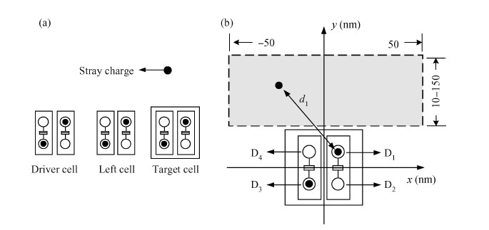
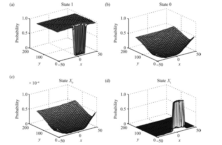
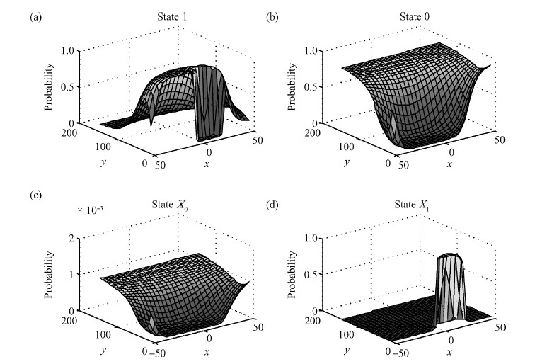
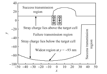
The behavior of quantum cellular automata (QCA) under the influence of a stray charge is quantified. A new time-independent switching paradigm, a probability model of the double-dot system, is developed. Superiority in releasing the calculation operation is presented by the probability model compared to previous stray charge analysis utilizing ICHA or full-basis calculation. Simulation results illustrate that there is a 186-nm-wide region surrounding a QCA wire where a stray charge will cause the target cell to switch unsuccessfully. The failure is exhibited by two new states' dominating the target cell. Therefore, a bistable saturation model is no longer applicable for stray charge analysis.

Key words: quantum cellular automatainterconnect wirestray chargeprobability model of double-dot system

Quantum-dot cellular automata (QCA) is a promising device that uses electron repulsion,instead of current,to create bistable behavior in electrostatically linked cells via a nanoscale architecture[1, 2, 3, 4, 5]. This special mechanism makes it possible to achieve circuit densities and clock frequencies beyond the limits of existing CMOS technology[5, 6, 7]. Those advantages accelerate QCA becoming one of the candidates to replace today's silicon circuitry[7, 8, 9, 10]. QCA devices have shown great promise to be faster and smaller than conventional microelectronic devices,and to operate at a fraction of the power[6]. Besides,the QCA cell,majority,lines and fanout have been realized in laboratory[11, 12, 13, 14].

However,QCA cells are also faced with challenges to provide reliable logic operations[15, 16, 17, 18, 19]. Since the information in a QCA system is encoded and propagated by the states of the individual cells,these systems are particularly never free from background charges introduced into the system by material defects. Unfortunately,these stray charges can cause a very significant effect on the system behavior. Moreover,they even result in complete failure if located in an undesirable location. Though consideration of the effects of fabrication errors and fault tolerance is an important topic of work in QCA research,papers conducted to study the effect of stray charges remain lacking. Yakimenko \textit{et al.} showed interest in time-dependent behavior of QCA with imperfections including stray charges resumptively[20]. Lent \textit{et al.} also devoted special attention to analyze stray charge on molecular quantum-dot cellular automata[4]. Taugaw \textit{et al.} analyzed stray charges in QCA using the intercellular Hartree approximation (ICHA)[21, 22]. The knowledge gained by these studies revealed that stray charge might destroy the expected switching of the cell at a certain degree. However,simulation methods,especially full-basis calculation,were complex and required high computer performance. Therefore,to analyze the affection of stray charge on bigger system seems impossible.

In this paper,a novel paradigm for stray charge analysis is proposed. Then we perform this paradigm in order to analyze the behavior of the QCA line with the presence of a stray charge. The technique is based on the schematic diagram of a QCA cell presented in Reference [23]. A cell is regarded as the combination of two double-dot (DD) systems proposed in Reference [11]. The Hamiltonian of each DD is calculated to achieve the probability of the cell being at the correct state. We define this technique as the probability model of the double-dot system. By performing this model,simulations obtained revealed that there was a 186-nm-wide region surrounding a QCA wire where a stray charge will cause the target cell to switch unsuccessfully. When the failure transmission is taken out,two new states are exhibited by QCA cells. Bistable saturation is no longer applicable for stray charge analysis. A probability model has demonstrated its validity based on the consistent simulation results with previous research in Reference~[22].

The remainder of this work is organized as follows. In Section 2,QCA cells and the computation method are presented. In Section 3,the probability model of the double-dot system for QCA for stray charge analysis is developed in detail. We perform the probability model to simulate and analyze the effect of stray charge on an interconnect wire in Section 4. In the following section,we briefly make an operation complexity comparison among the probability model,ICHA,and full-basis calculation. Section 6 concludes the paper.

A functioning QCA cell has been realized by Orlov in Reference [11]. The double-dot (DD) system is the computing model of the realized QCA cell[23]. Shown in Figure 1(a),the device consists of four Al islands,with input dots D1 and D2 and output dots D3 and D4. The Al-AlOx-Al tunnel junctions were fabricated on an oxidized Si substrate[11]. The size of the cell is about 20 nm and the distance between two cells is 40~nm. The sample was mounted on the cold finger of a dilution refrigerator with a base temperature of 15 mK. Capacitances lie between D1-D3 and D2-D4,and junctions lie between D1-D2 and D3-D4. Therefore,electron tunneling would exist between D1-D2 and D3-D4. No tunneling exists between D1-D3 or D2-D4. According to this mechanism,a QCA cell could be divided into two DDs shown in Figure 1(b). The left DD acts as part of the input of the right cell. Meanwhile,the right DD is made up of the input of the next whole cell.

Figure  1.  (a) Schematic diagram of an integrated cell[11]. (b) A two double-dot system consisting of an integrated cell[23].

We model the integrated cell shown using a Hubbard-type Hamiltonian[1]. For an isolated cell,the Hamiltonian can be written

Hcell0=i,δE0,ini,δ+i,δt(ai,δ\daga0,δ+a0,δ\dagai,δ)+iEQni,ni,+i>j,δ,δVQni,δnj,δ|RiRj|.

(1)

Here,ai,δ is the annihilation operator which destroys a particle at site i (i= 0,1,2,3,4) with spin δ. The number operator for site i and spin δ is represented by ni,δ. E0,i stands for the on-site energy of the i-th dot; the coupling to the central dot is t; and the charging energy for a single dot is EQ. The last term represents the Coulombic potential energy for two electrons located at sites i and j at positions Ri and Rj; the Coulomb coupling strength is VQ.

In this section,the technique of the probability model is presented in detail. Radically,the probability model prefers to obtain the probabilities of states that an integrated cell exhibits. Since each DD has only two states,the number of states exhibited by the integrated cell will be four. We firstly calculate the Hamiltonian of the target DD. When the Hamiltonian is gained,all probabilities of the target DD can be reached by solving a time-independent Schrodinger equation.

Figure 2 shows a target cell and its driver cell. At an initial moment,the state of the driver cell changes to `1' from `0'. Meanwhile,a stray electron presents instantly. On this occasion,the Hamiltonian of the target DD is the summation of three parts: the Hamiltonian of an isolated DD (denoted as Hcell0),the Hamiltonian arises from driver cells (denoted as Hdriver),and the Hamiltonian arises from the stray charge (denoted as Hcharge):

Figure  2.  Schematic diagram of a target DD and its driver cells.

Hcell=Hcell0+Hdriver+Hcharge.

(2)

Two conditions are pointed out clearly here: (1) an integrated cell is pictured as one left DD and one right DD shown in Figure 2; and (2) how to confirm a DD's input components conforms to certain rules. For a left DD,its drivers only consist of the anterior integrated cell; but for a right DD,the drivers consist of the anterior integrated cell and the left DD. For instance as shown in Figure 2,the input components of DD3 are DD1 and DD2; but the input components of DD4 are DD1,DD2 and DD3.

Hcell0,Hdriver and Hcharge have many commons in References [6, 24]:

Hcell0=[E0,1ttE0,2],

(3)

Hdriver=[Edriver00Edriver],

(4)

Hcharge=[Echarge00Echarge].

(5)

In the rest of the paper,we will consider the case in which all the on-site energies are equal,E0,i=E0. t represents the tunneling energy provided by the clock. Edriver and Echarge are similar to kink energy and can be gained as follows[6]:

Edriver=EoppositepolarizationdriverEsamepolarizationdriver,

(6)

Echarge=EoppositepolarizationchargeEsamepolarizationcharge,

(7)

where Eoppositepolarizationdriver stands for the Coulombic potential energy due to electrons of input cells and the electron on the expected dot of the target DD,and Esamepolarizationdriver represents the Coulombic potential energy caused by electrons of input cells and the electron on the unexpected dot of the target DD. Hence,we have

Epolarizationdriver=14πε0εrNi2jqiqjdij,N=4or6.

(8)

Here,N is selected as 4 if target DD is a left DD. Otherwise,N=6. qi is the charge of the i-th dot. dij represents the distance between the electrons on the i-th dot and j-th dot. ε0 is the permittivity of free space,and εr is relative permittivity. If stray charge is substituted for the electrons of input cells,we can gain:

Epolarizationcharge=e4πε0εr2jqjdj,

(9)

where dj is the distance between the stray charge and the electron in the target DD.

As can be seen from Figure 3(a),a DD cell with an electron on the top dot is defined to be at state `Φ0' (corresponding to |ϕ1),and on the bottom dot,to be at state `Φ1' (corresponding to |ϕ2). Therefore,four states will be exhibited by an integrated cell: `0',`1',`X0',`X1',shown in Figure 3(b).

Figure  3.  States in probability model. (a) Two states exhibited by a DD cell. (b) Four states exhibited by an integrated cell.

We solve the time-independent Schrodinger equation for the state of the system,|i,under the influence of the driver cells and stray charge[1]:

Hcell|i=Ei|i,i=1or2.

(10)

Solving Equation (10),we can gain the ground state of the cell in an adiabatic situation,|0. |0 is represented as[1]:

|0=α|ϕ1+β|ϕ2,

(11)

where |ϕ1 and |ϕ2 are two basis kets:

\begin{equation} \label{eq12} \vert \phi _1 \rangle =\vert 0 1\rangle , \end{equation} \begin{equation}

(12)

\label{eq13} \vert \phi _2 \rangle =\vert 10\rangle . \end{equation}

(13)

With the determination of |0left,the initial state can be expanded by a linear combination of |ϕ1,|ϕ2 (denote the coefficients as α1,β1). In the condition that the left DD of the target cell has switched to Φ0,two coefficients of the right DD at each state can be attained as α2,β2; otherwise (the left DD of the target cell has switched to Φ1),we have α2,β2. In quantum mechanics,α21,β21,α22,β22,α22 and β22 are corresponding probabilities of left DD and right DD to be at each state:

α21=P{DDleft=Φ0},

(14)

β21=P{DDleft=Φ1},

(15)

α22=P{DDright=Φ0|DDleft=Φ0},

(16)

β22=P{DDright=Φ1|DDleft=Φ0},

(17)

α22=P{DDright=Φ0|DDleft=Φ1},

(18)

β22=P{DDright=Φ1|DDleft=Φ1}.

(19)

Hence,probabilities of the target cell's four states can be achieved (denoting the target cell as C):

P\{C=0\}=\alpha _1^2  \beta _2^2 , \end{gather}

(20)

P{C=1}=β21α22,

(21)

P{C=X0}=α21α22,

(22)

P{C=X1}=β21β22.

(23)

As defined in Reference [1],four single-particle densities,ρ1,ρ2,ρ3,ρ4,can be computed:

ρ1=P{C=1}+P{C=X0},

(24)

ρ2=P{C=0}+P{C=X1},

(25)

ρ3=P{C=1}+P{C=X1},

(26)

ρ4=P{C=0}+P{C=X0}.

(27)

So we have the polarization,P,in a new format:

P=P{C=1}P{C=0}.

(28)

In this section,vast work has been conducted to build the probability model of the interconnect wire with the presence of a stray charge. According to the fact that the driver cell is fixed at `0' or `1',two paradigms will be developed. Simulations reveal that there is about a 186-nm-wide region surrounding the QCA wire where a stray charge will cause the wire to failure.

Figure 4(a) shows that the driver cell is fixed at `1'. The interconnect wire is consisted with two cells. A stray charge locates in the shadow region shown in Figure 4(b). Four dots of the target cell are denoted as D1,D2,D3 and D4. The distances between the stray charge and four dots are d1,d2,d3 and d4. For simplifying the model,a region ranging from -50 to 50~nm (along the direction of the x axis) and 10 to 150 nm (along the direction of the y axis) is taken into consideration in the rectangular plane coordinate system.

Figure  4.  Schematic diagram of a two cells wire.

To study the influence of stray charge,we change the coordinate of the electron in Figure 4(b),and monitor the variations of the performance of the target cell. In Figure 4(a),simulations are classified into two categories according to whether the driver cell is at `0' or `1' (actually,four cases exist,but only two are valuable because cases are symmetrical). In each case,some universal parameters are taken as following: E0= 4~meV,γ= 0.3 meV,the distance between two cells is 40~nm,the size of the cell is 20 nm,the relative dielectric constant,εr = 10.

A threshold should be chosen as a criterion to help us judge whether a cell can operate correctly or not. Reference [22] has illustrated that a cell cannot operate properly when its polarization fails to meet 0.5. As can be seen in Equation (28),when the target cell stays at state `1' with probability 75%,its polarization is certainly higher than 0.5. Thus,in the rest of the paper,the threshold is chosen as 75% (denoted as Pthreshold).

We calculate the probabilities of the target cell being at four states using the probability model. Figure 5 presents that the target cell is more likely to be at `1' (Figure 5(a)) or `X1' (Figure 5(d)) under the influences of left cell and stray charge. `0' and `X0' have low probabilities (below 0.1%) to appear in this case. Obviously,when the distance between the stray charge and the target cell increases,the influence of the stray charge declines smoothly. State `X1' appears at a higher probability in a certain region (5 nm < x < 25 nm,10 nm < y < 60 nm) (denoted as D). Correspondingly,state `1' is more likely to appear while the stray charge locates out of D. This is resulted by the strong mutual Coulombic repulsion of the electrons in dots and the stray charge. As the repulsion decreases,the affection of stray charge can be ignored. Figure 7 shows the region where the stray charge can cause a failure transmission.

Figure  5.  Target cell performance with the driver cell of ‘1’.

Switching the driver cell to state `0' makes the case more complicated. Figure 6 reveals that states `0',`1' and `X1' are the main states to be presented in this case. States `1' and `X1' have relatively high probabilities to occur in region A (5 nm < x < 25 nm,10 nm < y < 60 nm). In a narrow and small region A1 (5 nm < x < 25 nm,10 nm < y < 25 nm,around dot D1),the target cell will stay at `X1' with a probability nearby 100% (Figure 6(d)),while in the other region of A,the target cell will stay at `1' with a probability higher than 75% (Figure 6(a)). This phenomena is quite acceptant: in A1,the stray charge has erased the kink energies of the left integrated cell and the left DD,and makes the target cell switch to `X1'; in the other region of A,the stray charge accelerates the left DD to stay at `Φ1',but its influence becomes weaker to erase the kink of the left DD,which results that the right DD stays at `Φ0' and the target cell stays at `1'. A fail region can also be pictured in Figure 7. In this region,the target cell switches correctly with probabilities lower than Pthreshold.

Figure  6.  Target cell performance with the driver cell of ‘0’.

Figure 7 distinctly illustrates the stray charge affects the target cell. In this situation,the driver cell is fixed at `1',and the stray charge presents up or below the target cell. Two lines in Figure 7 differentiate the region whether a stray charge will cause a failure signal transmission or not: if a stray charge locates between the lines,a failure transmission takes out; otherwise,the influence of the stray charge can be ignored. The failure transmission region (between two lines) seems to be two half analogously elliptical regions. The biggest widths are at y= 30 nm and y=93 nm. Conclusively,a 186-nm-wide region will cause a failure signal transmission.

Figure  7.  Target cell performance with the driver cell of ‘0’.

Full-basis calculation and ICHA were separately presented in detail in References [24, 25]. The former can be used to calculate all the possible situations for a system,so the operation is O(16N),( if we apply six bias kets for one cell,the operation decreases but also remains at O(6N)). The ICHA method uses an iterative self-consistent calculation of single-cell Hamiltonians to determine stable states of the whole system. The stable state is highly dependent on the initial conditions used to begin the iterative calculation. Therefore,in order to confirm which state is the ground state,it is necessary to conduct several calculations with all different initial conditions. Additionally,in one calculation process,at least one iterative circle must be conducted. Therefore,if we assume that M stands for the number of initial conditions,and N is the maximum of iterative circle for each initial condition,the operation of the ICHA calculation is more than O(NM). As for the probability model,the operation is only O(M) if the aforesaid assumption is tenable. The superiority of the probability model is evident.

In this paper,the characteristics of QCA with the presence of a stray charge are studied. In addition,the method for stray charge analysis,the probability model,has been developed. A few observations and conclusions based on experiment simulations are as follows.


[1]
[2]
[3]
[4]
[5]
[6]
[7]
[8]
[9]
[10]
[11]
[12]
[13]
[14]
[15]
[16]
[17]
[18]
[19]
[20]
[21]
[22]
[23]
[24]
[25]
Fig. 1.  (a) Schematic diagram of an integrated cell[11]. (b) A two double-dot system consisting of an integrated cell[23].

Fig. 2.  Schematic diagram of a target DD and its driver cells.

Fig. 3.  States in probability model. (a) Two states exhibited by a DD cell. (b) Four states exhibited by an integrated cell.

Fig. 4.  Schematic diagram of a two cells wire.

Fig. 5.  Target cell performance with the driver cell of ‘1’.

Fig. 6.  Target cell performance with the driver cell of ‘0’.

Fig. 7.  Target cell performance with the driver cell of ‘0’.

[1]
[2]
[3]
[4]
[5]
[6]
[7]
[8]
[9]
[10]
[11]
[12]
[13]
[14]
[15]
[16]
[17]
[18]
[19]
[20]
[21]
[22]
[23]
[24]
[25]
1

A 130-nm ferroelectric nonvolatile system-on-chip for internet of things

Zhiyi Yu

Journal of Semiconductors, 2019, 40(2): 020205. doi: 10.1088/1674-4926/40/2/020205

2

An enhanced high-speed multi-digit BCD adder using quantum-dot cellular automata

D. Ajitha, K.V. Ramanaiah, V. Sumalatha

Journal of Semiconductors, 2017, 38(2): 024002. doi: 10.1088/1674-4926/38/2/024002

3

Donor impurity-related optical absorption coefficients and refractive index changes in a rectangular GaAs quantum dot in the presence of electric field

Sheng Wang, Yun Kang, Xianli Li

Journal of Semiconductors, 2016, 37(11): 112001. doi: 10.1088/1674-4926/37/11/112001

4

Performance analysis of charge plasma based dual electrode tunnel FET

Sunny Anand, S. Intekhab Amin, R. K. Sarin

Journal of Semiconductors, 2016, 37(5): 054003. doi: 10.1088/1674-4926/37/5/054003

5

Analysis of charge density and Fermi level of AlInSb/InSb single-gate high electron mobility transistor

S. Theodore Chandra, N. B. Balamurugan, M. Bhuvaneswari, N. Anbuselvan, N. Mohankumar, et al.

Journal of Semiconductors, 2015, 36(6): 064003. doi: 10.1088/1674-4926/36/6/064003

6

Electro-magnetic weak coupling optical polaron and temperature effect in quantum dot

M. Tiotsop, A. J. Fotue, S. C. Kenfack, N. Issofa, A. V. Wirngo, et al.

Journal of Semiconductors, 2015, 36(10): 102001. doi: 10.1088/1674-4926/36/10/102001

7

Analytical modeling and simulation of germanium single gate silicon on insulator TFET

T. S. Arun Samuel, N. B. Balamurugan

Journal of Semiconductors, 2014, 35(3): 034002. doi: 10.1088/1674-4926/35/3/034002

8

Analytical model for subthreshold current and subthreshold swing of short-channel double-material-gate MOSFETs with strained-silicon channel on silicon-germanium substrates

Pramod Kumar Tiwari, Gopi Krishna Saramekala, Sarvesh Dubey, Anand Kumar Mukhopadhyay

Journal of Semiconductors, 2014, 35(10): 104002. doi: 10.1088/1674-4926/35/10/104002

9

Model development for analyzing 2DEG sheet charge density and threshold voltage considering interface DOS for AlInN/GaN MOSHEMT

Devashish Pandey, T.R. Lenka

Journal of Semiconductors, 2014, 35(10): 104001. doi: 10.1088/1674-4926/35/10/104001

10

Modeling and simulation of centroid and inversion charge density in cylindrical surrounding gate MOSFETs including quantum effects

P. Vimala, N. B. Balamurugan

Journal of Semiconductors, 2013, 34(11): 114001. doi: 10.1088/1674-4926/34/11/114001

11

A CMOS AC/DC charge pump for a wireless sensor network

Zhang Qiang, Ni Weining, Shi Yin, Yu Yude

Journal of Semiconductors, 2012, 33(10): 105003. doi: 10.1088/1674-4926/33/10/105003

12

RF CMOS modeling: a scalable model of RF-MOSFET with different numbers of fingers

Yu Yuning, Sun Lingling, Liu Jun

Journal of Semiconductors, 2010, 31(11): 114007. doi: 10.1088/1674-4926/31/11/114007

13

A novel modified charge pumping method for trapped charge characterization in nanometer-scale devices

Zhu Peng, Pan Liyang, Gu Haiming, Qiao Fengying, Deng Ning, et al.

Journal of Semiconductors, 2010, 31(10): 104008. doi: 10.1088/1674-4926/31/10/104008

14

A low power cyclic ADC design for a wireless monitoring system for orthopedic implants

Chen Yi, Li Fule, Chen Hong, Zhang Chun, Wang Zhihua, et al.

Journal of Semiconductors, 2009, 30(8): 085009. doi: 10.1088/1674-4926/30/8/085009

15

Modeling and analysis of single-event transients in charge pumps

Zhao Zhenyu, Li Junfeng, Zhang Minxuan, Li Shaoqing

Journal of Semiconductors, 2009, 30(5): 055006. doi: 10.1088/1674-4926/30/5/055006

16

Accurate Interconnection Length and Routing Channel Width Estimates for FPGAs

Gao Haixia, Ma Xiaohua, Yang Yintang

Chinese Journal of Semiconductors , 2006, 27(7): 1196-1200.

17

Synthesis and Characterization of SiCOF/a-C∶F Double-Layer Films with Low Dielectric Constant for Copper Interconnects

Zhang Wei, Zhu Lian, Sun Qingqing, Lu Hongliang, Ding Shijin, et al.

Chinese Journal of Semiconductors , 2006, 27(3): 429-433.

18

1.3μm InGaAs/InAs/GaAs Self-Assembled Quantum Dot Laser Diode Grown by Molecular Beam Epitaxy

Niu Zhichuan, Ni Haiqiao, Fang Zhidan, Gong Zheng, Zhang Shiyong, et al.

Chinese Journal of Semiconductors , 2006, 27(3): 482-488.

19

Elmore Delay Estimation of Two Adjacent Coupling Interconnects

Dong Gang, Yang Yintang, Li Yuejin

Chinese Journal of Semiconductors , 2006, 27(1): 54-58.

20

Analytical Modeling of Threshold Voltage for Double-Gate MOSFET Fully Comprising Quantum Mechanical Effects

Zhang Dawei, Tian Lilin,and Yu Zhiping

Chinese Journal of Semiconductors , 2005, 26(3): 429-435.

  • Search

    Advanced Search >>

    GET CITATION

    Xiangye Chen, Li Cai, Qiang Zeng, Xinqiao Wang. Impact of stray charge on interconnect wire via probability model of double-dot system[J]. Journal of Semiconductors, 2016, 37(2): 022002. doi: 10.1088/1674-4926/37/2/022002
    X Y Chen, L Cai, Q Zeng, X Q Wang. Impact of stray charge on interconnect wire via probability model of double-dot system[J]. J. Semicond., 2016, 37(2): 022002. doi: 10.1088/1674-4926/37/2/022002.
    shu

    Export: BibTex EndNote

    Article Metrics

    Article views: 2604 Times PDF downloads: 11 Times Cited by: 0 Times

    History

    Received: 20 May 2015 Revised: Online: Published: 01 February 2016

    Catalog

      Email This Article

      User name:
      Email:*请输入正确邮箱
      Code:*验证码错误
      Xiangye Chen, Li Cai, Qiang Zeng, Xinqiao Wang. Impact of stray charge on interconnect wire via probability model of double-dot system[J]. Journal of Semiconductors, 2016, 37(2): 022002. doi: 10.1088/1674-4926/37/2/022002 ****X Y Chen, L Cai, Q Zeng, X Q Wang. Impact of stray charge on interconnect wire via probability model of double-dot system[J]. J. Semicond., 2016, 37(2): 022002. doi: 10.1088/1674-4926/37/2/022002.
      Citation:
      Xiangye Chen, Li Cai, Qiang Zeng, Xinqiao Wang. Impact of stray charge on interconnect wire via probability model of double-dot system[J]. Journal of Semiconductors, 2016, 37(2): 022002. doi: 10.1088/1674-4926/37/2/022002 ****
      X Y Chen, L Cai, Q Zeng, X Q Wang. Impact of stray charge on interconnect wire via probability model of double-dot system[J]. J. Semicond., 2016, 37(2): 022002. doi: 10.1088/1674-4926/37/2/022002.

      Impact of stray charge on interconnect wire via probability model of double-dot system

      DOI: 10.1088/1674-4926/37/2/022002
      Funds:

      Project supported by the National Natural Science Foundation of China (No. 61172043) and the Key Program of Shaanxi Provincial Natural Science for Basic Research (No. 2011JZ015).

      More Information
      • Corresponding author: Email: conquor_fighter@qq.com
      • Received Date: 2015-05-20
      • Accepted Date: 2015-07-29
      • Published Date: 2016-01-25

      Catalog

        /

        DownLoad:  Full-Size Img  PowerPoint
        Return
        Return