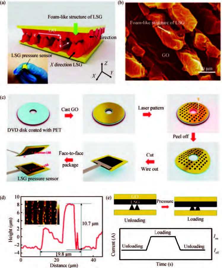
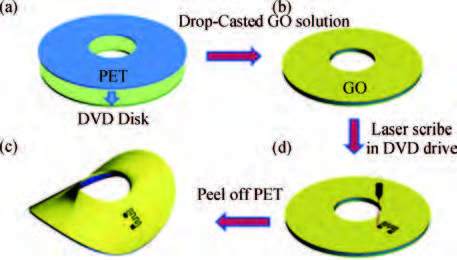
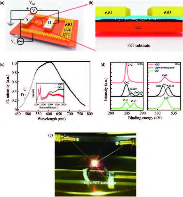
1. Introduction
In the past few years,flexible electronic devices have become a hot topic of scientific research[1, 2, 3],they provide a wide variety of applications including flexible circuits[4],flexible batteries[5],flexible displays[6],and electronic skins[7]. Electronic devices constructed by graphene-based materials have received significant attention.
Graphene,discovered in 2004[8],is an ideal candidate for use in flexible electronic devices due to its fascinating physical properties such as high mobility,excellent thermal and electrical conductivities,high elasticity,a tunable band gap,quantum electronic transport,and high mechanical strength[9]. These superior properties suggest it is quite suitable for novel flexible applications. Although electronic devices constructed from single-layer graphene have such superior characteristics,they are impractical for commercial applications due to the difficulty of fabricating large-scale single-layer graphene[10]. However,graphene-based material provides a practical route for commercialization because of its ease of fabrication via some special technologies. Therefore,some alternative fabrication techniques are required to realize large-scale graphene production and widespread distribution.
Recently,several methods have been developed for large-scale and low-cost graphene production. For example,the technology of chemical vapor deposition (CVD) has been proven efficient for growth and patterning of thin-layer graphene[11],and it has high potential for commercialization. Besides,graphene can also be prepared by reducing solution-based graphene oxide (GO)[12]. Although GO is not conductive,its carbon framework could be restored by thermal treatment,chemical reducing and some other treatments.
In this review,we will discuss the fabrication processes and potential applications of graphene-based flexible electronic devices. In Section 2,we will review some typical fabrication techniques of graphene materials. Besides,some novel techniques based on laser scribing will also be introduced. In Section 3,we emphasize some novel flexible applications based on graphene-based materials including thermal acoustic devices,thermal rectifiers,graphene-based nanogenerators,pressure sensors and graphene-based LEDs. In Section 4,the challenges and outlook of graphene-based flexible electronic devices will be discussed. In Section 5,we will give a brief summary of graphene-based materials and devices.
2. Fabrication techniques of graphene
The characteristics of graphene fabricated in different ways may have big differences. A lot of fabrication techniques are researched so that the fabricated graphene can be suitable in different applications. The fabrication routes of graphene can be broadly categorized into different sections,such as micro-mechanical exfoliation of highly ordered pyrolytic graphite[8, 13, 14],chemical vapor deposition[15, 16, 17, 18, 19, 20, 21, 22, 23, 24, 25, 26],epitaxial growth[27, 28, 29, 30, 31],and the reduction of graphene oxide (GO)[32, 33, 34, 35].
2.1 Exfoliation
Graphite is stacked layers of many graphene sheets,bonded together by inter-layer van der Waals force. Thus,in principle,it is possible to obtain graphene by breaking the van der Waals force between the graphite layers from a high purity graphite sheet. By relying on mechanical or chemical energy to break these inter-layer bonds,an individual graphene sheet is separated out. For a long time,many scientists have tried to separate the two-dimensional crystals which can exist stably in air,however,graphene was first obtained by micromechanical exfoliation from graphite by Andre Geim in 2004[8]. Although this method is a low-budget technique,the samples they obtained are usually at a size of several microns and the thickness is difficult to accurately control,resulting in a low-yield problem. Therefore,the micromechanical exfoliation method is not suitable for large-scale industrial production.
A little different from the original process,Huc etal. have found that large (∼10 μm) and flat graphene flakes can be produced by manipulating the substrate bonding of HOPG on Si substrate and controlled exfoliation[13]. Furthermore,Shukla et al. also created a new method by which mm-sized single-layer to few-layer graphene can be produced by bonding bulk graphite to borosilicate glass followed by exfoliation,to leave single or a few layers of graphene on the substrate[14]. All of these advancements emphasized modifying the bonding with the substrate to generate large-area graphene sheets. With the further optimization and development of these technologies,these approaches show good promise of being used in the industrial-scale production in the near future.
2.2 Chemical vapor deposition techniques
Graphene has also been grown by thermal chemical vapor deposition (T-CVD) from carbon-containing gases on catalytic metal surfaces and/or by surface segregation of carbon dissolved in the bulk of such metals. Carbon sources,such as CH4,C2H2,or solid sources [polystyrene,polyacrylonitrile,polymethyl methacrylate (PMMA) polymers],and various transition metal catalysts (Cu,Ni,Pd,Ru,Ir,or alloys) have been used for graphene growth by T-CVD[15, 16, 17, 18, 19, 20]. Unfortunately,the T-CVD process requires high temperature (>1000℃) in the preparation,so it is not suitable for industrial production. However,plasma-assisted CVD methods can decrease the temperature of the preparation of graphene by combining thermal and plasma energy,which facilitates the decomposition of hydrocarbon at lower temperatures (<1000 ℃)[10, 11, 12].
The electrical properties of CVD-graphene are not convenient to be tested in situ on the conductive metal substrates,therefore it needs to be transferred to a different target substrate after the growth of graphene. Thus,a lot of methods have been developed for the transfer of graphene to an insulating substrate[15, 24]. These methods have been developed for all purposes to reduce defects produced during the transfer process to a suitable target substrate. For the transfer process of graphene,there are mainly two routes. One is the wet-transfer method,using spin-coated PMMA or polydimethylsiloxane (PDMS) as a supporting and protective layer[25]. The other is the dry-transfer method,where we can transfer large-scale graphene onto flexible polymers and rigid substrates[26]. The recent achievements in graphene growth by thermal CVD have confirmed the reproducibility of good quality graphene on a centimeter scale substrate and successful transfer onto many other substrates. However,in the near future,more advanced techniques like the growth of graphene on wafer size substrates,and controlling the number of layers efficiently are urgently-needed.
2.3 Thermal decomposition of silicon carbide
One of the most popular methods for graphene growth is thermal decomposition of Si on the (0001) surface plane of a single crystal of 6H-SiC,which allows for the production of high-quality and large-scale single-layer to multi-layer graphene. In this method,the top layers of SiC crystals undergo thermal decomposition,Si atoms desorb and the carbon atoms remaining on the surface rearrange and re-bond to form epitaxial graphene layers[27, 28]. In most cases,the layers of the graphene grown on this surface are generally between 1 and 3,the number of layers being dependent on the decomposition temperature. In a similar process,Rollings et al. have already obtained graphene films which can be as thin as one-atom thickness[29]. In addition,Emtsev et al. have proposed a new method that in an inert gas atmosphere (e.g.,Ar) at pressures up to 1 bar,the sublimation rate of Si is reduced dramatically,and the thickness of graphene films is limited to only ∼ 1-2 layers[30]. Similar to previous methods,Juang et al. have demonstrated a new synthetic method by which graphene can be synthesized on a Ni thin film coating on the SiC substrate,at a quite lower temperature (750 ℃)[31]. These approaches are promising for large-scale industrial production in the future. Although the process of growing graphene on SiC looks promising,especially for the semiconductor industries,issues like controlling the thickness of the graphene layers and repeated production of large-area graphene have to be solved,before the process can be adopted at an industrial scale.
2.4 Reduction of graphene oxide
The aforementioned fabrication techniques can produce graphene with a relatively perfect structure and excellent properties,while in contrast,GO has two important characteristics: (1) it can be produced using low-cost graphite as a raw material by cost-effective chemical methods with a high yield,and (2) it is highly hydrophilic and can form stable aqueous colloids to facilitate the assembly of macroscopic structures by simple and cheap solution processes,both of which are important to the large-scale use of graphene[33]. Therefore,using the reduction method for graphene fabrication has attracted a lot of attention from researchers.
2.4.1 Solution-based reduction
Solution-based reduction is another route for graphene fabrication. Ruoff's group have demonstrated a solution-based process for obtaining single-layer graphene by chemical exfoliation[32]. The chemical exfoliation method uses strong acids and oxidants to obtain a sheet of GO from graphite powder dispersed in solution. This method usually causes structural and electrical disorder in the graphene during the oxidation process,so it is necessary to add an additional process to enhance the electrical property of GO due to the oxygen-rich functional groups on the GO's surface. Although this method is a simple and solution-based process and can produce large quantities of graphene at low cost,the electrical and optical properties of rGO films are inferior to those of the graphene films produced by mechanical exfoliation or CVD methods.
2.4.2 Thermal reduction
Yang $et al.$. have demonstrated that graphene oxide thin films can be reduced by heat treatment in an ultra-high vacuum or a reducing atmosphere at high temperatures of 900-1000 ℃[34]. The mechanism of this method is mainly the sudden expansion of CO or CO2 gases between graphene sheets during rapid heating of the graphite oxide. The rapid temperature increase makes the oxygen-containing functional groups attached on the carbon plane decompose into gases,which then creates huge pressure between the stacked layers. However,this technique can only be used to produce small size and wrinkled graphene sheets.
2.4.3 Laser-scribing reduction
Thermal reduction is usually carried out by thermal irradiation. As an alternative,some novel heating resources have been tried to realize thermal reduction such as laser irradiation and so forth. A new technique named laser-scribing reduction has been proposed by Zhang et al. by which patterned film fabrication is carried out with femtosecond laser irradiation[35]. As a result,the laser reduction can produce rGO films with a much higher conductivity.
Applications of graphene-based flexible electronic devices
3.1 Graphene-based thermal acoustic devices
The working principle of traditional acoustic devices is based on mechanical vibration,the sound pressure performs well in the low frequency domain,however the performance becomes poor when the frequency rises[36]. Compared with traditional devices,some acoustic devices based on the thermal acoustic effect perform excellently in the high frequency domain[36, 37, 38]. Graphene has a very high thermal conductivity[39] and low heat capacity per unit area[40],so it is possible to fabricate an efficient sound-emitting device based on its excellent characteristics[41]. The principle is based on the thermal acoustic effect,so no mechanical vibration is needed[42]. Many metal films and nano materials thin films have been reported to work as sound-emitting devices (SEDs)[43, 44, 45, 46, 47]. Recently single-layer graphene (SLG) was demonstrated to work as a sound emitting device by He Tian et al.[37] SLG has the thinnest layer in all materials. It has an electrical mobility of 2 × 105 cm2/(V⋅s) at room temperature[48]. Moreover,its thermal conductivity is ∼5000 W/(m⋅K)[49]. Because of the low heat capacity per unit area,SLG could be used as an excellent sound emitting material[50].
He Tian et al.. fabricated a wafer-scale flexible graphene-based loudspeaker by a simple process and studied the acoustic characteristics of the graphene[51]. A DVD burner with a laser scribe function has been chosen. The wavelength of the laser is 788 nm and the power is 5 mW. The stack single-layer graphene oxide (GO) film is changed into graphene (Figure1). In order to realize a flexible device,a PET substrate is used. The fabrication process could be described as follows. Firstly,the PET is covered on the DVD disc. Secondly,a GO solution is coated onto the PET. After the GO is dry,the disk is put into the DVD burner to write graphene patterns. Lastly,the PET is peeled off from the DVD disc and the graphene loudspeakers are done. In order to realize the predesigned structure,a PC software is used to import a designed patterning. The software could control the DVD drive to reduce GO into graphene selectively.

When a sound signal is applied to graphene,the air near its surface will be heated up by the Joule heating,then the air's periodicity vibration will form sound waves shown in Figure2(a). The I-V curve of graphene after laser scribing is shown in Figure2(b). The Raman spectrum obtained from the graphene film is shown in Figure2(c). The graphene film exhibits typical monolayer graphene features with a sharp G peak and a single 2D peak. The sound pressure of the device is shown in Figure2(d).

The sound emission from graphene was different because of the power,distance,directivity and frequency[52]. Graphene can produce a broader frequency than other materials. The sound emission from graphene had a good performance ranging from 20 to 50 kHz. The device could be integrated into LCDs to form multifunctional systems.
3.2 Graphene-based thermal rectifiers
Since silicon technology always develops under Moore's laws,the feature size has a bottleneck below 10 nm. Graphene is predicted to replace silicon[53] as the next generation material,because of the outstanding electrical[54],mechanical[55],thermal[56],and optical properties[57].The integrated circuits can be made of diodes and transistors with the development of solid-state devices[58]. If we can control the thermal conduction,we can also realize thermal circuits by using these phononics devices[59]. In addition to information processing,the thermal devices must have many applications for heat control in the future[60]. Recently,many researchers have put forward some theoretical proposals for the thermal rectifier including structures based on one-dimensional nanotubes and nanowires,and two-dimensional graphene[61, 62, 63]. Gordiz et al. observed thermal rectification in multi-walled carbon nanotubes[64]. Thermal devices have gradually converted from fundamental science to applied research field[65].
Recently Tian et al. demonstrated the thermal rectification phenomenon in asymmetric reduced graphene oxide (rGO) materials[66]. It has been demonstrated theoretically,and a larger rectification ratio can be achieved in multi-layer graphene structures. Combined with the availability of high quality,here an “rGO paper” material is used composed of stacked rGO to make a thermal rectifier. Because of the high thermal conductivity,a high thermal rectification ratio is achieved in a triangular and two-rectangular shaped rGO based thermal rectifier.
Figure3(a) shows the optical photograph of the rGO paper and Figure3(b) illustrates the surface of the rGO film. The cross-section of the rGO is shown in Figure3(c). The film thickness of the rGO is ∼50 mm. Figure3(d) presents the energy dispersive X-ray (EDX) spectrum of the rGO film. Meanwhile,the rectification coefficient in the rGO is much higher than that in a carbon nanotube. The heat power versus the angle of the rGO paper is shown in Figure3(e). From Figure3(f) we can see that the rectification coefficient increases linearly with the angle of the rGO paper.

The triangular and two-rectangular shaped rGO thermal rectifier experimentally is analyzed. The two-rectangular shaped sample has the rectification coefficient of 1.10. The results shed light on the macroscopic phononic device with graphene.
3.3 Graphene-based nanogenerators
Now oil,natural gas and coal's reserves are limited. The harvesting of energy from the environment is an effective way to actuate nanodevices. A series of nanogenerators based on nano materials are fabricated[68, 69, 70, 71, 72, 73]. Que et al. developed a flexible nanogenerator with an energy conversion efficiency of 12.1%[74]. Besides,He Tian et al.. demonstrated a flexible nanogenerator based on GO film[75]. A multi-layer structure with Al/PI/GO/PI/ITO is made on the PET substrate. A peak voltage of 2 V and a current of 30 nA can be generated by the GO nanogenerator upon the repetitive application of a 15 N force with a frequency of 1 Hz. Moreover,the output voltage can increase to 34.4 V by the frequency of 10 Hz.
A schematic view of the flexible GO-based nanogenerator (GONG) is shown in Figure4(a) and photographs of the GONG under bending are shown in Figure4(b),and also of the front side and the back side. The fabrication process is shown in Figure4(c). The GO film was then fixed onto this PI tape layer. The area of the PET plate was about 3 × 3 cm2 and the thickness was about 0.7 mm,respectively. Then we can apply another layer of PI tape above the GO film. Finally,the Al membrane was installed above the film. A photograph of the GO film under bending is shown in Figure4(d),demonstrating its good flexibility. A cross section image of the GO film under SEM is shown in Figure4(e). The thickness of the GO film is ∼20 mm. The surface profile of a GO film with an area of 1 × 1 cm2 is shown in Figure4(f). The surface profile of a GO film under SEM is shown in Figure4(g),in which the ripples of the graphene oxide are clearly visible. %A peak voltage of 2 V and a current of 30 nA can be generated by the GO nanogenerator upon the repetitive application of a 15 N force with a frequency of 1 Hz. Moreover,the output voltage can increase to 34.4 V by the frequency of 10 Hz.

The graphene-based nanogenerator will be applied to power an LCD,LED and other electrical components without any other external energy source. The flexible nanogenerator will be suitable for all-parts of flexible electronic devices. It will provide a simple method for harvesting mechanical energy by flexible graphene-based materials and power low-power portable devices,and it can be the basis of self-powered electronic systems.
3.4 Graphene-based pressure and strain sensors
Pressure sensors are very important in electronic skin (e-skin) sensing systems[76, 77, 78, 79, 80, 81, 82]. One of the most useful applications of graphene-based materials is their uses as pressure and strain sensors[83, 84, 85]. Most usually,the pressure and strain cause the change of resistance of graphene-based materials. We can get the intensity of pressure and strain by monitoring the change of resistance. Resistive pressure sensors usually have a high sensitivity when the pressure is very low (<5 kPa) so as to enable ultra-sensitive detection. However,the sensitivity performs badly at high pressures (>5 kPa),which cannot adapt to practical applications[86, 87, 88]. A gentle touch and object manipulation acts with pressures below 10 kPa,and 10-100 kPa,respectively[89]. There is a desire to maintaining a high sensitivity in a wide pressure range[90]. Tian,Shu,and Wang et al. demonstrated a pressure sensor with a foam-like structure based on laser-scribed graphene (LSG) which is flexible,wide range and ultra-sensitive resistive[79]. The sensitivity of the pressure sensor is 0.96 kPa−1 with a wide pressure range (0-50 kPa) because of the large spacing between graphene layers and the v-shaped microstructure of the LSG. The pressure sensor performs better than all reported pressure sensors to date when it comes to both sensitivity and the pressure sensing range.
Figure5(a) shows the device structure of the LSG pressure sensor[79]. The most important component of pressure sensing is a crossbar structure. Figure5(b) shows the structure contains a face-to-face stack of two LSG films patterned as v-shaped gratings. Figure5(c) shows the process of the fabrication of the LSG pressure sensor. The LSG film patterning is based on the reduction of graphene oxide (GO) using the DVD laser-scribing function. Different from the dense GO films,the LSG consists of loosely stacked graphene layers. Figure5(d) shows that the height and width of the LSG is 10.7 and 19.8 μm with a v-shape result from the height profile. Figure5(e) shows the sensing mechanism and current changes in response to loading and unloading.

In addition,graphene-based strain sensors also have an enormous potential application value in the wearable electronics field[84, 91]. Attributed to its piezoresistive effect,Zhao et al. developed novel nanographene strain sensors with gauge factors over 300[92]. Hempel et al. invented a high performance strain sensor by a spraying solution[93]. What is more,Li et al. improved the stretch performance by choosing graphene woven fabrics[94]. Compared with traditional metal strain sensors,the graphene-based strain sensors have a much better performance. However,the growth and patterning of graphene-based strain sensors remain a challenging issue. Tian et al. developed a one-step laser scribing technology to fabricate large-scale graphene strain sensors[95].
Figure6 shows schematic diagrams of the fabrication process for flexible graphene-on-PET strain sensors[95]. The fabrication process could be described as follows. Firstly,a PET film is coated on a DVD disc (Figure6(a)). Then,the GO solution is drop-cast on the DVD disc (Figure6(b)). After the GO layer is dried,the disc is inserted into a light-scribe DVD drive and a computer-designed circuit is etched onto the film. The laser inside the drive converts the golden-brown GO into black graphene at precise locations to produce graphene strain sensors. With the laser scribing technology,large areas of precise graphene patterns completed in ∼25 min are achieved (Figure6(c)). Finally,wafer-scale flexible graphene-on-PET strain sensors could be obtained by peeling off the substrate from the disc (Figure6(d)).

3.5 Graphene-based light-emitting diode (LED)
The solid-state light-emitting diode (LED) is a very important electronic device in daily life. The invention of LEDs has improved high-performance displays[96, 97]. With the development of flexible displays,flexible light emitting devices are a challenging task. Traditional LEDS are fabricated in predesigned colors whose wavelength is determined by designing the materials and structures. Graphene-based materials are used as photonic devices by many scholars[98, 99, 100, 101, 102],however the development of graphene-based LEDs comes across many difficulties due to its vanishing bandgap.
Kim et al. developed a bright visible light emitting device based on freely suspended graphene fabricated by the CVD method[103]. However the graphene grows on the silicon substrate in this device,so it is not a totally flexible device. He Tian etal. combined a bandgap structure and a bipolar carrier injection in a special type of semi-reduced graphene oxide (GO),and developed a spectrally tunable graphene-based flexible field-effect light-emitting device[104].
Figure7 describes the structure of the spectrally tunable graphene-based flexible LED[104]. The planar side gate is prepared by laser-scribing technology. The light-emitting layer is the interface between the GO and rGO. The typical length of the emitting region is 80-120 μm.

4. Challenges and outlook
There are still a lot of challenges we need to solve,although the advantages of graphene-based materials are obvious. Firstly,graphene-based materials are quite fragile and easily broken during practical application. Combining graphene-based materials with elastic polymers is a new way to improve the stability,and surface modification or optimization of crosslinking agents are some novel methods to expanding their applications. These problems will continue to be focused on until we develop some new techniques to improve their inter-layer binding so that they could be more robust. In view of the scale,the fabrication techniques of large-scale graphene-based materials are still not mature. Expanding the volume of the furnace which can contain larger sheet graphene and promoting the uniformity of graphene may be some attempted methods to overcome these challenges. Besides,the laser scribing technique should be optimized in the future,because it is a promising technique to realize large-scale and low-cost graphene production.
The challenges of graphene-based materials will require continued innovative study and research. It is not clear the graphene-based materials described here will dominate the flexible electronic devices market,but it undoubtedly will continue to increase. A huge number of novel materials,such as metallic nanoparticles,metallic nanowires,inorganic nanowires,organic polymers and so on,are in direct competition with graphene-based materials in the area of flexible electronic devices. Although some of them are stretchable and flexible,the mobility or conductivity is not ideal at the same time. Besides the lifetime and stability of other novel materials are also constrained. However,they also have some advantages over graphene-based materials in some specific area,so we need to accelerate the speed of solving these issues described above.
According to the report of IDTechEx,a consulting company,the market share for flexible and printed electronics will be $63.28 billion by 2022. Most likely,the most commercial need of graphene-based materials in flexible electronic devices will be transparent and flexible source and wearable electronics. In the next step,more complicated systems such as flexible logic circuits and memory could also be realized by graphene-based materials
5. Conclusions
In conclusion,with their high surface area,high stability,high mobility,high electro/thermo conductivities,high elasticity and high flexibility graphene-based materials have been used in different kinds of flexible electronic devices successfully. This paper reports the recent progress in the fabrication techniques and applications of graphene-based materials to give a guide for its future improvement and development.