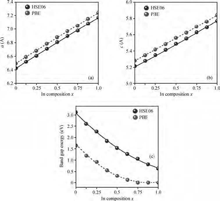
Processing math: 100%
J. Semicond. > 2016, Volume 37 > Issue 4 > 042001

SEMICONDUCTOR PHYSICS

Hybrid functional calculations on the band gap bowing parameters of InxGa1-xN

Mei Lin1, Yixu Xu1, Jianhua Zhang2, Shunqing Wu1 and Zizhong Zhu1, 3,

+ Author Affiliations

 Corresponding author: Zizhong Zhu, Email:zzhu@xmu.edu.cn

DOI: 10.1088/1674-4926/37/4/042001

PDF

Abstract: The electronic band structures and band gap bowing parameters of InxGa1-xN are studied by the first-principles method based on the density functional theory. Calculations by employing both the Heyd-Scuseria-Ernzerh of hybrid functional (HSE06) and the Perdew-Burke-Ernzerhof (PBE) one are performed. We found that the theoretical band gap bowing parameter is dependent significantly on the calculation method, especially on the exchange-correlation functional employed in the DFT calculations. The band gap of InxGa1-xN alloy decreases considerably when the In constituent x increases. It is the interactions of s-s and p-p orbitals between anions and cations that play significant roles in formatting the band gaps bowing. In general, the HSE06 hybrid functional could provide a good alternative to the PBE functional in calculating the band gap bowing parameters.

Key words: InxGa1-xNbowing parametersHSE06 functionalPBE functional

In recent years,the InxGa1xN alloy has been studied extensively[1, 2, 3]. The special character of this alloy is that the energy gap can be varied in a wide spectral range,since it is capable of being tuned from the visible across the ultraviolet spectral range[4]. In the past decade,remarkable progress has been made in the development of electronic and optical devices based on the InxGa1xN alloys. For example,electronic devices such as light emitting diodes and laser diodes operating in the green-blue-UV spectral region have been successfully fabricated by the use of the ternary InxGa1xN alloys[5].

The successful electronic and optical applications of the InxGa1xN system are based on the superior band structures of InxGa1xN,for example,alloying among the group-III nitrides allows a change in the band gap from 1.89 eV in InN (some reported a much lower value[6] to 6.28 eV in AlN with an intermediate value of 3.44 eV for GaN at 300 K[1]. Such a wide spectral range gives possibilities for the use of (InGaAl)N in a variety of device applications. The energy gaps of the InxGa1xN alloy provide an almost perfect match with the complete solar spectrum,which makes InxGa1xN a potential material for highly efficient solar cells. In the past,a number of theoretical[7, 8, 9, 10, 11, 12] and experimental[13, 14, 15, 16] studies have investigated the band gap as a function of x composition.

However,no agreement has been reached on the magnitude of the band gap bowing parameter,e.g.,a 1.44 eV[9] was found by first-principles total energy calculations with the generalized quasichemical approach,a 1.36 eV[10] was reached by the first-principles HSE06 functional calculations and a 1.513 eV[11] was obtained from the linear muffin-tin orbital density functional theory method with the semilocal modified Becke-Johnson exchange potential. Even,there are still disagreements on the issue of whether a single bowing parameter can describe the gap over the entire range of composition x. Therefore,a detailed study on the band structures of InxGa1xN is still essential for understanding the optoelectronic properties of InxGa1xN alloys.

It is well known that the calculated band gaps by employing the local-density approximation (LDA)[17] and even the Perdew-Burke-Ernzerhof (PBE) functional[18] for III-nitrides are significantly smaller than the experimental ones due to the intrinsic errors in describing the excited states of the methods. An advanced method such as GW[19] improves this aspect but it requires an additional computational effort that is considerable. Therefore,in the present work,we take advantage of the more efficient hybrid functional,i.e.,the Heyd-Scuseria-Ernzerhof hybrid functional (HSE06)[20, 21, 22],for describing the exchange and correlation functional in the DFT to overcome the band-gap problem. This allows accurate calculations of the band gaps and the alignment of energy bands in InxGa1xN alloys.

The present calculations have been performed by using the Vienna ab initio simulation package (VASP),which is based on the density functional theory,the plane-wave basis and the projector augmented wave (PAW) representation[23]. The generalized gradient approximation (GGA) in both the forms of Perdew-Burke-Ernzerhof (PBE) functional[18] and the Heyd-Scuseria-Ernzerhof hybrid functional (HSE06)[22] are used to treat the exchange-correlation energy. Wave functions are expanded by plane waves up to a kinetic energy cutoff of 500 eV. Brillouin-zone integrations are approximated by using special k-points sampling of the Monkhorst-Pack scheme[24] with a 9 × 9 × 11 grid in the PBE and a 5 × 5 × 7 grid in the HSE06 methods. The Ga 3d and In 4d electrons are treated as valence electrons in both the PBE and HSE06 methods.

The hybrid treatment on the exchange and correlation energy by the HSE06 method has proved to obtain more accurate band structures than the PBE method. In HSE06,the exchange-correlation energy is defined as follows:

EHSE06xc=14EHF,SRx(ω)+34EPBE,SRx(ω)+EPBE,LRx(ω)+EPBEc,

(1)

where EHF,SRx(ω),EPBE,SRx(ω),EPBE,LRx(ω) and EPBEc represent the short-range (SR) Hartree-Fock (HF) exchange,the short-range PBE exchange,the long-range (LR) PBE exchange and the PBE correlation terms,respectively. The HSE06 functional partitions the Coulomb potential for exchange into short-range and long-range components by

1r=1erf(ωr)r+erf(ωr)r,

(2)

where ω is an adjustable parameter. For ω=0,the long-range term becomes zero and the short-range term is equivalent to the full Coulomb operator. The opposite is the case for ω. The screening parameter ω is related to a characteristic distance,2/ω,at which the short-range interactions become negligible. Empirically,it was shown that the optimum range-separation parameter ω is between 0.2 and 0.3[22]. In this work,the parameter ω is set to be 0.2 Å1.

For the study of geometrical and electronic structures of wurtzite InxGa1xN,a 16-atoms supercell of InxGa1xN has been adopted in the present calculations,which corresponds to a 2 × 2 × 1 the size of the primitive cell of GaN or InN. Here,we choose to calculate only the In composition of x = 0,1/8,2/8,,7/8 and 1.0. For a given number of x of InxGa1xN,the atomic configurations and the sizes of supercells are fully relaxed. For x = 0 and 1.0,the bulk GaN and InN are calculated. For x = 1/8,there are eight possible substitution sites for the In atoms. We have calculated all the eight structures and the structure with the minimum energy is recorded and analyzed. For x = 7/8,there are eight possible sites for the Ga atoms,which are not replaced by In. All the eight structures have been optimized and analyzed. For the calculations of x = 2/8,3/8,4/8,an approximation has been made. For example,for x = 2/8,only seven possible structures (seven possible sites left for the second In atom besides the first substitution In) based on x = 1/8 are studied. The same approximation is applied to x = 3/8,4/8. That is,only six (five) possible sites are left for the third (fourth) In atoms at x = 3/8 (4/8) based on the structures of x = 2/8 (3/8). Only these structures are calculated. The same approximation is also applied to x = 6/8,5/8. There are seven (six) possible sites for the second (third) Ga atoms in InxGa1xN at x = 6/8 (5/8) relative to x = 7/8 (6/8); all these structures are calculated as above.

The lattice constants a and c as a function of the In composition x are shown in Figures 1(a) and 1(b). It shows that the lattice constants a and c increase with the increasing of In composition x. The reason for this should be due to the atomic size of In which is larger than that of Ga. The increasing of a and c is quite linear as a function of In composition x. The lattice constants calculated from the PBE method are always larger than those from the HSE06 method. The curves shown in Figures 1(a) and 1(b) can be approximately fitted by using the following formulas,respectively,

{a(x)=xaInN+(1x)aGaNδax(1x),c(x)=xcInN+(1x)cGaNδcx(1x),

(3)

where a(x) and c(x) are lattice constants of InxGa1xN,while δa and δc are the deviation parameters for lattice constants a and c. The results give δa=0.026±0.0095 Å and δc=0.049±0.0357 Å. The δa and δc here are both small,which indicates that our results are close to those from Vegard's law[25].

The band gaps calculated by both the PBE and HSE06 methods for the optimized structures as described above are listed in Table1 and shown in Figure1(c),as a function of In concentration x in InxGa1xN. It is well known that energy gaps are systematically underestimated by local density approximation (LDA) and generalized gradient approximation (GGA). On the other hand,however,a hybrid functional method,such as HSE06 functional,has been shown to give much better band gap values in a variety of semiconductors. In order to see the functional dependence of the band gap values in the entire composition range for the InxGa1xN alloy system,two sets of data,i.e. by using the PBE method and the HSE06 functional method to describe the exchange-correlation functionals in DFT,are shown in Figure1. As expected,band gaps calculated from the PBE method are much smaller than those of experimental values. On the other hand,band gap results from the hybrid functional show a much better agreement with experimental data (for GaN and InN bulk,in Table1). The band gaps as shown in Figure1(c) can be depicted by the following formula,as a function of In composition x:

Eg(x)=xEgInN+(1x)EgGaNbx(1x).

(4)
Table  1.  Energy gaps and bowing parameters of InxGa1xN system calculated by PBE and HSE06 functional methods,compared with available theoretical and experimental data.
DownLoad: CSV  | Show Table
Figure  1.  (a) Lattice constants a as a function of the In composition x. (b) Lattice constants c as a function of the In content x. (c) Band gap as a function of the In composition x.

The deviation from the linear behavior of Eg-x is usually characterized by the bowing parameter b in the above equation. The band gap bowing parameters are shown to be 2.202 eV (by PBE) and 1.311 eV (by HSE06) in the present calculations. Apparently,the bowing parameter from the HSE06 calculation is clearly smaller than that from the PBE calculation. The hybrid functional result is in good agreement with the experimentally measured value of 1.43 eV for wurtzite InxGa1xN[6] and also in close proximity to the theoretically calculated value of 1.36 eV[10]. Overall,the present HSE06 hybrid functional could provide a good alternative to the PBE functional in calculating the band gap bowing parameters.

In order to understand the electronic structures of InxGa1xN alloys,the total and atomic orbital decomposed partial density of states (TDOS and PDOS) of GaN are compared with those of InN and the PDOS of InxGa1xN,and shown in Figure2. The contributions of s- and p-orbitals of anions and cations are also presented in Figure3. All the results are calculated by the HSE06 method for the wurtize structure. Although the profiles of the TDOS curves of GaN and InN are quite similar,the atomic orbital contributions to the TDOS are somewhat different (see PDOS in Figure2(a)). For example,the electronic states around the valence band maximum (VBM) of GaN is mainly contributed by the N-p and Ga-p electrons interactions (p-p interactions) and somewhat the coupling of p-d orbitals,however,electronic states around VBM of InN are contributed not only by the N-p and In-p electron interactions,but also by the N-s and In-s electron interactions (s-s interactions),as well as some involvement of the In-d orbital. For the electronic states around the conduction band minimum (CBM),it can be seen from Figure3 that the anion-s (N-s) and cation-s (Ga-s or In-s) components have the largest contributions to the electronic states. The band gap of GaN and InN is then mainly determined by the anion and cation p-p interactions relative to the s-s interactions.

Figure  2.  (Color online) (a) Total and partial density of states (TDOS and PDOS) of bulk GaN,compared with those of bulk InN. (b) Partial density of states (PDOS) of InxGa1xN alloys,calculated by the HSE06 method.
Figure  3.  (Color online) (a) Contributions of s-orbitals of anions and cations to the band structures of InxGa1xN. (b) Contributions of p-orbitals of anions and cations to the band structures of InxGa1xN. The results are calculated by the HSE06 method. Black curves are mainly the valence bands.

For the InxGa1xN alloys,the band gap is shown to decrease as the In concentration x increases. This trend can be explained as follows. The conduction band edge derives mainly from the unoccupied states of anion and cation s-orbitals (see Figure3) and the coupling of anion-p and cation-d electrons (as shown in Figure2). The down movement of the CBM originates from the decrease of s-s repulsion when x concentration increases,due to the In-N bond length being larger than that of Ga-N. By investigating the atomic orbital contributions to the band structures under different constituents of the alloy,we see that the anion-s contribution is weakened while the cation-s contribution is strengthened around the CBM when In composition x increases (shown in Figure3(a)). Besides,the valence band edge stems mainly from the anion-p and cation-p bonding states as well as a small part of couplings of the anion-p and cation-d states. The bond length of In-N is larger than that of Ga-N,which should reduce the p-p coupling[26] when In concentration x increases and results in higher bonding VBM energies. On the other hand,another factor determining the valence band edge is the interaction between the cation-d and anion-p if p-d couplings in these systems are taken into account. The energies of the Ga-3d and the In-4d orbital are below the anion-p energy,so p-d repulsion pushes the anion-p VBM up in energy. In short,the anion and cation s-s and p-p electron interactions play a main effect in determining the band gap bowing[27],while p-d repulsion has also an effect in influencing the formation of VBM.

Band gap values and bowing parameters of InxGa1xN have been studied by the well-established first-principles method,based on the density functional theory and the PBE functional and HSE06 hybrid functional. The HSE06 functional has been shown to be more rational than the PBE one in predicting the band gaps and band gap bowing parameter. The bowing parameter,1.311 eV,from our HSE06 method calculation is in good agreement with the experimentally measured value of 1.43 eV and also in close proximity to the theoretically calculated value of 1.36 eV. The anion and cation s-s and p-p electron interactions play a main effect in formatting the band gap bowing,whose CBM is weakened as the In constituent increases. Meanwhile,the p-d repulsion also has an effect in influencing the formation of VBM.


[1]
[2]
[3]
[4]
[5]
[6]
[7]
[8]
[9]
[10]
[11]
[12]
[13]
[14]
[15]
[16]
[17]
[18]
[19]
[20]
[21]
[22]
[23]
[24]
[25]
[26]
[27]
Fig. 1.  (a) Lattice constants a as a function of the In composition x. (b) Lattice constants c as a function of the In content x. (c) Band gap as a function of the In composition x.

Fig. 2.  (Color online) (a) Total and partial density of states (TDOS and PDOS) of bulk GaN,compared with those of bulk InN. (b) Partial density of states (PDOS) of InxGa1xN alloys,calculated by the HSE06 method.

Fig. 3.  (Color online) (a) Contributions of s-orbitals of anions and cations to the band structures of InxGa1xN. (b) Contributions of p-orbitals of anions and cations to the band structures of InxGa1xN. The results are calculated by the HSE06 method. Black curves are mainly the valence bands.

Table 1.   Energy gaps and bowing parameters of InxGa1xN system calculated by PBE and HSE06 functional methods,compared with available theoretical and experimental data.

DownLoad: CSV
[1]
[2]
[3]
[4]
[5]
[6]
[7]
[8]
[9]
[10]
[11]
[12]
[13]
[14]
[15]
[16]
[17]
[18]
[19]
[20]
[21]
[22]
[23]
[24]
[25]
[26]
[27]
1

Analytical model for the effects of the variation of ferrolectric material parameters on the minimum subthreshold swing in negative capacitance capacitor

Raheela Rasool, Najeeb-ud-Din, G. M. Rather

Journal of Semiconductors, 2019, 40(12): 122401. doi: 10.1088/1674-4926/40/12/122401

2

Hybrid functional microfibers for textile electronics and biosensors

Bichitra Nanda Sahoo, Byungwoo Choi, Jungmok Seo, Taeyoon Lee

Journal of Semiconductors, 2018, 39(1): 011009. doi: 10.1088/1674-4926/39/1/011009

3

Schottky barrier parameters and structural properties of rapidly annealed Zr Schottky electrode on p-type GaN

V. Rajagopal Reddy, B. Asha, Chel-Jong Choi

Journal of Semiconductors, 2017, 38(6): 064001. doi: 10.1088/1674-4926/38/6/064001

4

Modeling the drain current and its equation parameters for lightly doped symmetrical double-gate MOSFETs

Mini Bhartia, Arun Kumar Chatterjee

Journal of Semiconductors, 2015, 36(4): 044003. doi: 10.1088/1674-4926/36/4/044003

5

Structural parameters improvement of an integrated HBT in a cascode configuration opto-electronic mixer

Hassan Kaatuzian, Hadi Dehghan Nayeri, Masoud Ataei, Ashkan Zandi

Journal of Semiconductors, 2013, 34(9): 094001. doi: 10.1088/1674-4926/34/9/094001

6

Parameters influencing the optical properties of SnS thin films

Priyal Jain, P. Arun

Journal of Semiconductors, 2013, 34(9): 093004. doi: 10.1088/1674-4926/34/9/093004

7

Bound polaron in a strained wurtzite GaN/AlxGa1-xN cylindrical quantum dot

Zhang Bin, Yan Zuwei, Zhang Min

Journal of Semiconductors, 2011, 32(6): 062003. doi: 10.1088/1674-4926/32/6/062003

8

X-ray reflectivity and atomic force microscopy studies of MOCVD grown AlxGa1-xN/GaN superlattice structures

Wang Yuanzhang, Li Jinchai, Li Shuping, Chen Hangyang, Liu Dayi, et al.

Journal of Semiconductors, 2011, 32(4): 043006. doi: 10.1088/1674-4926/32/4/043006

9

Simulation of electrical properties of InxAl1-xN/AlN/GaN high electron mobility transistor structure

Bi Yang, Wang Xiaoliang, Xiao Hongling, Wang Cuimei, Yang Cuibai, et al.

Journal of Semiconductors, 2011, 32(8): 083003. doi: 10.1088/1674-4926/32/8/083003

10

Binding energies of shallow impurities in asymmetric strained wurtzite AlxGa1-xN/GaN/AlyGa1-yN quantum wells

Ha Sihua, Ban Shiliang, Zhu Jun

Journal of Semiconductors, 2011, 32(4): 042001. doi: 10.1088/1674-4926/32/4/042001

11

Pressure influence on bound polarons in a strained wurtzite GaN/AlxGa1-xN heterojunction under an electric field

Zhang Min, Ban Shiliang

Journal of Semiconductors, 2010, 31(5): 052002. doi: 10.1088/1674-4926/31/5/052002

12

Effects of the reciprocating parameters of the carrier on material removal rate and non-uniformity in CMP

Wang Cailing, Kang Renke, Jin Zhuji, Guo Dongming

Journal of Semiconductors, 2010, 31(12): 126001. doi: 10.1088/1674-4926/31/12/126001

13

Monolithic white LED based on AlxGa1-xN/InyGa1-yN DBR resonant-cavity

Chen Yu, Huang Lirong, Zhu Shanshan

Journal of Semiconductors, 2009, 30(1): 014005. doi: 10.1088/1674-4926/30/1/014005

14

Small-signal model parameter extraction for microwave SiGe HBTs based on Y- and Z-parameter characterization

Fu Jun

Journal of Semiconductors, 2009, 30(8): 084005. doi: 10.1088/1674-4926/30/8/084005

15

High-temperature characteristics of AlxGa1–xN/GaN Schottky diodes

Zhang Xiaoling, Li Fei, Lu Changzhi, Xie Xuesong, Li Ying, et al.

Journal of Semiconductors, 2009, 30(3): 034001. doi: 10.1088/1674-4926/30/3/034001

16

High Temperature Performance of GaN and AIxGal-xN/GaN Heterostructures

Wang Maojun, Shen Bo, Wang Yan, Huang Sen, Xu Fujun, et al.

Chinese Journal of Semiconductors , 2007, 28(S1): 376-378.

17

Elastic-Plastic Mechanical Properties of AlxGa1-xN Thin Films with High Al Composition

Xu Fujun, Shen Bo, Wang Maojun, Xu jian, Miao Zhenlin, et al.

Chinese Journal of Semiconductors , 2007, 28(10): 1551-1554.

18

Stillinger-Weber Parameters for InN:Application to InxGa1-xN

Lei Huaping, Jiang Xunya, Yu Guanghui, Chen J, Petit S, et al.

Chinese Journal of Semiconductors , 2007, 28(S1): 12-15.

19

Influence of Polarization-Induced Electric Fields on Optical Properties of Intersubband Transitions in AlxGa1-xN/GaN Double Quantum Wells

Lei Shuangying, Shen Bo, Xu Fujun, Yang Zhijian, Xu Ke, et al.

Chinese Journal of Semiconductors , 2006, 27(3): 403-408.

20

Investigation of Indium Surface Segregation in InxGa1-xN Films

Liu Chengxiang, Xie Zili, Han Ping, Liu Bin, Li Liang, et al.

Chinese Journal of Semiconductors , 2006, 27(S1): 97-100.

  • Search

    Advanced Search >>

    GET CITATION

    Mei Lin, Yixu Xu, Jianhua Zhang, Shunqing Wu, Zizhong Zhu. Hybrid functional calculations on the band gap bowing parameters of InxGa1-xN[J]. Journal of Semiconductors, 2016, 37(4): 042001. doi: 10.1088/1674-4926/37/4/042001
    M Lin, Y X Xu, J H Zhang, S Q Wu, Z Z Zhu. Hybrid functional calculations on the band gap bowing parameters of InxGa1-xN[J]. J. Semicond., 2016, 37(4): 042001. doi: 10.1088/1674-4926/37/4/042001.
    shu

    Export: BibTex EndNote

    Article Metrics

    Article views: 2519 Times PDF downloads: 19 Times Cited by: 0 Times

    History

    Received: 04 August 2015 Revised: Online: Published: 01 April 2016

    Catalog

      Email This Article

      User name:
      Email:*请输入正确邮箱
      Code:*验证码错误
      Mei Lin, Yixu Xu, Jianhua Zhang, Shunqing Wu, Zizhong Zhu. Hybrid functional calculations on the band gap bowing parameters of InxGa1-xN[J]. Journal of Semiconductors, 2016, 37(4): 042001. doi: 10.1088/1674-4926/37/4/042001 ****M Lin, Y X Xu, J H Zhang, S Q Wu, Z Z Zhu. Hybrid functional calculations on the band gap bowing parameters of InxGa1-xN[J]. J. Semicond., 2016, 37(4): 042001. doi: 10.1088/1674-4926/37/4/042001.
      Citation:
      Mei Lin, Yixu Xu, Jianhua Zhang, Shunqing Wu, Zizhong Zhu. Hybrid functional calculations on the band gap bowing parameters of InxGa1-xN[J]. Journal of Semiconductors, 2016, 37(4): 042001. doi: 10.1088/1674-4926/37/4/042001 ****
      M Lin, Y X Xu, J H Zhang, S Q Wu, Z Z Zhu. Hybrid functional calculations on the band gap bowing parameters of InxGa1-xN[J]. J. Semicond., 2016, 37(4): 042001. doi: 10.1088/1674-4926/37/4/042001.

      Hybrid functional calculations on the band gap bowing parameters of InxGa1-xN

      DOI: 10.1088/1674-4926/37/4/042001
      Funds:

      Project supported by the National Natural Science Foundation of China (Nos. 11204257, 21233004) and the China Postdoctoral Science Foundation (No. 2012M511447).

      More Information
      • Corresponding author: Email:zzhu@xmu.edu.cn
      • Received Date: 2015-08-04
      • Accepted Date: 2015-09-07
      • Published Date: 2016-01-25

      Catalog

        /

        DownLoad:  Full-Size Img  PowerPoint
        Return
        Return