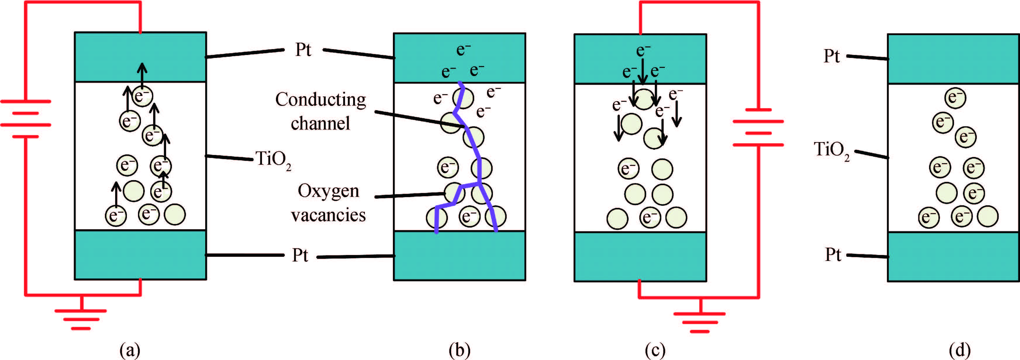
Fig. 1.
Typical construction of memristive devices.
(a) Titanium oxide memristive device with TiO2 bulk layer. (b) Tantalum oxide memristive device with TaO2 bulk layer and Ta2O5 insulator layer.
SEMICONDUCTOR DEVICES
Patrick W. C. Ho, Firas Odai Hatem, Haider Abbas F. Almurib and T. Nandha Kumar
Corresponding author: Patrick W. C. Ho Email: kecx2pha@nottingham.edu.my
Abstract: Nonvolatile memories have emerged in recent years and have become a leading candidate towards replacing dynamic and static random-access memory devices. In this article, the performances of TiO2 and TaO2 nonvolatile memristive devices were compared and the factors that make TaO2 memristive devices better than TiO2 memristive devices were studied. TaO2 memristive devices have shown better endurance performances (108 times more switching cycles) and faster switching speed (5 times) than TiO2 memristive devices. Electroforming of TaO2 memristive devices requires~4.5 times less energy than TiO2 memristive devices of a similar size. The retention period of TaO2 memristive devices is expected to exceed 10 years with sufficient experimental evidence. In addition to comparing device performances, this article also explains the differences in physical device structure, switching mechanism, and resistance switching performances of TiO2 and TaO2 memristive devices. This article summarizes the reasons that give TaO2 memristive devices the advantage over TiO2 memristive devices, in terms of electroformation, switching speed, and endurance.
Keywords: resistive switching devices, TiO2 devices, TaO2 devices, non-volatile memory devices
| [1] |
Chua L. Memristor-the missing circuit element. IEEE Trans Circuit Theory, 1971, 18(5):507
|
| [2] |
Schroeder H, Jeong D S. Resistive switching in a Pt/TiO2/Pt thin film stack-a candidate for a non-volatile ReRAM. Microelectron Eng, 2007, 84(9-10):1982
|
| [3] |
Strukov D B, Snider G S, Stewart D R, et al. The missing memristor found. Nature, 2008, 453(1):80
|
| [4] |
Yang J J, Strukov D B, Stewart D R. Memristive devices for computing. Nat Nanotechnol, 2013, 8:13
|
| [5] |
Bez R, Pirovano A. Non-volatile memory technologies:emerging concepts and new materials. Mater Sci Semicond Process, 2004, 7(4-6):349
|
| [6] |
Duan S, Hu X, Wang L, et al. Memristor-based RRAM with applications. Sci China Inf Sci, 2012, 55(6):1446
|
| [7] |
Batas D, Fiedler H. A memristor SPICE implementation and a new approach for magnetic flux-controlled memristor modeling. IEEE Trans Nanotechnol, 2011, 10(2):250
|
| [8] |
Jo S H, Chang T, Ebong I, et al. Nanoscale memristor device as synapse in neuromorphic systems. Nano Lett, 2010, 10(4):1297
|
| [9] |
Vontobel P O, Robinett W, Kuekes P J, et al. Writing to and reading from a nano-scale crossbar memory based on memristors. Nanotechnology, 2009, 20(42):1
|
| [10] |
Eshraghian K, Cho K, Kavehei O, et al. Memristor MOS content addressable memory (MCAM):hybrid architecture for future high performance search engines. IEEE Trans VLSI, 2011, 19(8):1407
|
| [11] |
Yoshida C, Tsunoda K, Noshiro H, et al. High speed resistive switching in Pt/TiO2/TiN film for nonvolatile memory application. Appl Phys Lett, 2007, 91(22):223510
|
| [12] |
Yang J J, Miao F, Pickett M D, et al. The mechanism of electroforming of metal oxide memristive switches. Nanotechnology, 2009, 20(21):215201
|
| [13] |
Boboila S, Desnoyers P. Write endurance in flash drives:measurements and analysis. USENIX Conference on File and Storage Technologies, 2010:115
|
| [14] |
Rajachidambaram J S, Murali S, Conley J F, et al. Bipolar resistive switching in an amorphous zinc tin oxide memristive device. J Vac Sci Technol B, 2013, 31(1):01A104
|
| [15] |
Driscoll T, Kim H T, Chae B G, et al. Phase-transition driven memristive system. Appl Phys Lett, 2009, 95(4):043503
|
| [16] |
Yao J, Sun Z, Zhong L, et al. Resistive switches and memories from silicon oxide. Nano Lett, 2010, 10(10):4105
|
| [17] |
Chen A, Haddad S, Wu Y J, et al. Non-volatile resistive switching for advanced memory applications. IEEE International Electron Devices Meeting, 2005:746
|
| [18] |
Zhang X. Resistive switching characteristics of Ni/HfO2/Pt ReRAM. J Semicond, 2012, 33(5):054011
|
| [19] |
Sakamoto T, Banno N, Iguchi N, et al. A Ta2O5 solid-electrolyte switch with improved reliability. IEEE Symposium on VLSI Technology, 2007:38
|
| [20] |
Prakash A, Jana D, Maikap S. TaO_x-based resistive switching memories:prospective and challenges. Nanoscale Res Lett, 2013, 8(1):418
|
| [21] |
Yang J J, Zhang M X, Strachan J P, et al. High switching endurance in TaOX memristive devices. Appl Phys Lett, 2010, 97(23):232102
|
| [22] |
Akinaga H, Shima H. Resistive random access memory (ReRAM):a metal oxide memory cell. Proc IEEE, 2010:98(12):2237
|
| [23] |
Fujisaki Y. Overview of emerging semiconductor non-volatile memories. IEICE Electron Express, 2012, 9(10):908
|
| [24] |
Mazumder P, Kang S M, Waser R. Memristors:devices, models, and applications. Proc IEEE, 2012, 100(6):1911
|
| [25] |
Ho P W C, Hatem F O, Almurib H A F, et al. Comparison on TiO2 and TaO2 based bipolar resistive switching devices. IEEE International Conference on Electronic Design (ICED), 2014:249
|
| [26] |
Lee M J, Lee C B, Lee D, et al. A fast, high-endurance and scalable non-volatile memory device made from asymmetric Ta2O5-x/TaO2-x bilayer structures. Nat Mater, 2011, 10(8):625
|
| [27] |
Yoo H K, Kang B S, Lee S B. Forming time of conducting channels in double-layer Pt/Ta2O5/TaOx/Pt and single-layer Pt/TaOx/Pt resistance memories. Thin Solid Films, 2013, 540:190
|
| [28] |
Yoo H K, Lee S B, Lee J S, et al. Conversion from unipolar to bipolar resistance switching by inserting Ta2O5 layer in Pt/TaOX/Pt cells. Appl Phys Lett, 2011, 98(18):183507
|
| [29] |
Lee S B, Yoo H K, Kim K, et al. Forming mechanism of the bipolar resistance switching in double-layer memristive nanodevices. Nanotechnology, 2012, 23(31):315202
|
| [30] |
Wei Z, Kanzawa Y, Arita K, et al. Highly reliable TaOx ReRAM and direct evidence of redox reaction mechanism. IEEE International Electron Devices Meeting, 2008:1
|
| [31] |
Fukuda N, Fukuju K, Yogosawa I, et al. Forming-free resistance random access memory using Ta2O5/TaOx bi-layer prepared by magnetron sputtering method. MRS Proc, 2012, 1430
|
| [32] |
Pagnia H, Sotnik N. Bistable switching in electroformed metal-insulator-metal devices. Phys Status Solidi, 1988, 108(1):11
|
| [33] |
Collins R A, Bowman G, Sutherland R R. Electroforming of MIM thin-film devices in air at atmospheric pressure. J Phys D Appl Phys, 1971, 4(11):49
|
| [34] |
Dearnaley G, Stoneham A M, Morgan D V. Electrical phenomena in amorphous oxide films. Reports Prog Phys, 1970, 33(3):1129
|
| [35] |
Thurstans R E, Oxley D P. The electroformed metal-insulator-metal structure:a comprehensive model. J Phys D Appl Phys, 2002, 35(8):802
|
| [36] |
Strachan J P, Strukov D B, Borghetti J, et al. The switching location of a bipolar memristor:chemical, thermal and structural mapping. Nanotechnology, 2011, 22(25):254015
|
| [37] |
Münstermann R, Yang J J, Strachan J P, et al. Morphological and electrical changes in TiO2 memristive devices induced by electroforming and switching. Phys Status Solidi-Rapid Res Lett, 2010, 4(1/2):16
|
| [38] |
Dean J A. Lange's handbook of chemistry. 15th ed. New York, USA:McGraw-Hill, Inc, 1999
|
| [39] |
Lv H, Wang M, Wan H, et al. Endurance enhancement of Cu-oxide based resistive switching memory with Al top electrode. Appl Phys Lett, 2009, 94(21):213502
|
| [40] |
Nauenheim C, Kuegeler C, Ruediger A, et al. Investigation of the electroforming process in resistively switching TiO2 nanocrosspoint junctions. Appl Phys Lett, 2010, 96(12):122902
|
| [41] |
Kwon D H, Kim K M, Jang J H, et al. Atomic structure of conducting nanofilaments in TiO2 resistive switching memory. Nat Nanotechnol, 2010, 5:148
|
| [42] |
Miao F, Strachan J P, Yang J J, et al. Anatomy of a nanoscale conduction channel reveals the mechanism of a high-performance memristor. Adv Mater, 2011, 23(47):5633
|
| [43] |
Hosotani K, Park S G, Nishi Y. Electric field dependent switching and degradation of resistance random access memory. IEEE International Integrated Reliability Workshop Final Report, 2009:11
|
| [44] |
Dearnaley G, Morgan D V, Stoneham A M. A model for filament growth and switching in amorphous oxide films. J Non Cryst Solids, 1970, 4:593
|
| [45] |
Kim K M, Choi B J, Hwang C S. Localized switching mechanism in resistive switching of atomic-layer-deposited TiO2 thin films. Appl Phys Lett, 2007, 90(24):242906
|
| [46] |
Sire C, Blonkowski S, Gordon M J, et al. Statistics of electrical breakdown field in HfO2 and SiO2 films from millimeter to nanometer length scales. Appl Phys Lett, 2007, 91(24):242905
|
| [47] |
Murali S, Rajachidambaram J S, Han S Y, et al. Resistive switching in zinc-tin-oxide. Solid State Electron, 2013, 79:248
|
| [48] |
Yang M K, Park J W, Ko T K, et al. Resistive switching characteristics of TiN/MnO2/Pt memory devices. Phys Status Solidi-Rapid Res Lett, 2010, 4(8/9):233
|
| [49] |
Lu Y M, Noman M, Chen W, et al. Elimination of high transient currents and electrode damage during electroformation of TiO2-based resistive switching devices. J Phys D Appl Phys, 2012, 45(39):395101
|
| [50] |
Salaoru I, Prodromakis T, Khiat A, et al. Resistive switching of oxygen enhanced TiO2 thin-film devices. Appl Phys Lett, 2013, 102(1):013506
|
| [51] |
Huang J J, Kuo C W, Chang W C, et al. Transition of stable rectification to resistive-switching in Ti/TiO2/Pt oxide diode. Appl Phys Lett, 2010, 96(26):262901
|
| [52] |
Hudec B, Hranai M, Hušeková K, et al. Resistive switching in RuO2/TiO2/RuO2 MIM structures for non-volatile memory application. International Conference on Advanced Semiconductor Devices & Microsystems, 2010:255
|
| [53] |
Choi B J, Jeong D S, Kim S K, et al. Resistive switching mechanism of TiO2 thin films grown by atomic-layer deposition. J Appl Phys, 2005, 98(3):033715
|
| [54] |
Do Y H, Kwak J S, Hong J P, et al. Al electrode dependent transition to bipolar resistive switching characteristics in pure TiO2 films. J Appl Phys, 2008, 104(11):114512
|
| [55] |
Strachan J P, Pickett M D, Yang J J, et al. Direct identification of the conducting channels in a functioning memristive device. Adv Mater, 2010, 22(32):3573
|
| [56] |
Yang J J, Pickett M D, Li X, et al. Memristive switching mechanism for metal/oxide/metal nanodevices. Nat Nanotechnol, 2008, 3(7):429
|
| [57] |
Sawa A. Resistive switching in transition metal oxides. Mater today, 2008, 11(6):28
|
| [58] |
Yasuhara R, Fujiwara K, Horiba K, et al. Inhomogeneous chemical states in resistance-switching devices with a planar-type Pt/CuO/Pt structure. Appl Phys Lett, 2009, 95(1):012110
|
| [59] |
Sun P, Su L, Ling L, et al. Simulation study of conductive filament growth dynamics in oxide-electrolyte-based ReRAM. J Semicond, 2014, 35(10):104007
|
| [60] |
Park G S, Kim Y B, Park S Y, et al. In situ observation of filamentary conducting channels in an asymmetric Ta2O5-x/TaO2-x bilayer structure. Nat Commun, 2013, 4:2382
|
| [61] |
Strachan J P, Medeiros-Ribeiro G, Yang J J, et al. Spectromicroscopy of tantalum oxide memristors. Appl Phys Lett, 2011, 98(24):242114
|
| [62] |
Bi J, Han Z. Characteristics of HfO2/Hf-based bipolar resistive memories. J Semicond, 2015, 36(6):064010
|
| [63] |
Kim K M, Choi B J, Shin Y C, et al. Anode-interface localized filamentary mechanism in resistive switching of TiO2 thin films. Appl Phys Lett, 2007, 91(1):012907
|
| [64] |
Lin C Y, Wu C Y, Wu C Y, et al. Modified resistive switching behavior of ZrO2 memory films based on the interface layer formed by using Ti top electrode. J Appl Phys, 2007, 102(9):094101
|
| [65] |
Prakash A, Maikap S, Chiu H C, et al. Enhanced resistive switching memory characteristics and mechanism using a Ti nanolayer at the W/TaOX interface. Nanoscale Res Lett, 2014, 9(1):125
|
| [66] |
Zhuo V Y, Jiang Y, Zhao R, et al. Improved switching uniformity and low-voltage operation in TaO-based RRAM using Ge reactive layer. IEEE Electron Device Lett, 2013,34(9):1130
|
| [67] |
Seong D, Jo M, Lee D, et al. HPHA effect on reversible resistive switching of Pt/Nb-doped SrTiO3 Schottky junction for nonvolatile memory application. Electrochem Solid-State Lett, 2007, 10(6):168
|
| [68] |
Hatem F O, Ho P W C, Kumar T N, et al. Modeling of bipolar resistive switching of a nonlinear MISM memristor. Semicond Sci Technol, 2015, 30(11):115009
|
| [69] |
Kim S, Choi S, Lu W. Comprehensive physical model of dynamic resistive switching in an oxide memristor. ACS Nano, 2014
|
| [70] |
Mattsson M S, Niklasson G A, Forsgren K, et al. A frequency response and transient current study of ��-Ta2O5:methods of estimating the dielectric constant, direct current conductivity, and ion mobility. J Appl Phys, 1999, 85(4):2185
|
| [71] |
Joglekar Y N, Wolf S J. The elusive memristor:properties of basic electrical circuits. Eur J Phys, 2009, 30(4):661
|
| [72] |
Strukov D B, Williams R S. Exponential ionic drift:fast switching and low volatility of thin-film memristors. Appl Phys A, 2009, 94(3):515
|
| [73] |
Biolek Z, Biolek D, Biolková V. SPICE model of memristor with nonlinear dopant drift. Radio Engineering, 2009, 18(2):210
|
| [74] |
Prodromakis T, Peh B P, Papavassiliou C, et al. A versatile memristor model with non-linear dopant kinetics. IEEE Trans Electron Devices, 2011, 58(9):3099
|
| [75] |
Rossel C, Meijer G I, Breìmaud D, et al. Electrical current distribution across a metal-insulator-metal structure during bistable switching. J Appl Phys, 2001, 90(6):2892
|
| [76] |
Kvatinsky S, Friedman E G, Kolodny A, et al. TEAM:threshold adaptive memristor model. IEEE Trans Circuits Syst I, 2013, 60(1):211
|
| [77] |
Zhang L, Chen Z, Yang J J, et al. A compact modeling of TiO2-TiO2-x memristor. Appl Phys Lett, 2013, 102(15):153503
|
| [78] |
Sze S M, Ng K K. Physics of semiconductor devices. 3rd ed. New Jersey, USA:John Wiley & Sons, 2007
|
| [79] |
Ji H H, Lee M J, Chang L B, et al. Modeling for bipolar resistive memory switching in transition-metal oxides. Phys Rev B, 2010, 82(15):155321
|
| [80] |
Pickett M D, Strukov D B, Borghetti J L, et al. Switching dynamics in titanium dioxide memristive devices. J Appl Phys, 2009, 106(7):074508
|
| [81] |
Zhang F, Gan X, Li X, et al. Realization of rectifying and resistive switching behaviors of TiO2 nanorod arrays for nonvolatile memory. Electrochem Solid-State Lett, 2011, 14(10):H422
|
| [82] |
Acharyya D, Hazra A, Bhattacharyya P. A journey towards reliability improvement of TiO2 based resistive random access memory:a review. Microelectron Reliab, 2014, 54(3):541
|
| [83] |
Franke E, Trimble C L, DeVries M J, et al. Dielectric function of amorphous tantalum oxide from the far infrared to the deep ultraviolet spectral region measured by spectroscopic ellipsometry. J Appl Phys, 2000, 88(9):5166
|
| [84] |
Kukli K, Aarik J, Aidla A, et al. Properties of tantalum oxide thin films grown by atomic layer deposition. Thin Solid Films, 1995, 260(2):135
|
| [85] |
Fleming R M, Lang D V, Jones C D W, et al. Defect dominated charge transport in amorphous Ta2O5 thin films. J Appl Phys, 2000, 88(2):850
|
| [86] |
Cao X, Li X, Yu W, et al. Bipolar resistive switching properties of microcrystalline TiO2 thin films deposited by pulsed laser deposition. Mater Sci Eng B, 2009, 157(1-3):36
|
| [87] |
Blaschke D, Zahn P, Skorupa I, et al. Resistive switching in thermally oxidized titanium films. International Semiconductor Conference Dresden-Grenoble (ISCDG), 2013:1
|
| [88] |
Lee S R, Kim Y, Chang M, et al. Multi-level switching of triple-layered TaO_x RRAM with excellent reliability for storage class memory. Symposium on VLSI Technology, 2012:71
|
| [89] |
Hsiung C P, Gan J Y, Tseng S H, et al. Resistance switching characteristics of TiO2 thin films prepared with reactive sputtering. Electrochem. Solid-State Lett, 2009, 12(7):G31
|
| [90] |
Niset M, Kuhn P. Typical data retention for nonvolatile memory. Freescale Semiconductor Engineering Bulletin, 2005:EB618/D
|
| [91] |
Jo S H, Kim K H, Lu W. Programmable resistance switching in nanoscale two-terminal devices. nano Lett, 2009, 9:496
|
| [92] |
Chen A, Haddad S, Wu Y C. A temperature-accelerated method to evaluate data retention of resistive switching nonvolatile memory. IEEE Electron Device Lett, 2008, 29(1):38
|
| [93] |
Young H Do, June S K, Yoon C B, et al. Hysteretic bipolar resistive switching characteristics in TiO2-TiO2-x multilayer homojunctions. Appl Phys Lett, 2009, 95(9):093507
|
| [94] |
Jung S, Kong J, Song S, et al. Resistive switching characteristics of solution-processed transparent TiO_x for nonvolatile memory application. J Electrochem Soc, 2010, 157(11):1042
|
| [95] |
Chang W Y, Cheng K J, Tsai J M, et al. Improvement of resistive switching characteristics in TiO2 thin films with embedded Pt nanocrystals. Appl Phys Lett, 2009, 95(4):042104
|
| [96] |
Xia Q, Pickett M D, Yang J J, et al. Impact of geometry on the performance of memristive nanodevices. Nanotechnology, 2011, 22(25):254026
|
| [97] |
Okamoto H. O-Ti (oxygen-titanium). J Phase Equilibria Diffus, 2011, 32(5):473
|
| [98] |
Garg S P, Krishnamurthy N, Awasthi A, et al. The O-Ta (oxygen-Tantalum) system. J Phase Equilibria, 1996, 17(1):63
|
| [99] |
Kihlborg L, Olovsson I. Arne Magnéli, 1914-1996. Acta Cryst A, 1997, 53(2):103
|
| [100] |
Yang J J, Strachan J P, Xia Q, et al. Diffusion of adhesion layer metals controls nanoscale memristive switching. Adv Mater, 2010, 22(36):4034
|
| [101] |
Park J, Jung S, Lee J, et al. Resistive switching characteristics of ultra-thin TiO_x. Microelectron Eng, 2011, 88(7):1136
|
| [102] |
Lee T W, Nickel J H. Memristor resistance modulation for analog applications. IEEE Electron Device Lett, 2012, 33(10):1456
|
| [103] |
Tedesco J L, Stephey L, Hernández-Mora M, et al. Switching mechanisms in flexible solution-processed TiO2 memristors. Nanotechnology, 2012, 23(30):305206
|
| [104] |
Lv H B, Yin M, Fu X F, et al. Resistive memory switching of CuXO films for a nonvolatile memory application. IEEE Electron Device Lett, 2008, 29(4):309
|
| [105] |
Gu T. Role of oxygen vacancies in TiO2-based resistive switches. J Appl Phys, 2013, 113(3):033707
|
| [106] |
Ko D S, Kim S I, Ahn T Y, et al. Effect of the electrode materials on the resistive switching of Ti4O7. Appl Phys Lett, 2012, 101(5):053502
|
| [107] |
Lin K L, Hou T H, Shieh J, et al. Electrode dependence of filament formation in HfO2 resistive-switching memory. J Appl Phys, 2011, 109(8):084104
|
| [108] |
Jeong H Y, Kim Y I, Lee J Y, et al. Choi, A low-temperature-grown TiO2-based device for the flexible stacked RRAM application. Nanotechnology, 2010, 21(11):115203
|
| [109] |
Biju K P, Liu X, Bourim E M, et al. Asymmetric bipolar resistive switching in solution-processed Pt/TiO2/W devices. J Phys D Appl Phys, 2010, 43(49):495104
|
| [110] |
Chen C, Gao S, Zeng F, et al. Migration of interfacial oxygen ions modulated resistive switching in oxide-based memory devices. J Appl Phys, 2013, 114(1):014502
|
| [111] |
Yoon M J, Lee S B, Yoo H K, et al. Dielectric-breakdown-like forming process in the unipolar resistance switching of Ta2O5-X thin films. Curr Appl Phys, 2012, 1293:846
|
| [112] |
Prakash A, Maikap S, Chen G, et al. Improvement of high-�� Ta2O5-based resistive switching memory using Ti interfacial layer. International Symposium on VLSI Technology, Systems and Applications (VLSI-TSA), 2011:1
|
| [113] |
Hernández-Rodríguez E, Márquez-Herrera A, Zaleta-Alejandre E, et al. Effect of electrode type in the resistive switching behaviour of TiO2 thin films. J Phys D Appl Phys, 2013, 46(4):045103
|
| [114] |
Schindler C, Thermadam S C P, Waser R, et al. Bipolar and unipolar resistive switching in Cu-doped SiO2. IEEE Trans Electron Devices, 2007, 54(10):2762
|
| [115] |
Saura X, Lian X, Jiménez D, et al. Field-effect control of breakdown paths in HfO2 based MIM structures. Microelectron Reliab, 2013, 53(9-11):1346
|
(a) Titanium oxide memristive device with TiO2 bulk layer. (b) Tantalum oxide memristive device with TaO2 bulk layer and Ta2O5 insulator layer.
(a) A negative bias is applied on the top electrode to switch the device ON,repelling negatively charged oxygen ions away from the Ta2O5 layer towards the TaO2 layer. (b) The Ta2O5 phase is reduced to TaO and Ta. After low-resistance TaO and Ta phases align,it forms conducting channels in the Ta2O5 layer. (c) Positive bias is applied on the top electrode to switch the device OFF,attracting oxygen ions towards the Ta2O5 layer. (d) The oxygen ions oxidize TaO and Ta phases to become Ta2O5 phases,and cause the collapse of conducting channels.
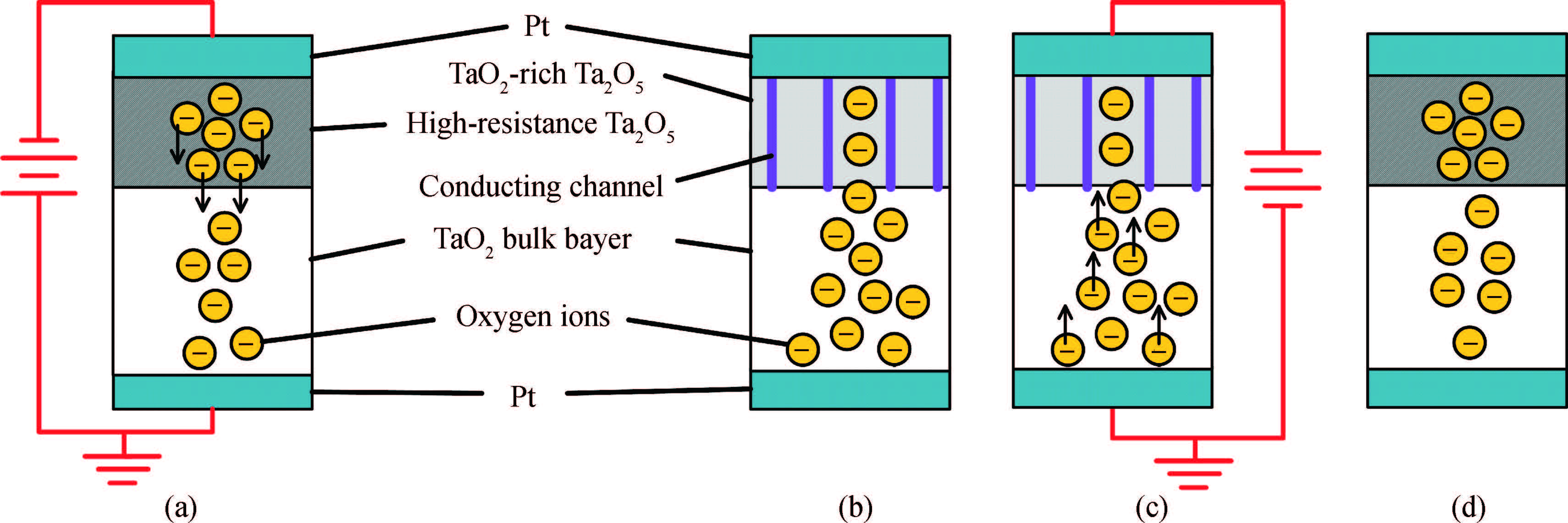
(a) A negative bias is applied on the top electrode to switch the device ON, repelling negatively charged oxygen ions away from the Ta2O5 layer towards the TaO2 layer. (b) The Ta2O5 phase is reduced to TaO and Ta. After low-resistance TaO and Ta phases align, it forms conducting channels in the Ta2O5 layer. (c) Positive bias is applied on the top electrode to switch the device OFF, attracting oxygen ions towards the Ta2O5 layer. (d) The oxygen ions oxidize TaO and Ta phases to become Ta2O5 phases, and cause the collapse of conducting channels.
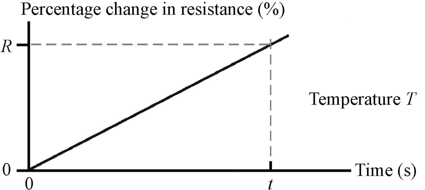
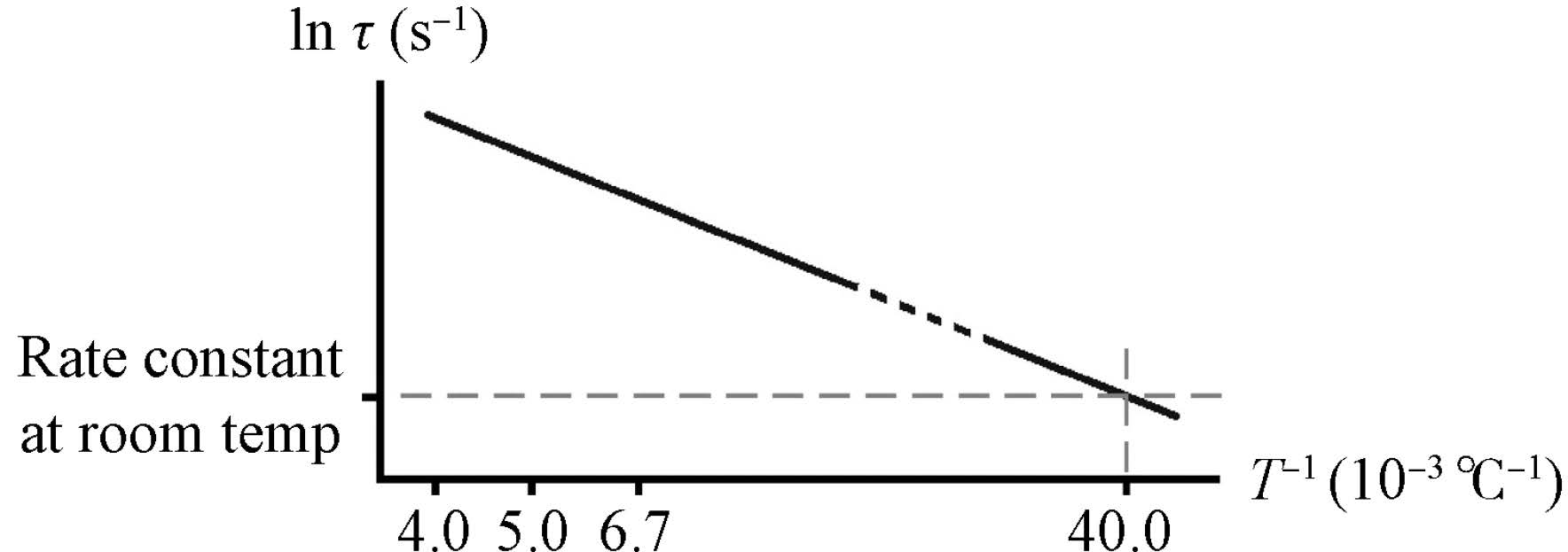
$40.0 \times10^{-3}$ ℃-1 corresponds to a room temperature of 25 °C,while 4.0,5.0 and 6.7 (×10-3) °C-1 corresponds to the temperature-accelerated degradation performed at 250,200,and 150 °C respectively.
Table 1. Gibbs free energy of the formation of metal oxides used in MIM resistive switching devices.
| Metal oxide | Gibbs free energy of formation,Δf G° (kJ/mol) |
| Hafnium oxide (HfO2) | 1088:2 |
| Zirconium oxide (ZrO2) | 1042:8 |
| Titanium oxide (TiO2) | 888:8 |
| Silicon oxide (SiO2) | 856:4 |
| Vanadium oxide (VO2) | 446:4 |
| Nickel oxide (NiO) | 211:7 |
| Tantalum oxide (TaO2) | 209:0 |
| Copper oxide (Cu2O) | 149:0 |
 DownLoad: CSV
Table 2. Window functions proposed for the behavior of charge carriers approaching electrode boundaries.
| Author(s) | Window function,f(x) |
| Strukov et al.[3] | f(x)=x(L-w)/L2 |
| Joglekar et al.[71] | f(x)=1-(2x-1)2p |
| Biolek et al.[73] | f(x)=1-(x-stp(-i))2p |
| Prodromakis et al.[74] | f(x)=1-[(x-0.5)2+0.75]p |
| Kvatinsky et al.[76] | $f_{\rm on} (x)=\exp\left[-\exp(-\frac{x-a_{\rm on}}{p})\right]$ |
| $f_{\rm off} (x)=\exp\left[-\exp(\frac{x-a_{\rm off}}{p})\right]$ |
DownLoad: CSV
| [1] |
Chua L. Memristor-the missing circuit element. IEEE Trans Circuit Theory, 1971, 18(5):507
|
| [2] |
Schroeder H, Jeong D S. Resistive switching in a Pt/TiO2/Pt thin film stack-a candidate for a non-volatile ReRAM. Microelectron Eng, 2007, 84(9-10):1982
|
| [3] |
Strukov D B, Snider G S, Stewart D R, et al. The missing memristor found. Nature, 2008, 453(1):80
|
| [4] |
Yang J J, Strukov D B, Stewart D R. Memristive devices for computing. Nat Nanotechnol, 2013, 8:13
|
| [5] |
Bez R, Pirovano A. Non-volatile memory technologies:emerging concepts and new materials. Mater Sci Semicond Process, 2004, 7(4-6):349
|
| [6] |
Duan S, Hu X, Wang L, et al. Memristor-based RRAM with applications. Sci China Inf Sci, 2012, 55(6):1446
|
| [7] |
Batas D, Fiedler H. A memristor SPICE implementation and a new approach for magnetic flux-controlled memristor modeling. IEEE Trans Nanotechnol, 2011, 10(2):250
|
| [8] |
Jo S H, Chang T, Ebong I, et al. Nanoscale memristor device as synapse in neuromorphic systems. Nano Lett, 2010, 10(4):1297
|
| [9] |
Vontobel P O, Robinett W, Kuekes P J, et al. Writing to and reading from a nano-scale crossbar memory based on memristors. Nanotechnology, 2009, 20(42):1
|
| [10] |
Eshraghian K, Cho K, Kavehei O, et al. Memristor MOS content addressable memory (MCAM):hybrid architecture for future high performance search engines. IEEE Trans VLSI, 2011, 19(8):1407
|
| [11] |
Yoshida C, Tsunoda K, Noshiro H, et al. High speed resistive switching in Pt/TiO2/TiN film for nonvolatile memory application. Appl Phys Lett, 2007, 91(22):223510
|
| [12] |
Yang J J, Miao F, Pickett M D, et al. The mechanism of electroforming of metal oxide memristive switches. Nanotechnology, 2009, 20(21):215201
|
| [13] |
Boboila S, Desnoyers P. Write endurance in flash drives:measurements and analysis. USENIX Conference on File and Storage Technologies, 2010:115
|
| [14] |
Rajachidambaram J S, Murali S, Conley J F, et al. Bipolar resistive switching in an amorphous zinc tin oxide memristive device. J Vac Sci Technol B, 2013, 31(1):01A104
|
| [15] |
Driscoll T, Kim H T, Chae B G, et al. Phase-transition driven memristive system. Appl Phys Lett, 2009, 95(4):043503
|
| [16] |
Yao J, Sun Z, Zhong L, et al. Resistive switches and memories from silicon oxide. Nano Lett, 2010, 10(10):4105
|
| [17] |
Chen A, Haddad S, Wu Y J, et al. Non-volatile resistive switching for advanced memory applications. IEEE International Electron Devices Meeting, 2005:746
|
| [18] |
Zhang X. Resistive switching characteristics of Ni/HfO2/Pt ReRAM. J Semicond, 2012, 33(5):054011
|
| [19] |
Sakamoto T, Banno N, Iguchi N, et al. A Ta2O5 solid-electrolyte switch with improved reliability. IEEE Symposium on VLSI Technology, 2007:38
|
| [20] |
Prakash A, Jana D, Maikap S. TaO_x-based resistive switching memories:prospective and challenges. Nanoscale Res Lett, 2013, 8(1):418
|
| [21] |
Yang J J, Zhang M X, Strachan J P, et al. High switching endurance in TaOX memristive devices. Appl Phys Lett, 2010, 97(23):232102
|
| [22] |
Akinaga H, Shima H. Resistive random access memory (ReRAM):a metal oxide memory cell. Proc IEEE, 2010:98(12):2237
|
| [23] |
Fujisaki Y. Overview of emerging semiconductor non-volatile memories. IEICE Electron Express, 2012, 9(10):908
|
| [24] |
Mazumder P, Kang S M, Waser R. Memristors:devices, models, and applications. Proc IEEE, 2012, 100(6):1911
|
| [25] |
Ho P W C, Hatem F O, Almurib H A F, et al. Comparison on TiO2 and TaO2 based bipolar resistive switching devices. IEEE International Conference on Electronic Design (ICED), 2014:249
|
| [26] |
Lee M J, Lee C B, Lee D, et al. A fast, high-endurance and scalable non-volatile memory device made from asymmetric Ta2O5-x/TaO2-x bilayer structures. Nat Mater, 2011, 10(8):625
|
| [27] |
Yoo H K, Kang B S, Lee S B. Forming time of conducting channels in double-layer Pt/Ta2O5/TaOx/Pt and single-layer Pt/TaOx/Pt resistance memories. Thin Solid Films, 2013, 540:190
|
| [28] |
Yoo H K, Lee S B, Lee J S, et al. Conversion from unipolar to bipolar resistance switching by inserting Ta2O5 layer in Pt/TaOX/Pt cells. Appl Phys Lett, 2011, 98(18):183507
|
| [29] |
Lee S B, Yoo H K, Kim K, et al. Forming mechanism of the bipolar resistance switching in double-layer memristive nanodevices. Nanotechnology, 2012, 23(31):315202
|
| [30] |
Wei Z, Kanzawa Y, Arita K, et al. Highly reliable TaOx ReRAM and direct evidence of redox reaction mechanism. IEEE International Electron Devices Meeting, 2008:1
|
| [31] |
Fukuda N, Fukuju K, Yogosawa I, et al. Forming-free resistance random access memory using Ta2O5/TaOx bi-layer prepared by magnetron sputtering method. MRS Proc, 2012, 1430
|
| [32] |
Pagnia H, Sotnik N. Bistable switching in electroformed metal-insulator-metal devices. Phys Status Solidi, 1988, 108(1):11
|
| [33] |
Collins R A, Bowman G, Sutherland R R. Electroforming of MIM thin-film devices in air at atmospheric pressure. J Phys D Appl Phys, 1971, 4(11):49
|
| [34] |
Dearnaley G, Stoneham A M, Morgan D V. Electrical phenomena in amorphous oxide films. Reports Prog Phys, 1970, 33(3):1129
|
| [35] |
Thurstans R E, Oxley D P. The electroformed metal-insulator-metal structure:a comprehensive model. J Phys D Appl Phys, 2002, 35(8):802
|
| [36] |
Strachan J P, Strukov D B, Borghetti J, et al. The switching location of a bipolar memristor:chemical, thermal and structural mapping. Nanotechnology, 2011, 22(25):254015
|
| [37] |
Münstermann R, Yang J J, Strachan J P, et al. Morphological and electrical changes in TiO2 memristive devices induced by electroforming and switching. Phys Status Solidi-Rapid Res Lett, 2010, 4(1/2):16
|
| [38] |
Dean J A. Lange's handbook of chemistry. 15th ed. New York, USA:McGraw-Hill, Inc, 1999
|
| [39] |
Lv H, Wang M, Wan H, et al. Endurance enhancement of Cu-oxide based resistive switching memory with Al top electrode. Appl Phys Lett, 2009, 94(21):213502
|
| [40] |
Nauenheim C, Kuegeler C, Ruediger A, et al. Investigation of the electroforming process in resistively switching TiO2 nanocrosspoint junctions. Appl Phys Lett, 2010, 96(12):122902
|
| [41] |
Kwon D H, Kim K M, Jang J H, et al. Atomic structure of conducting nanofilaments in TiO2 resistive switching memory. Nat Nanotechnol, 2010, 5:148
|
| [42] |
Miao F, Strachan J P, Yang J J, et al. Anatomy of a nanoscale conduction channel reveals the mechanism of a high-performance memristor. Adv Mater, 2011, 23(47):5633
|
| [43] |
Hosotani K, Park S G, Nishi Y. Electric field dependent switching and degradation of resistance random access memory. IEEE International Integrated Reliability Workshop Final Report, 2009:11
|
| [44] |
Dearnaley G, Morgan D V, Stoneham A M. A model for filament growth and switching in amorphous oxide films. J Non Cryst Solids, 1970, 4:593
|
| [45] |
Kim K M, Choi B J, Hwang C S. Localized switching mechanism in resistive switching of atomic-layer-deposited TiO2 thin films. Appl Phys Lett, 2007, 90(24):242906
|
| [46] |
Sire C, Blonkowski S, Gordon M J, et al. Statistics of electrical breakdown field in HfO2 and SiO2 films from millimeter to nanometer length scales. Appl Phys Lett, 2007, 91(24):242905
|
| [47] |
Murali S, Rajachidambaram J S, Han S Y, et al. Resistive switching in zinc-tin-oxide. Solid State Electron, 2013, 79:248
|
| [48] |
Yang M K, Park J W, Ko T K, et al. Resistive switching characteristics of TiN/MnO2/Pt memory devices. Phys Status Solidi-Rapid Res Lett, 2010, 4(8/9):233
|
| [49] |
Lu Y M, Noman M, Chen W, et al. Elimination of high transient currents and electrode damage during electroformation of TiO2-based resistive switching devices. J Phys D Appl Phys, 2012, 45(39):395101
|
| [50] |
Salaoru I, Prodromakis T, Khiat A, et al. Resistive switching of oxygen enhanced TiO2 thin-film devices. Appl Phys Lett, 2013, 102(1):013506
|
| [51] |
Huang J J, Kuo C W, Chang W C, et al. Transition of stable rectification to resistive-switching in Ti/TiO2/Pt oxide diode. Appl Phys Lett, 2010, 96(26):262901
|
| [52] |
Hudec B, Hranai M, Hušeková K, et al. Resistive switching in RuO2/TiO2/RuO2 MIM structures for non-volatile memory application. International Conference on Advanced Semiconductor Devices & Microsystems, 2010:255
|
| [53] |
Choi B J, Jeong D S, Kim S K, et al. Resistive switching mechanism of TiO2 thin films grown by atomic-layer deposition. J Appl Phys, 2005, 98(3):033715
|
| [54] |
Do Y H, Kwak J S, Hong J P, et al. Al electrode dependent transition to bipolar resistive switching characteristics in pure TiO2 films. J Appl Phys, 2008, 104(11):114512
|
| [55] |
Strachan J P, Pickett M D, Yang J J, et al. Direct identification of the conducting channels in a functioning memristive device. Adv Mater, 2010, 22(32):3573
|
| [56] |
Yang J J, Pickett M D, Li X, et al. Memristive switching mechanism for metal/oxide/metal nanodevices. Nat Nanotechnol, 2008, 3(7):429
|
| [57] |
Sawa A. Resistive switching in transition metal oxides. Mater today, 2008, 11(6):28
|
| [58] |
Yasuhara R, Fujiwara K, Horiba K, et al. Inhomogeneous chemical states in resistance-switching devices with a planar-type Pt/CuO/Pt structure. Appl Phys Lett, 2009, 95(1):012110
|
| [59] |
Sun P, Su L, Ling L, et al. Simulation study of conductive filament growth dynamics in oxide-electrolyte-based ReRAM. J Semicond, 2014, 35(10):104007
|
| [60] |
Park G S, Kim Y B, Park S Y, et al. In situ observation of filamentary conducting channels in an asymmetric Ta2O5-x/TaO2-x bilayer structure. Nat Commun, 2013, 4:2382
|
| [61] |
Strachan J P, Medeiros-Ribeiro G, Yang J J, et al. Spectromicroscopy of tantalum oxide memristors. Appl Phys Lett, 2011, 98(24):242114
|
| [62] |
Bi J, Han Z. Characteristics of HfO2/Hf-based bipolar resistive memories. J Semicond, 2015, 36(6):064010
|
| [63] |
Kim K M, Choi B J, Shin Y C, et al. Anode-interface localized filamentary mechanism in resistive switching of TiO2 thin films. Appl Phys Lett, 2007, 91(1):012907
|
| [64] |
Lin C Y, Wu C Y, Wu C Y, et al. Modified resistive switching behavior of ZrO2 memory films based on the interface layer formed by using Ti top electrode. J Appl Phys, 2007, 102(9):094101
|
| [65] |
Prakash A, Maikap S, Chiu H C, et al. Enhanced resistive switching memory characteristics and mechanism using a Ti nanolayer at the W/TaOX interface. Nanoscale Res Lett, 2014, 9(1):125
|
| [66] |
Zhuo V Y, Jiang Y, Zhao R, et al. Improved switching uniformity and low-voltage operation in TaO-based RRAM using Ge reactive layer. IEEE Electron Device Lett, 2013,34(9):1130
|
| [67] |
Seong D, Jo M, Lee D, et al. HPHA effect on reversible resistive switching of Pt/Nb-doped SrTiO3 Schottky junction for nonvolatile memory application. Electrochem Solid-State Lett, 2007, 10(6):168
|
| [68] |
Hatem F O, Ho P W C, Kumar T N, et al. Modeling of bipolar resistive switching of a nonlinear MISM memristor. Semicond Sci Technol, 2015, 30(11):115009
|
| [69] |
Kim S, Choi S, Lu W. Comprehensive physical model of dynamic resistive switching in an oxide memristor. ACS Nano, 2014
|
| [70] |
Mattsson M S, Niklasson G A, Forsgren K, et al. A frequency response and transient current study of ��-Ta2O5:methods of estimating the dielectric constant, direct current conductivity, and ion mobility. J Appl Phys, 1999, 85(4):2185
|
| [71] |
Joglekar Y N, Wolf S J. The elusive memristor:properties of basic electrical circuits. Eur J Phys, 2009, 30(4):661
|
| [72] |
Strukov D B, Williams R S. Exponential ionic drift:fast switching and low volatility of thin-film memristors. Appl Phys A, 2009, 94(3):515
|
| [73] |
Biolek Z, Biolek D, Biolková V. SPICE model of memristor with nonlinear dopant drift. Radio Engineering, 2009, 18(2):210
|
| [74] |
Prodromakis T, Peh B P, Papavassiliou C, et al. A versatile memristor model with non-linear dopant kinetics. IEEE Trans Electron Devices, 2011, 58(9):3099
|
| [75] |
Rossel C, Meijer G I, Breìmaud D, et al. Electrical current distribution across a metal-insulator-metal structure during bistable switching. J Appl Phys, 2001, 90(6):2892
|
| [76] |
Kvatinsky S, Friedman E G, Kolodny A, et al. TEAM:threshold adaptive memristor model. IEEE Trans Circuits Syst I, 2013, 60(1):211
|
| [77] |
Zhang L, Chen Z, Yang J J, et al. A compact modeling of TiO2-TiO2-x memristor. Appl Phys Lett, 2013, 102(15):153503
|
| [78] |
Sze S M, Ng K K. Physics of semiconductor devices. 3rd ed. New Jersey, USA:John Wiley & Sons, 2007
|
| [79] |
Ji H H, Lee M J, Chang L B, et al. Modeling for bipolar resistive memory switching in transition-metal oxides. Phys Rev B, 2010, 82(15):155321
|
| [80] |
Pickett M D, Strukov D B, Borghetti J L, et al. Switching dynamics in titanium dioxide memristive devices. J Appl Phys, 2009, 106(7):074508
|
| [81] |
Zhang F, Gan X, Li X, et al. Realization of rectifying and resistive switching behaviors of TiO2 nanorod arrays for nonvolatile memory. Electrochem Solid-State Lett, 2011, 14(10):H422
|
| [82] |
Acharyya D, Hazra A, Bhattacharyya P. A journey towards reliability improvement of TiO2 based resistive random access memory:a review. Microelectron Reliab, 2014, 54(3):541
|
| [83] |
Franke E, Trimble C L, DeVries M J, et al. Dielectric function of amorphous tantalum oxide from the far infrared to the deep ultraviolet spectral region measured by spectroscopic ellipsometry. J Appl Phys, 2000, 88(9):5166
|
| [84] |
Kukli K, Aarik J, Aidla A, et al. Properties of tantalum oxide thin films grown by atomic layer deposition. Thin Solid Films, 1995, 260(2):135
|
| [85] |
Fleming R M, Lang D V, Jones C D W, et al. Defect dominated charge transport in amorphous Ta2O5 thin films. J Appl Phys, 2000, 88(2):850
|
| [86] |
Cao X, Li X, Yu W, et al. Bipolar resistive switching properties of microcrystalline TiO2 thin films deposited by pulsed laser deposition. Mater Sci Eng B, 2009, 157(1-3):36
|
| [87] |
Blaschke D, Zahn P, Skorupa I, et al. Resistive switching in thermally oxidized titanium films. International Semiconductor Conference Dresden-Grenoble (ISCDG), 2013:1
|
| [88] |
Lee S R, Kim Y, Chang M, et al. Multi-level switching of triple-layered TaO_x RRAM with excellent reliability for storage class memory. Symposium on VLSI Technology, 2012:71
|
| [89] |
Hsiung C P, Gan J Y, Tseng S H, et al. Resistance switching characteristics of TiO2 thin films prepared with reactive sputtering. Electrochem. Solid-State Lett, 2009, 12(7):G31
|
| [90] |
Niset M, Kuhn P. Typical data retention for nonvolatile memory. Freescale Semiconductor Engineering Bulletin, 2005:EB618/D
|
| [91] |
Jo S H, Kim K H, Lu W. Programmable resistance switching in nanoscale two-terminal devices. nano Lett, 2009, 9:496
|
| [92] |
Chen A, Haddad S, Wu Y C. A temperature-accelerated method to evaluate data retention of resistive switching nonvolatile memory. IEEE Electron Device Lett, 2008, 29(1):38
|
| [93] |
Young H Do, June S K, Yoon C B, et al. Hysteretic bipolar resistive switching characteristics in TiO2-TiO2-x multilayer homojunctions. Appl Phys Lett, 2009, 95(9):093507
|
| [94] |
Jung S, Kong J, Song S, et al. Resistive switching characteristics of solution-processed transparent TiO_x for nonvolatile memory application. J Electrochem Soc, 2010, 157(11):1042
|
| [95] |
Chang W Y, Cheng K J, Tsai J M, et al. Improvement of resistive switching characteristics in TiO2 thin films with embedded Pt nanocrystals. Appl Phys Lett, 2009, 95(4):042104
|
| [96] |
Xia Q, Pickett M D, Yang J J, et al. Impact of geometry on the performance of memristive nanodevices. Nanotechnology, 2011, 22(25):254026
|
| [97] |
Okamoto H. O-Ti (oxygen-titanium). J Phase Equilibria Diffus, 2011, 32(5):473
|
| [98] |
Garg S P, Krishnamurthy N, Awasthi A, et al. The O-Ta (oxygen-Tantalum) system. J Phase Equilibria, 1996, 17(1):63
|
| [99] |
Kihlborg L, Olovsson I. Arne Magnéli, 1914-1996. Acta Cryst A, 1997, 53(2):103
|
| [100] |
Yang J J, Strachan J P, Xia Q, et al. Diffusion of adhesion layer metals controls nanoscale memristive switching. Adv Mater, 2010, 22(36):4034
|
| [101] |
Park J, Jung S, Lee J, et al. Resistive switching characteristics of ultra-thin TiO_x. Microelectron Eng, 2011, 88(7):1136
|
| [102] |
Lee T W, Nickel J H. Memristor resistance modulation for analog applications. IEEE Electron Device Lett, 2012, 33(10):1456
|
| [103] |
Tedesco J L, Stephey L, Hernández-Mora M, et al. Switching mechanisms in flexible solution-processed TiO2 memristors. Nanotechnology, 2012, 23(30):305206
|
| [104] |
Lv H B, Yin M, Fu X F, et al. Resistive memory switching of CuXO films for a nonvolatile memory application. IEEE Electron Device Lett, 2008, 29(4):309
|
| [105] |
Gu T. Role of oxygen vacancies in TiO2-based resistive switches. J Appl Phys, 2013, 113(3):033707
|
| [106] |
Ko D S, Kim S I, Ahn T Y, et al. Effect of the electrode materials on the resistive switching of Ti4O7. Appl Phys Lett, 2012, 101(5):053502
|
| [107] |
Lin K L, Hou T H, Shieh J, et al. Electrode dependence of filament formation in HfO2 resistive-switching memory. J Appl Phys, 2011, 109(8):084104
|
| [108] |
Jeong H Y, Kim Y I, Lee J Y, et al. Choi, A low-temperature-grown TiO2-based device for the flexible stacked RRAM application. Nanotechnology, 2010, 21(11):115203
|
| [109] |
Biju K P, Liu X, Bourim E M, et al. Asymmetric bipolar resistive switching in solution-processed Pt/TiO2/W devices. J Phys D Appl Phys, 2010, 43(49):495104
|
| [110] |
Chen C, Gao S, Zeng F, et al. Migration of interfacial oxygen ions modulated resistive switching in oxide-based memory devices. J Appl Phys, 2013, 114(1):014502
|
| [111] |
Yoon M J, Lee S B, Yoo H K, et al. Dielectric-breakdown-like forming process in the unipolar resistance switching of Ta2O5-X thin films. Curr Appl Phys, 2012, 1293:846
|
| [112] |
Prakash A, Maikap S, Chen G, et al. Improvement of high-�� Ta2O5-based resistive switching memory using Ti interfacial layer. International Symposium on VLSI Technology, Systems and Applications (VLSI-TSA), 2011:1
|
| [113] |
Hernández-Rodríguez E, Márquez-Herrera A, Zaleta-Alejandre E, et al. Effect of electrode type in the resistive switching behaviour of TiO2 thin films. J Phys D Appl Phys, 2013, 46(4):045103
|
| [114] |
Schindler C, Thermadam S C P, Waser R, et al. Bipolar and unipolar resistive switching in Cu-doped SiO2. IEEE Trans Electron Devices, 2007, 54(10):2762
|
| [115] |
Saura X, Lian X, Jiménez D, et al. Field-effect control of breakdown paths in HfO2 based MIM structures. Microelectron Reliab, 2013, 53(9-11):1346
|


Article views: 6293 Times PDF downloads: 83 Times Cited by: 0 Times
Received: 15 September 2015 Revised: 06 December 2015 Online: Published: 01 June 2016
| Citation: |
Patrick W. C. Ho, Firas Odai Hatem, Haider Abbas F. Almurib, T. Nandha Kumar. Comparison between Pt/TiO2/Pt and Pt/TaOX/TaOY/Pt based bipolar resistive switching devices[J]. Journal of Semiconductors, 2016, 37(6): 064001. doi: 10.1088/1674-4926/37/6/064001
****
P. W. C. Ho, F O Hatem, H. A. F. Almurib, T. N. Kumar. Comparison between Pt/TiO2/Pt and Pt/TaOX/TaOY/Pt based bipolar resistive switching devices[J]. J. Semicond., 2016, 37(6): 064001. doi: 10.1088/1674-4926/37/6/064001.

|
| [1] |
Chua L. Memristor-the missing circuit element. IEEE Trans Circuit Theory, 1971, 18(5):507
|
| [2] |
Schroeder H, Jeong D S. Resistive switching in a Pt/TiO2/Pt thin film stack-a candidate for a non-volatile ReRAM. Microelectron Eng, 2007, 84(9-10):1982
|
| [3] |
Strukov D B, Snider G S, Stewart D R, et al. The missing memristor found. Nature, 2008, 453(1):80
|
| [4] |
Yang J J, Strukov D B, Stewart D R. Memristive devices for computing. Nat Nanotechnol, 2013, 8:13
|
| [5] |
Bez R, Pirovano A. Non-volatile memory technologies:emerging concepts and new materials. Mater Sci Semicond Process, 2004, 7(4-6):349
|
| [6] |
Duan S, Hu X, Wang L, et al. Memristor-based RRAM with applications. Sci China Inf Sci, 2012, 55(6):1446
|
| [7] |
Batas D, Fiedler H. A memristor SPICE implementation and a new approach for magnetic flux-controlled memristor modeling. IEEE Trans Nanotechnol, 2011, 10(2):250
|
| [8] |
Jo S H, Chang T, Ebong I, et al. Nanoscale memristor device as synapse in neuromorphic systems. Nano Lett, 2010, 10(4):1297
|
| [9] |
Vontobel P O, Robinett W, Kuekes P J, et al. Writing to and reading from a nano-scale crossbar memory based on memristors. Nanotechnology, 2009, 20(42):1
|
| [10] |
Eshraghian K, Cho K, Kavehei O, et al. Memristor MOS content addressable memory (MCAM):hybrid architecture for future high performance search engines. IEEE Trans VLSI, 2011, 19(8):1407
|
| [11] |
Yoshida C, Tsunoda K, Noshiro H, et al. High speed resistive switching in Pt/TiO2/TiN film for nonvolatile memory application. Appl Phys Lett, 2007, 91(22):223510
|
| [12] |
Yang J J, Miao F, Pickett M D, et al. The mechanism of electroforming of metal oxide memristive switches. Nanotechnology, 2009, 20(21):215201
|
| [13] |
Boboila S, Desnoyers P. Write endurance in flash drives:measurements and analysis. USENIX Conference on File and Storage Technologies, 2010:115
|
| [14] |
Rajachidambaram J S, Murali S, Conley J F, et al. Bipolar resistive switching in an amorphous zinc tin oxide memristive device. J Vac Sci Technol B, 2013, 31(1):01A104
|
| [15] |
Driscoll T, Kim H T, Chae B G, et al. Phase-transition driven memristive system. Appl Phys Lett, 2009, 95(4):043503
|
| [16] |
Yao J, Sun Z, Zhong L, et al. Resistive switches and memories from silicon oxide. Nano Lett, 2010, 10(10):4105
|
| [17] |
Chen A, Haddad S, Wu Y J, et al. Non-volatile resistive switching for advanced memory applications. IEEE International Electron Devices Meeting, 2005:746
|
| [18] |
Zhang X. Resistive switching characteristics of Ni/HfO2/Pt ReRAM. J Semicond, 2012, 33(5):054011
|
| [19] |
Sakamoto T, Banno N, Iguchi N, et al. A Ta2O5 solid-electrolyte switch with improved reliability. IEEE Symposium on VLSI Technology, 2007:38
|
| [20] |
Prakash A, Jana D, Maikap S. TaO_x-based resistive switching memories:prospective and challenges. Nanoscale Res Lett, 2013, 8(1):418
|
| [21] |
Yang J J, Zhang M X, Strachan J P, et al. High switching endurance in TaOX memristive devices. Appl Phys Lett, 2010, 97(23):232102
|
| [22] |
Akinaga H, Shima H. Resistive random access memory (ReRAM):a metal oxide memory cell. Proc IEEE, 2010:98(12):2237
|
| [23] |
Fujisaki Y. Overview of emerging semiconductor non-volatile memories. IEICE Electron Express, 2012, 9(10):908
|
| [24] |
Mazumder P, Kang S M, Waser R. Memristors:devices, models, and applications. Proc IEEE, 2012, 100(6):1911
|
| [25] |
Ho P W C, Hatem F O, Almurib H A F, et al. Comparison on TiO2 and TaO2 based bipolar resistive switching devices. IEEE International Conference on Electronic Design (ICED), 2014:249
|
| [26] |
Lee M J, Lee C B, Lee D, et al. A fast, high-endurance and scalable non-volatile memory device made from asymmetric Ta2O5-x/TaO2-x bilayer structures. Nat Mater, 2011, 10(8):625
|
| [27] |
Yoo H K, Kang B S, Lee S B. Forming time of conducting channels in double-layer Pt/Ta2O5/TaOx/Pt and single-layer Pt/TaOx/Pt resistance memories. Thin Solid Films, 2013, 540:190
|
| [28] |
Yoo H K, Lee S B, Lee J S, et al. Conversion from unipolar to bipolar resistance switching by inserting Ta2O5 layer in Pt/TaOX/Pt cells. Appl Phys Lett, 2011, 98(18):183507
|
| [29] |
Lee S B, Yoo H K, Kim K, et al. Forming mechanism of the bipolar resistance switching in double-layer memristive nanodevices. Nanotechnology, 2012, 23(31):315202
|
| [30] |
Wei Z, Kanzawa Y, Arita K, et al. Highly reliable TaOx ReRAM and direct evidence of redox reaction mechanism. IEEE International Electron Devices Meeting, 2008:1
|
| [31] |
Fukuda N, Fukuju K, Yogosawa I, et al. Forming-free resistance random access memory using Ta2O5/TaOx bi-layer prepared by magnetron sputtering method. MRS Proc, 2012, 1430
|
| [32] |
Pagnia H, Sotnik N. Bistable switching in electroformed metal-insulator-metal devices. Phys Status Solidi, 1988, 108(1):11
|
| [33] |
Collins R A, Bowman G, Sutherland R R. Electroforming of MIM thin-film devices in air at atmospheric pressure. J Phys D Appl Phys, 1971, 4(11):49
|
| [34] |
Dearnaley G, Stoneham A M, Morgan D V. Electrical phenomena in amorphous oxide films. Reports Prog Phys, 1970, 33(3):1129
|
| [35] |
Thurstans R E, Oxley D P. The electroformed metal-insulator-metal structure:a comprehensive model. J Phys D Appl Phys, 2002, 35(8):802
|
| [36] |
Strachan J P, Strukov D B, Borghetti J, et al. The switching location of a bipolar memristor:chemical, thermal and structural mapping. Nanotechnology, 2011, 22(25):254015
|
| [37] |
Münstermann R, Yang J J, Strachan J P, et al. Morphological and electrical changes in TiO2 memristive devices induced by electroforming and switching. Phys Status Solidi-Rapid Res Lett, 2010, 4(1/2):16
|
| [38] |
Dean J A. Lange's handbook of chemistry. 15th ed. New York, USA:McGraw-Hill, Inc, 1999
|
| [39] |
Lv H, Wang M, Wan H, et al. Endurance enhancement of Cu-oxide based resistive switching memory with Al top electrode. Appl Phys Lett, 2009, 94(21):213502
|
| [40] |
Nauenheim C, Kuegeler C, Ruediger A, et al. Investigation of the electroforming process in resistively switching TiO2 nanocrosspoint junctions. Appl Phys Lett, 2010, 96(12):122902
|
| [41] |
Kwon D H, Kim K M, Jang J H, et al. Atomic structure of conducting nanofilaments in TiO2 resistive switching memory. Nat Nanotechnol, 2010, 5:148
|
| [42] |
Miao F, Strachan J P, Yang J J, et al. Anatomy of a nanoscale conduction channel reveals the mechanism of a high-performance memristor. Adv Mater, 2011, 23(47):5633
|
| [43] |
Hosotani K, Park S G, Nishi Y. Electric field dependent switching and degradation of resistance random access memory. IEEE International Integrated Reliability Workshop Final Report, 2009:11
|
| [44] |
Dearnaley G, Morgan D V, Stoneham A M. A model for filament growth and switching in amorphous oxide films. J Non Cryst Solids, 1970, 4:593
|
| [45] |
Kim K M, Choi B J, Hwang C S. Localized switching mechanism in resistive switching of atomic-layer-deposited TiO2 thin films. Appl Phys Lett, 2007, 90(24):242906
|
| [46] |
Sire C, Blonkowski S, Gordon M J, et al. Statistics of electrical breakdown field in HfO2 and SiO2 films from millimeter to nanometer length scales. Appl Phys Lett, 2007, 91(24):242905
|
| [47] |
Murali S, Rajachidambaram J S, Han S Y, et al. Resistive switching in zinc-tin-oxide. Solid State Electron, 2013, 79:248
|
| [48] |
Yang M K, Park J W, Ko T K, et al. Resistive switching characteristics of TiN/MnO2/Pt memory devices. Phys Status Solidi-Rapid Res Lett, 2010, 4(8/9):233
|
| [49] |
Lu Y M, Noman M, Chen W, et al. Elimination of high transient currents and electrode damage during electroformation of TiO2-based resistive switching devices. J Phys D Appl Phys, 2012, 45(39):395101
|
| [50] |
Salaoru I, Prodromakis T, Khiat A, et al. Resistive switching of oxygen enhanced TiO2 thin-film devices. Appl Phys Lett, 2013, 102(1):013506
|
| [51] |
Huang J J, Kuo C W, Chang W C, et al. Transition of stable rectification to resistive-switching in Ti/TiO2/Pt oxide diode. Appl Phys Lett, 2010, 96(26):262901
|
| [52] |
Hudec B, Hranai M, Hušeková K, et al. Resistive switching in RuO2/TiO2/RuO2 MIM structures for non-volatile memory application. International Conference on Advanced Semiconductor Devices & Microsystems, 2010:255
|
| [53] |
Choi B J, Jeong D S, Kim S K, et al. Resistive switching mechanism of TiO2 thin films grown by atomic-layer deposition. J Appl Phys, 2005, 98(3):033715
|
| [54] |
Do Y H, Kwak J S, Hong J P, et al. Al electrode dependent transition to bipolar resistive switching characteristics in pure TiO2 films. J Appl Phys, 2008, 104(11):114512
|
| [55] |
Strachan J P, Pickett M D, Yang J J, et al. Direct identification of the conducting channels in a functioning memristive device. Adv Mater, 2010, 22(32):3573
|
| [56] |
Yang J J, Pickett M D, Li X, et al. Memristive switching mechanism for metal/oxide/metal nanodevices. Nat Nanotechnol, 2008, 3(7):429
|
| [57] |
Sawa A. Resistive switching in transition metal oxides. Mater today, 2008, 11(6):28
|
| [58] |
Yasuhara R, Fujiwara K, Horiba K, et al. Inhomogeneous chemical states in resistance-switching devices with a planar-type Pt/CuO/Pt structure. Appl Phys Lett, 2009, 95(1):012110
|
| [59] |
Sun P, Su L, Ling L, et al. Simulation study of conductive filament growth dynamics in oxide-electrolyte-based ReRAM. J Semicond, 2014, 35(10):104007
|
| [60] |
Park G S, Kim Y B, Park S Y, et al. In situ observation of filamentary conducting channels in an asymmetric Ta2O5-x/TaO2-x bilayer structure. Nat Commun, 2013, 4:2382
|
| [61] |
Strachan J P, Medeiros-Ribeiro G, Yang J J, et al. Spectromicroscopy of tantalum oxide memristors. Appl Phys Lett, 2011, 98(24):242114
|
| [62] |
Bi J, Han Z. Characteristics of HfO2/Hf-based bipolar resistive memories. J Semicond, 2015, 36(6):064010
|
| [63] |
Kim K M, Choi B J, Shin Y C, et al. Anode-interface localized filamentary mechanism in resistive switching of TiO2 thin films. Appl Phys Lett, 2007, 91(1):012907
|
| [64] |
Lin C Y, Wu C Y, Wu C Y, et al. Modified resistive switching behavior of ZrO2 memory films based on the interface layer formed by using Ti top electrode. J Appl Phys, 2007, 102(9):094101
|
| [65] |
Prakash A, Maikap S, Chiu H C, et al. Enhanced resistive switching memory characteristics and mechanism using a Ti nanolayer at the W/TaOX interface. Nanoscale Res Lett, 2014, 9(1):125
|
| [66] |
Zhuo V Y, Jiang Y, Zhao R, et al. Improved switching uniformity and low-voltage operation in TaO-based RRAM using Ge reactive layer. IEEE Electron Device Lett, 2013,34(9):1130
|
| [67] |
Seong D, Jo M, Lee D, et al. HPHA effect on reversible resistive switching of Pt/Nb-doped SrTiO3 Schottky junction for nonvolatile memory application. Electrochem Solid-State Lett, 2007, 10(6):168
|
| [68] |
Hatem F O, Ho P W C, Kumar T N, et al. Modeling of bipolar resistive switching of a nonlinear MISM memristor. Semicond Sci Technol, 2015, 30(11):115009
|
| [69] |
Kim S, Choi S, Lu W. Comprehensive physical model of dynamic resistive switching in an oxide memristor. ACS Nano, 2014
|
| [70] |
Mattsson M S, Niklasson G A, Forsgren K, et al. A frequency response and transient current study of ��-Ta2O5:methods of estimating the dielectric constant, direct current conductivity, and ion mobility. J Appl Phys, 1999, 85(4):2185
|
| [71] |
Joglekar Y N, Wolf S J. The elusive memristor:properties of basic electrical circuits. Eur J Phys, 2009, 30(4):661
|
| [72] |
Strukov D B, Williams R S. Exponential ionic drift:fast switching and low volatility of thin-film memristors. Appl Phys A, 2009, 94(3):515
|
| [73] |
Biolek Z, Biolek D, Biolková V. SPICE model of memristor with nonlinear dopant drift. Radio Engineering, 2009, 18(2):210
|
| [74] |
Prodromakis T, Peh B P, Papavassiliou C, et al. A versatile memristor model with non-linear dopant kinetics. IEEE Trans Electron Devices, 2011, 58(9):3099
|
| [75] |
Rossel C, Meijer G I, Breìmaud D, et al. Electrical current distribution across a metal-insulator-metal structure during bistable switching. J Appl Phys, 2001, 90(6):2892
|
| [76] |
Kvatinsky S, Friedman E G, Kolodny A, et al. TEAM:threshold adaptive memristor model. IEEE Trans Circuits Syst I, 2013, 60(1):211
|
| [77] |
Zhang L, Chen Z, Yang J J, et al. A compact modeling of TiO2-TiO2-x memristor. Appl Phys Lett, 2013, 102(15):153503
|
| [78] |
Sze S M, Ng K K. Physics of semiconductor devices. 3rd ed. New Jersey, USA:John Wiley & Sons, 2007
|
| [79] |
Ji H H, Lee M J, Chang L B, et al. Modeling for bipolar resistive memory switching in transition-metal oxides. Phys Rev B, 2010, 82(15):155321
|
| [80] |
Pickett M D, Strukov D B, Borghetti J L, et al. Switching dynamics in titanium dioxide memristive devices. J Appl Phys, 2009, 106(7):074508
|
| [81] |
Zhang F, Gan X, Li X, et al. Realization of rectifying and resistive switching behaviors of TiO2 nanorod arrays for nonvolatile memory. Electrochem Solid-State Lett, 2011, 14(10):H422
|
| [82] |
Acharyya D, Hazra A, Bhattacharyya P. A journey towards reliability improvement of TiO2 based resistive random access memory:a review. Microelectron Reliab, 2014, 54(3):541
|
| [83] |
Franke E, Trimble C L, DeVries M J, et al. Dielectric function of amorphous tantalum oxide from the far infrared to the deep ultraviolet spectral region measured by spectroscopic ellipsometry. J Appl Phys, 2000, 88(9):5166
|
| [84] |
Kukli K, Aarik J, Aidla A, et al. Properties of tantalum oxide thin films grown by atomic layer deposition. Thin Solid Films, 1995, 260(2):135
|
| [85] |
Fleming R M, Lang D V, Jones C D W, et al. Defect dominated charge transport in amorphous Ta2O5 thin films. J Appl Phys, 2000, 88(2):850
|
| [86] |
Cao X, Li X, Yu W, et al. Bipolar resistive switching properties of microcrystalline TiO2 thin films deposited by pulsed laser deposition. Mater Sci Eng B, 2009, 157(1-3):36
|
| [87] |
Blaschke D, Zahn P, Skorupa I, et al. Resistive switching in thermally oxidized titanium films. International Semiconductor Conference Dresden-Grenoble (ISCDG), 2013:1
|
| [88] |
Lee S R, Kim Y, Chang M, et al. Multi-level switching of triple-layered TaO_x RRAM with excellent reliability for storage class memory. Symposium on VLSI Technology, 2012:71
|
| [89] |
Hsiung C P, Gan J Y, Tseng S H, et al. Resistance switching characteristics of TiO2 thin films prepared with reactive sputtering. Electrochem. Solid-State Lett, 2009, 12(7):G31
|
| [90] |
Niset M, Kuhn P. Typical data retention for nonvolatile memory. Freescale Semiconductor Engineering Bulletin, 2005:EB618/D
|
| [91] |
Jo S H, Kim K H, Lu W. Programmable resistance switching in nanoscale two-terminal devices. nano Lett, 2009, 9:496
|
| [92] |
Chen A, Haddad S, Wu Y C. A temperature-accelerated method to evaluate data retention of resistive switching nonvolatile memory. IEEE Electron Device Lett, 2008, 29(1):38
|
| [93] |
Young H Do, June S K, Yoon C B, et al. Hysteretic bipolar resistive switching characteristics in TiO2-TiO2-x multilayer homojunctions. Appl Phys Lett, 2009, 95(9):093507
|
| [94] |
Jung S, Kong J, Song S, et al. Resistive switching characteristics of solution-processed transparent TiO_x for nonvolatile memory application. J Electrochem Soc, 2010, 157(11):1042
|
| [95] |
Chang W Y, Cheng K J, Tsai J M, et al. Improvement of resistive switching characteristics in TiO2 thin films with embedded Pt nanocrystals. Appl Phys Lett, 2009, 95(4):042104
|
| [96] |
Xia Q, Pickett M D, Yang J J, et al. Impact of geometry on the performance of memristive nanodevices. Nanotechnology, 2011, 22(25):254026
|
| [97] |
Okamoto H. O-Ti (oxygen-titanium). J Phase Equilibria Diffus, 2011, 32(5):473
|
| [98] |
Garg S P, Krishnamurthy N, Awasthi A, et al. The O-Ta (oxygen-Tantalum) system. J Phase Equilibria, 1996, 17(1):63
|
| [99] |
Kihlborg L, Olovsson I. Arne Magnéli, 1914-1996. Acta Cryst A, 1997, 53(2):103
|
| [100] |
Yang J J, Strachan J P, Xia Q, et al. Diffusion of adhesion layer metals controls nanoscale memristive switching. Adv Mater, 2010, 22(36):4034
|
| [101] |
Park J, Jung S, Lee J, et al. Resistive switching characteristics of ultra-thin TiO_x. Microelectron Eng, 2011, 88(7):1136
|
| [102] |
Lee T W, Nickel J H. Memristor resistance modulation for analog applications. IEEE Electron Device Lett, 2012, 33(10):1456
|
| [103] |
Tedesco J L, Stephey L, Hernández-Mora M, et al. Switching mechanisms in flexible solution-processed TiO2 memristors. Nanotechnology, 2012, 23(30):305206
|
| [104] |
Lv H B, Yin M, Fu X F, et al. Resistive memory switching of CuXO films for a nonvolatile memory application. IEEE Electron Device Lett, 2008, 29(4):309
|
| [105] |
Gu T. Role of oxygen vacancies in TiO2-based resistive switches. J Appl Phys, 2013, 113(3):033707
|
| [106] |
Ko D S, Kim S I, Ahn T Y, et al. Effect of the electrode materials on the resistive switching of Ti4O7. Appl Phys Lett, 2012, 101(5):053502
|
| [107] |
Lin K L, Hou T H, Shieh J, et al. Electrode dependence of filament formation in HfO2 resistive-switching memory. J Appl Phys, 2011, 109(8):084104
|
| [108] |
Jeong H Y, Kim Y I, Lee J Y, et al. Choi, A low-temperature-grown TiO2-based device for the flexible stacked RRAM application. Nanotechnology, 2010, 21(11):115203
|
| [109] |
Biju K P, Liu X, Bourim E M, et al. Asymmetric bipolar resistive switching in solution-processed Pt/TiO2/W devices. J Phys D Appl Phys, 2010, 43(49):495104
|
| [110] |
Chen C, Gao S, Zeng F, et al. Migration of interfacial oxygen ions modulated resistive switching in oxide-based memory devices. J Appl Phys, 2013, 114(1):014502
|
| [111] |
Yoon M J, Lee S B, Yoo H K, et al. Dielectric-breakdown-like forming process in the unipolar resistance switching of Ta2O5-X thin films. Curr Appl Phys, 2012, 1293:846
|
| [112] |
Prakash A, Maikap S, Chen G, et al. Improvement of high-�� Ta2O5-based resistive switching memory using Ti interfacial layer. International Symposium on VLSI Technology, Systems and Applications (VLSI-TSA), 2011:1
|
| [113] |
Hernández-Rodríguez E, Márquez-Herrera A, Zaleta-Alejandre E, et al. Effect of electrode type in the resistive switching behaviour of TiO2 thin films. J Phys D Appl Phys, 2013, 46(4):045103
|
| [114] |
Schindler C, Thermadam S C P, Waser R, et al. Bipolar and unipolar resistive switching in Cu-doped SiO2. IEEE Trans Electron Devices, 2007, 54(10):2762
|
| [115] |
Saura X, Lian X, Jiménez D, et al. Field-effect control of breakdown paths in HfO2 based MIM structures. Microelectron Reliab, 2013, 53(9-11):1346
|

 WeChat ID
Journal of Semiconductors © 2017 All Rights Reserved 京ICP备05085259号-2