


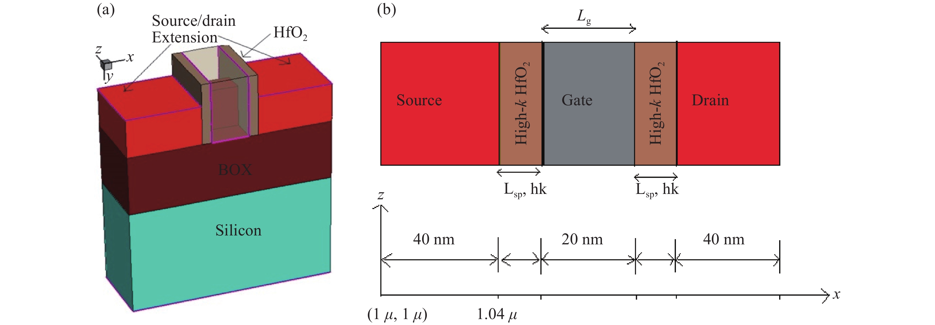
Fig. 1.
(Color online) (a) Symmetrical high-k spacer SOI FinFET (Device-D1). (b) Cross-section view of Device-D1.
SEMICONDUCTOR PHYSICS
Corresponding author: Neeraj Jain, E-mail: erneerajjain@gmail.com, balwinderraj@gmail.com
Abstract: Continued scaling of CMOS technology to achieve high performance and low power consumption of semiconductor devices in the complex integrated circuits faces the degradation in terms of electrostatic integrity, short channel effects (SCEs), leakage currents, device variability and reliability etc. Nowadays, multigate structure has become the promising candidate to overcome these problems. SOI FinFET is one of the best multigate structures that has gained importance in all electronic design automation (EDA) industries due to its improved short channel effects (SCEs), because of its more effective gate-controlling capabilities. In this paper, our aim is to explore the sensitivity of underlap spacer region variation on the performance of SOI FinFET at 20 nm channel length. Electric field modulation is analyzed with spacer length variation and electrostatic performance is evaluated in terms of performance parameter like electron mobility, electric field, electric potential, sub-threshold slope (SS), ON current (Ion), OFF current (Ioff) and Ion/Ioff ratio. The potential benefits of SOI FinFET at drain-to-source voltage, VDS = 0.05 V and VDS = 0.7 V towards analog and RF design is also evaluated in terms of intrinsic gain (AV), output conductance (gd), trans-conductance (gm), gate capacitance (Cgg), and cut-off frequency (fT = gm/2πCgg) with spacer region variations.
Keywords: SOI FinFET, SCEs, underlap region, DIBL, analog and RF performance
| [1] |
Kim Y B. Challenges for nanoscale MOSFETs and emerging nanoelectronics. Trans Electr Electron Mater, 2010, 11(3): 93 doi: 10.4313/TEEM.2010.11.3.093
|
| [2] |
Hisamoto D, Lee W C, Kedzierski J, et al. FinFET-A self-aligned double-gate MOSFET scalable to 20 nm. IEEE Trans Electron Devices, 2000, 47(12): 2320 doi: 10.1109/16.887014
|
| [3] |
Nowak E J, Aller I, Ludwig T, et al. Turning silicon on its edge double gate CMOS/FinFET technology. Circuits Devices Mag IEEE, 2004, 20(1): 20 doi: 10.1109/MCD.2004.1263404
|
| [4] |
Pal P K, Kaushik B K, Dasgupta S. High-performance and robust SRAM cell based on asymmetric dual-k spacer FinFETs. IEEE Trans Electron Devices, 2013, 60(10): 3371 doi: 10.1109/TED.2013.2278201
|
| [5] |
Pal P K, Kaushik B K, Dasgupta S. Investigation of symmetric dual- kspacer trigate FinFETs from delay perspective. IEEE Trans Electron Devices, 2014, 61(11): 3579 doi: 10.1109/TED.2014.2351616
|
| [6] |
Pavanello M A, Martino J A, Simoen E, et al. Analog performance of standard and strained triple-gate silicon-on-insulator nFinFETs. Solid State Electron, 2008, 52(12): 1904 doi: 10.1016/j.sse.2008.06.049
|
| [7] |
Kranti A, Armstrong G A. Design and optimization of FinFETs for ultra-low-voltage analog applications. IEEE Trans Electron Devices,2007, 54(12): 3308 doi: 10.1109/TED.2007.908596
|
| [8] |
Sohn C W, Kang C Y, Baek R H, et al. Device design guidelines for nanoscale FinFETs in RF/analog applications. Electron Device Lett, 2012, 33(9): 1234 doi: 10.1109/LED.2012.2204853
|
| [9] |
Kranti A, Armstrong G A. Source/drain extension region engineering in nanoscale double gate SOI MOSFETs: novel design methodology for low-voltage analog applications. Microelectron Eng, 2007, 84(12): 2775 doi: 10.1016/j.mee.2007.01.157
|
| [10] |
Virani H G, Adari R B R, Kottantharayil A. Dual-k spacer device architecture for the improvement of performance of silicon n-channel tunnel FETs. IEEE Trans Electron Devices, 2010, 57(10): 2410 doi: 10.1109/TED.2010.2057195
|
| [11] |
Park J T, Colinge J P, Diaz C H. Pi-gate SOI MOSFET. IEEE Electron Device Lett, 2001, 22(8): 405 doi: 10.1109/55.936358
|
| [12] |
Colinge J P, Chandrakasan A. FinFETs and other multi-gate transistors. Springer, 2008
|
| [13] |
Vishvakarma S K, Agrawal V, Raj B, et al. Two dimensional analytical potential modeling of nanoscale symmetric double gate (SDG) MOSFET with ultra thin body (UTB). J Comput Theor Nanosci, 2007, 4(6): 1144 doi: 10.1166/jctn.2007.2390
|
| [14] |
Raj B, Saxena A K, Dasgupta S. Analytical modeling for the estimation of leakage current and subthreshold swing factor of nanoscale double gate FinFET device. Microelectron Int, 2009, 26(1): 53 doi: 10.1108/13565360910923188
|
| [15] |
Sharma V K, Pattanaik M, Raj B. INDEP approach for leakage reduction in nanoscale CMOS circuits. Int J Electron, 2015, 102(2): 200 doi: 10.1080/00207217.2014.896042
|
| [16] |
Raj B, Saxena A K, Dasgupta S. A compact drain current and threshold voltage quantum mechanical analytical modeling for FinFETs. J Nanoelectron Optoelectron, 2008,3(2):163 doi: 10.1166/jno.2008.209
|
| [17] |
Raj B. Quantum mechanical potential modeling of FinFET. In: Toward Quantum FinFET. Springer, 2013
|
| [18] |
Singh N, Lim F Y, Fang W W, et al. Ultra-narrow silicon nanowire gate-all-around CMOS devices: Impact of diameter, channel-orientation and low temperature on device performance. Technical Digest–International Electron Devices Meeting, 2006
|
| [19] |
Sharma V K, Pattanaik M, Raj B. PVT variations aware low leakage INDEP approach for nanoscale CMOS circuits. Microelectron Reliab, 2014, 54(1): 90 doi: 10.1016/j.microrel.2013.09.018
|
| [20] |
Nandi A, Saxena A K, Dasgupta S. Impact of dual-k spacer on analog performance of underlap FinFET. Microelectron J, 2012, 43(11): 883 doi: 10.1016/j.mejo.2012.06.001
|
| [21] |
Sachid A B, Manoj C R, Sharma D K, et al. Gate fringe-induced barrier lowering in underlap FinFET structures and its optimization. IEEE Electron Device Lett, 2008, 29(1): 128 doi: 10.1109/LED.2007.911974
|
| [22] |
Kranti A, Chung T M, Raskin J P. Analysis of static and dynamic performance of short-channel double-gate silicon-on-insulator metal–oxide–semiconductor field-effect transistors for improved cutoff frequency. Jpn J Appl Phy, 2005, 44(4S): 2340
|
| [23] |
Lim T C,Armstrong G A. The impact of the intrinsic and extrinsic resistances of double gate SOI on RF performance. Solid State Electron, 2006, 50(5): 774 doi: 10.1016/j.sse.2006.04.010
|
| [24] |
Liang X, Taur Y. A 2-D analytical solution for SCEs in DG MOSFETs. IEEE Trans Electron Devices, 2004, 51(9): 1385 doi: 10.1109/TED.2004.832707
|
| [25] |
Taur Y, Liang X, Wang W, et al. A continuous, analytic drain-current model for DG MOSFETs. IEEE Electron Device Lett, 2004, 25(2): 107 doi: 10.1109/LED.2003.822661
|
| [26] |
Vandooren A, Cristoloveanu S, Colinge J P. Hall mobility measurement in double-gate SOI MOSFETs SOI Conference. IEEE International (IEEE), 2000: 118
|
| [27] |
Khan H R, Mamaluy D, Vasileska D. Approaching optimal characteristics of 10-nm high-performance devices: A quantum transport simulation study of Si FinFET. IEEE Trans Electron Devices, 2008, 55(3): 743 doi: 10.1109/TED.2007.915387
|
| [28] |
Uchida K, Koga J, Takagi S. Experimental study on carrier transport mechanisms in double-and single-gate ultrathin-body MOSFETs-Coulomb scattering, volume inversion, and d TSOI-induced scattering. IEEE International Electron Devices Meeting, 2003: 33
|
| [29] |
Dixit A, Kottantharayil A, Collaert N, et al. Analysis of the parasitic S/D resistance in multiple-gate FETs. IEEE Trans Electron Devices, 2005, 52(6): 1132 doi: 10.1109/TED.2005.848098
|
| [30] |
Kedzierski J, Ieong M, Nowak E, et al. Extension and source/drain design for high-performance FinFET devices. IEEE Trans Electron Devices, 2003, (4): 952
|
| [31] |
Tekleab D, Samavedam S , Zeitzoff P. Modeling and analysis of parasitic resistance in double-gate FinFETs. IEEE Trans Electron Devices, 2009, 56(10): 2291 doi: 10.1109/TED.2009.2028377
|
| [32] |
Matsukawa T, Endo K, Ishikawa Y, et al. Impact of extension and source/drain resistance on FinFET performance. IEEE International SOI Conference, 2008: 159
|
| [33] |
Rösner W, Landgraf E, Kretz J, et al. Nanoscale FinFETs for low power applications. Solid State Electron, 2004, 48(10): 1819
|
| [34] |
Kranti A , Armstrong G A. Source/drain extension region engineering in FinFETs for low-voltage analog applications. IEEE Electron Device Lett, 2007, 28(2): 139 doi: 10.1109/LED.2006.889239
|
| [35] |
Yu B, Y Bin, Chang L C L, et al. FinFET scaling to 10 nm gate length. Dig Int Electron Devices Meet, 2002: 251
|
| [36] |
Patil G C, Qureshi S. Engineering spacers in dopant-segregated Schottky barrier SOI MOSFET for nanoscale CMOS logic circuits. Semicond Sci Technol, 2012, 27(4): 045004 doi: 10.1088/0268-1242/27/4/045004
|
| [37] |
Pal P K, Kaushik B K, Dasgupta S. Asymmetric Dual-Spacer Trigate FinFET Device-Circuit Codesign and Its Variability Analysis. IEEE Trans. Electron Devices, 2015, 62(4): 1105 doi: 10.1109/TED.2015.2400053
|
| [38] |
Goel A, Gupta S K, Roy K. Asymmetric drain spacer extension (ADSE) FinFETs for low-power and robust SRAMs. IEEE Trans Electron Devices, 2011, 58(2): 296 doi: 10.1109/TED.2010.2090421
|
| [39] |
Magnone P, Mercha A, Subramanian V, et al. Matching performance of FinFET devices with fin widths down to 10 nm. IEEE Electron Device Lett, 2009, 30(12): 1374 doi: 10.1109/LED.2009.2034117
|
| [40] |
Nowak EJ. Maintaining the benefits of CMOS scaling when scaling bogs down. IBM J Res Dev, 2002, 46(2.3): 169 doi: 10.1147/rd.462.0169
|
| [41] |
http://www.synopsys.com/. Sentaurus TCAD User’s Manual. In: Synopsys Sentaurus Device. 2009
|
| [42] |
Pradhan K P, Mohapatra S K, Sahu P K, et al. Impact of high-k gate dielectric on analog and RF performance of nanoscale DG-MOSFET. Microelectronics J, 2014, 45(2): 144 doi: 10.1016/j.mejo.2013.11.016
|
| [43] |
Ho B, Sun X, Shin C, et al. Design optimization of multigate bulk MOSFETs. IEEE Trans Electron Devices, 2013, 60(1): 28 doi: 10.1109/TED.2012.2224870
|
| [44] |
De Andrade M G C, Martino J A, Aoulaiche M, et al. Behavior of triple-gate Bulk FinFETs with and without DTMOS operation. Solid-State Electron, 2012, 71: 63 doi: 10.1016/j.sse.2011.10.022
|
| [45] |
ITRS. International technology roadmap for semiconductors, 2013
|
| [46] |
Canali C, Majni G, Minder R, et al. Electron and hole drift velocity measurements in silicon and their empirical relation to electric field and temperature. IEEE Trans Electron Devices, 1975, 22(11): 1045 doi: 10.1109/T-ED.1975.18267
|
| [47] |
Lombardi C, Manzini S, Saporito A, et al. A physically based mobility model for numerical simulation of nonplanar devices. IEEE Trans Comput Des Integr Circuits Syst, 1988, 7(11): 1164 doi: 10.1109/43.9186
|
| [48] |
Shockley W, Read W T. Statistics of the recombination of holes and electrons. Phys Rev, 1952, 87(46): 835
|
| [49] |
Hall R N. Electron-hole recombination in germanium. Phys Rev, 1952, 87(2): 387
|
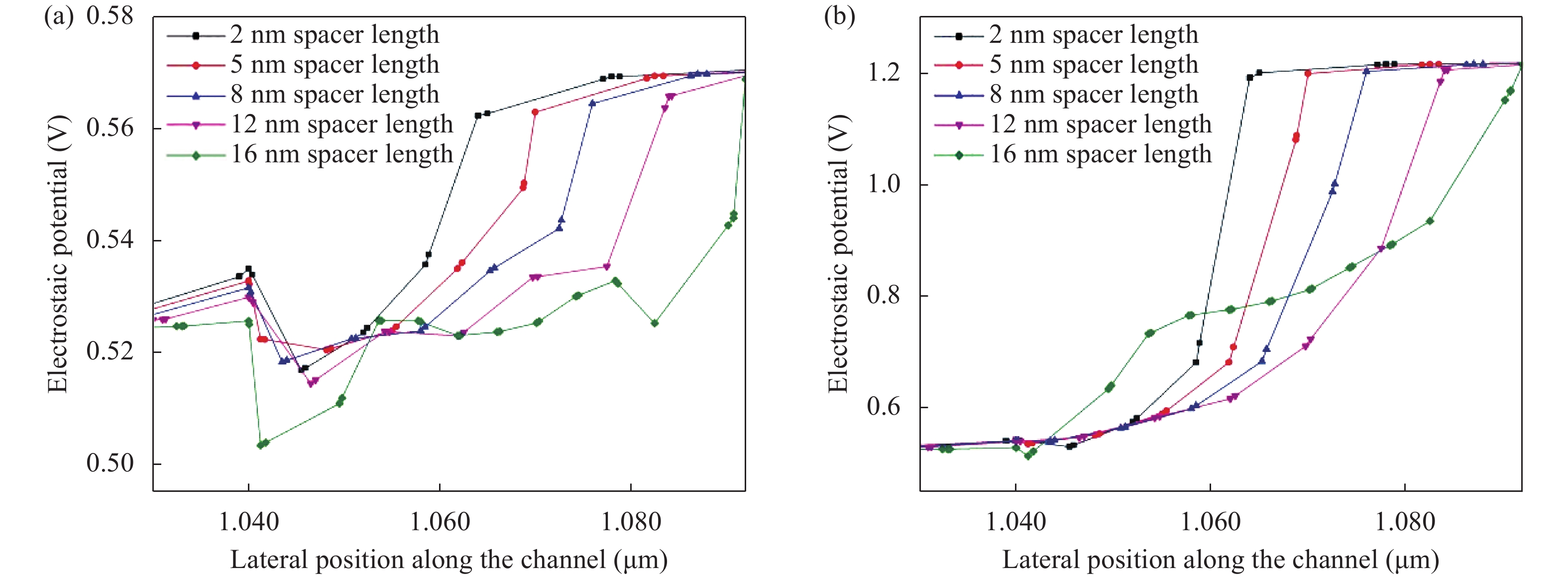
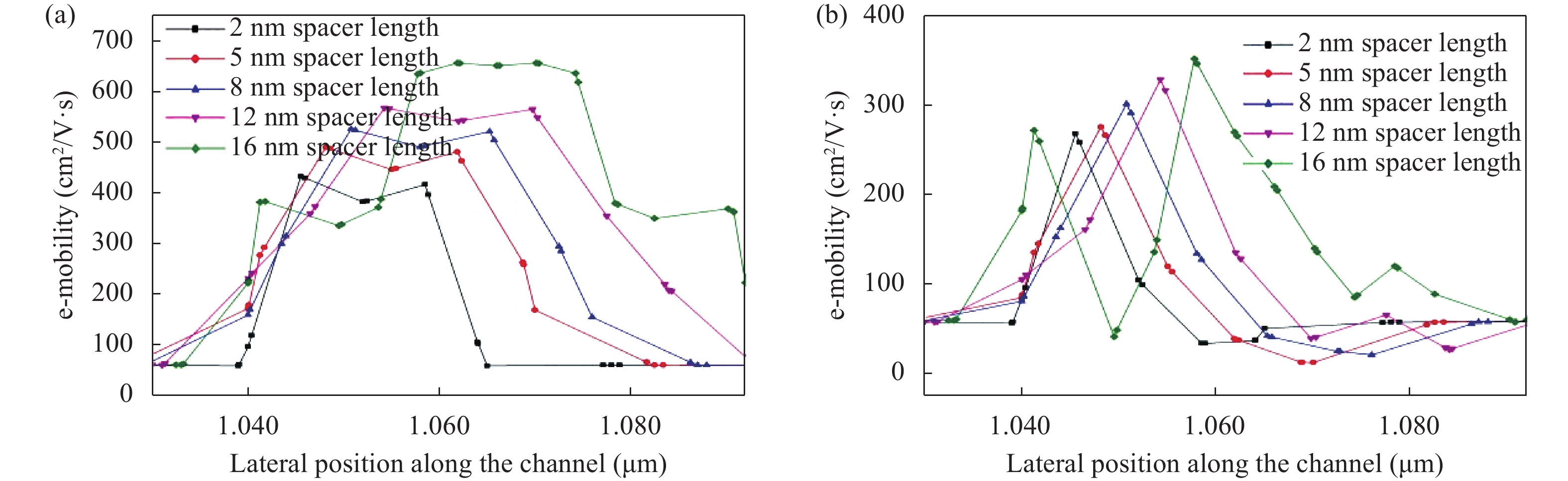
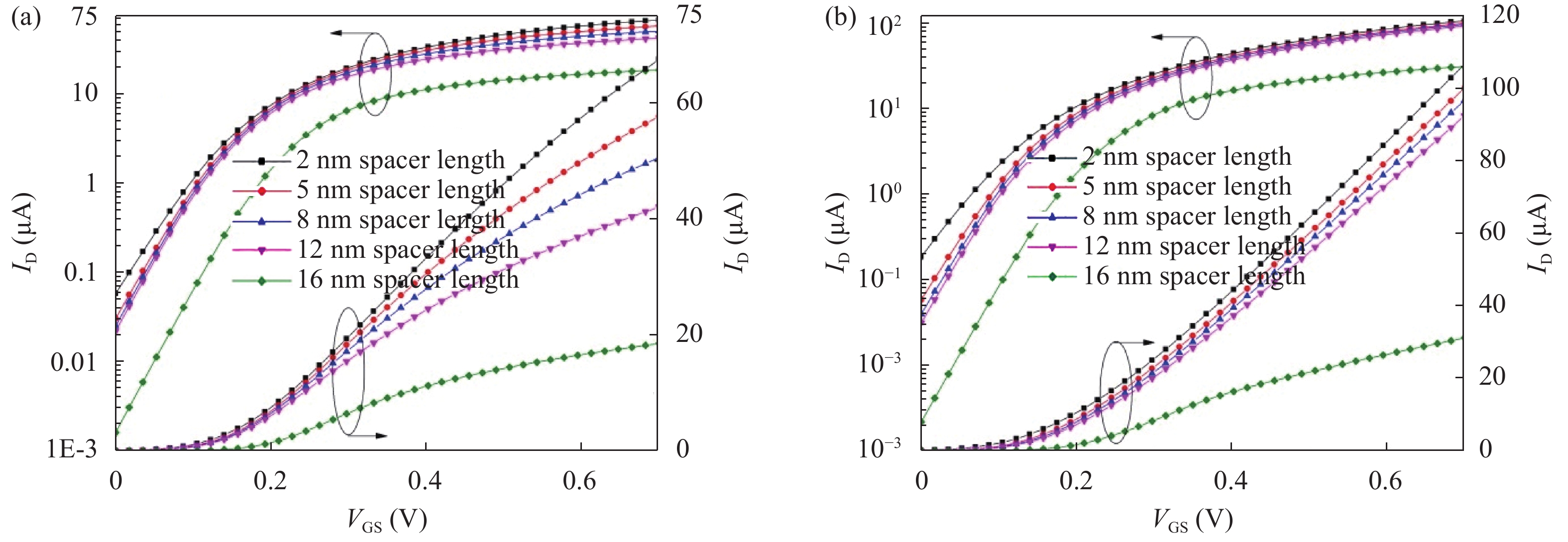
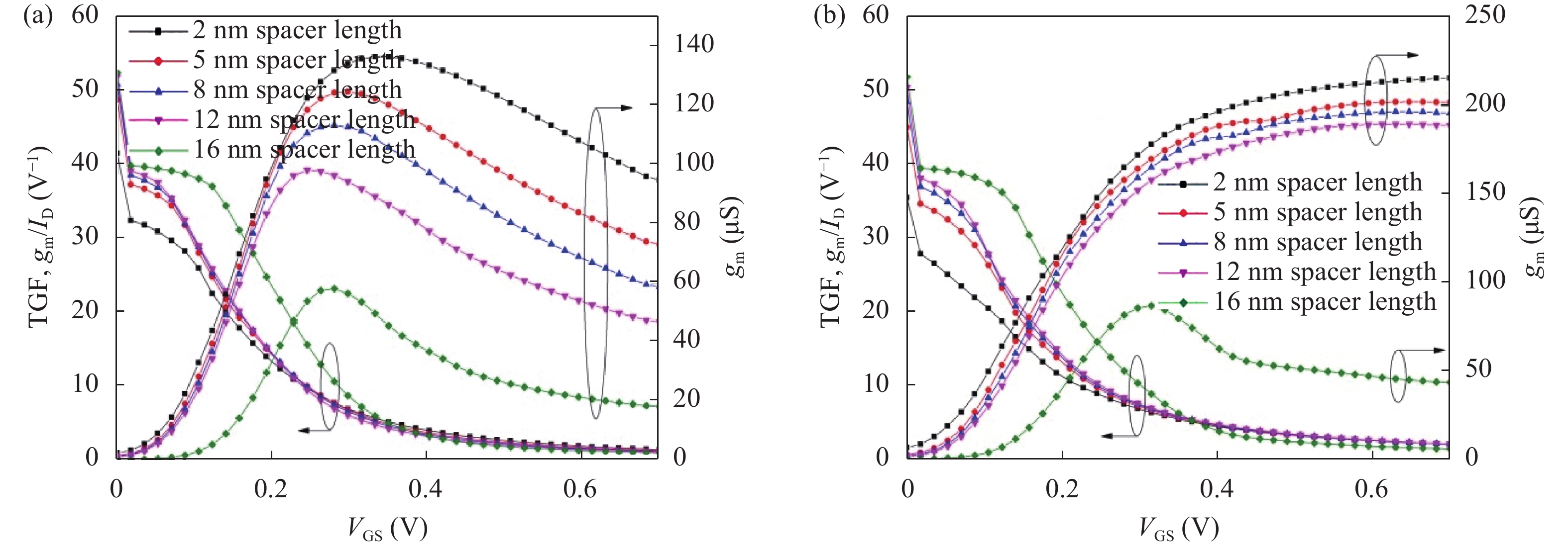
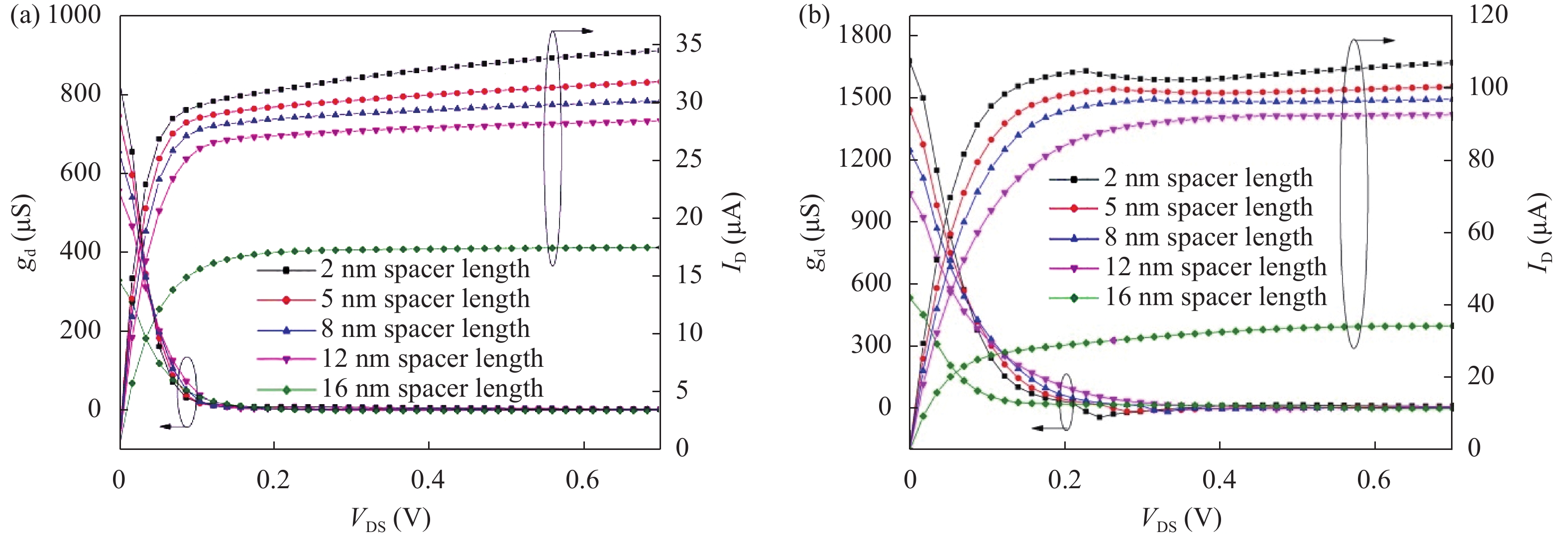
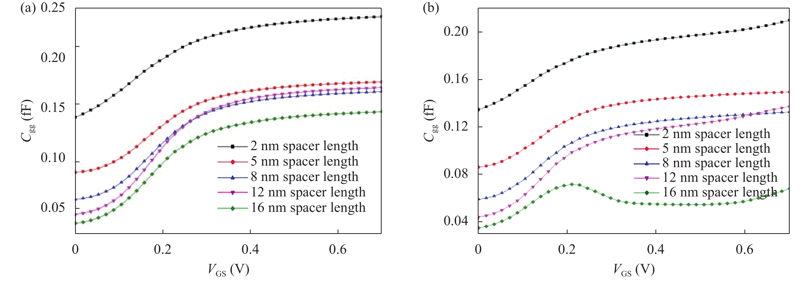
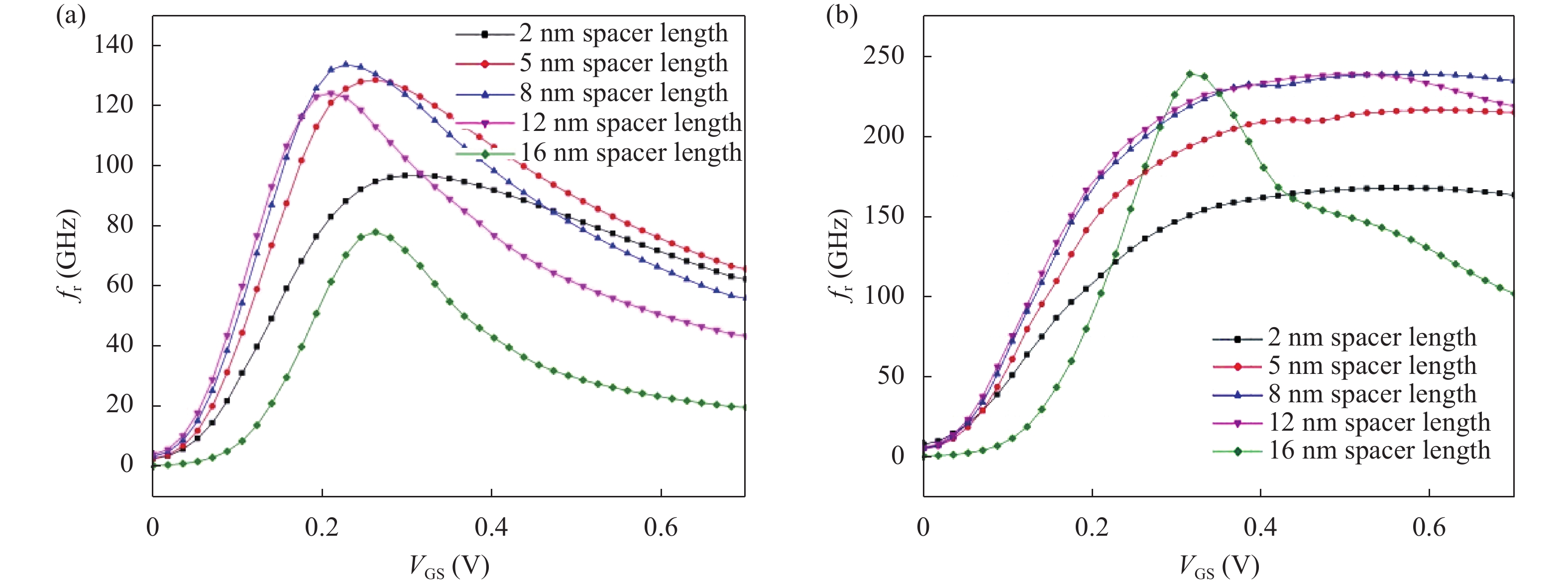
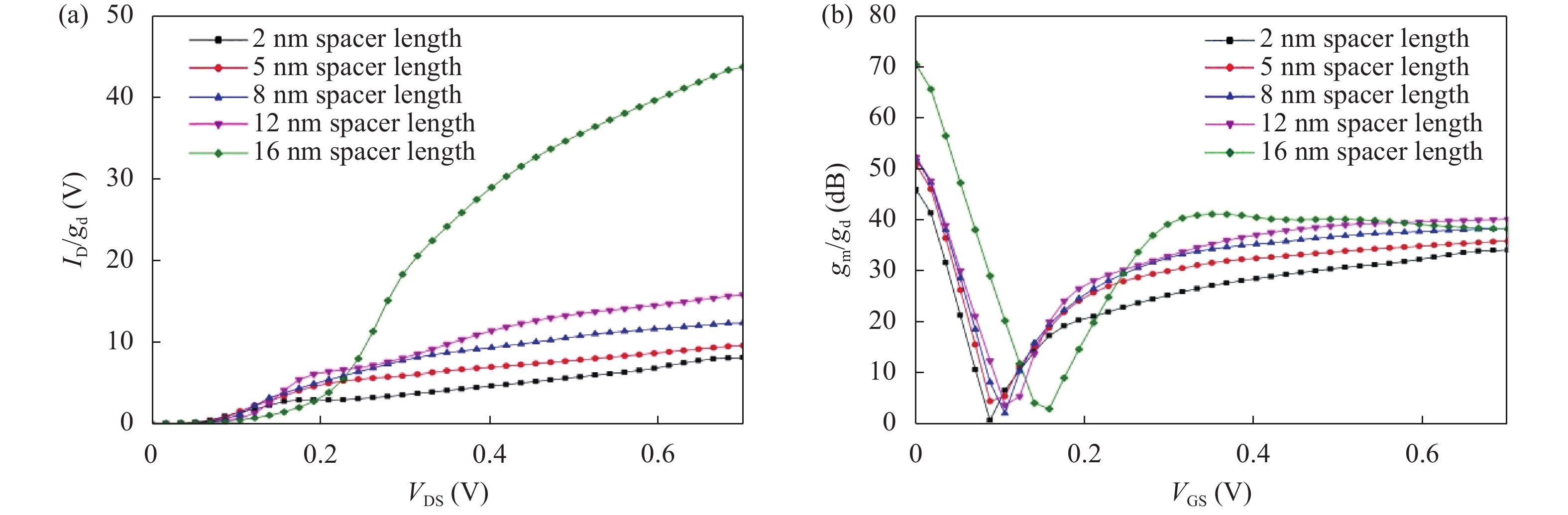
Table 1. Dimensional values used for simulation in this paper.
| Parameter | Description | Device-D1 | ||
| WFin | Fin width | 10 nm | ||
| HFin | Fin height | 26 nm | ||
| Lg | Gate channel length | 20 nm | ||
| tox | Oxide thickness | 0.9 nm | ||
| BOX | Thickness of buried oxide | 40 nm | ||
| Lsp, hk | High-k (HfO2, k = 22) spacer length under source/drain side | 2–16 nm | ||
| Ws/d | Source/drain width | 40 nm |
 DownLoad: CSV
Table 2. Simulated results at different spacer length for SOI FinFET at VDS = 0.05 V.
| Device spacer
region, Lsp, hk |
SS (mV/decade) | Ion (μA) | Ioff (nA) | Ion/Ioff | TGF (V−1) | gm (S) | gd (S) | Cgg (fF) | fT (GHz) | Gain, AV (gm/gd) (dB) |
| 2 nm | 74.38 | 67.49 | 57.99 | 1163.8 | 30.8 | 1.05 × 10⁻⁴ | 4.99 × 10⁻⁷ | 0.202 | 83.1 | 46.46 |
| 5 nm | 66.41 | 57.67 | 30.45 | 1893.9 | 35.7 | 9.28 × 10⁻⁵ | 1.23 × 10⁻⁷ | 0.131 | 113 | 57.55 |
| 8 nm | 64.87 | 50.56 | 25.13 | 2011.9 | 36.8 | 8.91 × 10⁻⁵ | 1.43 × 10⁻⁷ | 0.113 | 126 | 55.89 |
| 12 nm | 64.15 | 42.04 | 22.02 | 1909.2 | 37.5 | 8.31 × 10⁻⁵ | 8.57 × 10⁻⁸ | 0.108 | 123 | 59.73 |
| 16 nm | 64.91 | 18.54 | 1.61 | 11515.5 | 39.4 | 5.37 × 10⁻⁵ | 5.71 × 10⁻⁸ | 0.112 | 76.3 | 59.47 |
DownLoad: CSV
Table 3. Simulated results at different spacer length for SOI FinFET at VDS = 0.7 V.
| Device spacer region, Lsp, hk | SS (mV/decade) | Ion (μA) | Ioff (nA) | Ion/Ioff | TGF (V−1) | gm (S) | gd (S) | Cgg (fF) | fT (GHz) | Gain, AV (gm/gd)(dB) |
| 2 nm | 83.53 | 106.80 | 185.85 | 574.7 | 25 | 2.15 × 10⁻⁴ | 1.14 × 10⁻⁵ | 0.210 | 163 | 25.5 |
| 5 nm | 69.89 | 100.23 | 58.56 | 1711.6 | 32.5 | 2.02 × 10⁻⁴ | 5.54 × 10⁻⁶ | 0.150 | 215 | 31.24 |
| 8 nm | 66.62 | 96.80 | 39.83 | 2430.3 | 34.9 | 1.96 × 10⁻⁴ | 4.14 × 10⁻⁶ | 0.133 | 235 | 33.50 |
| 12 nm | 65.11 | 92.56 | 31.36 | 2951.5 | 36.1 | 1.89 × 10⁻⁴ | 2.25 × 10⁻⁶ | 0.137 | 219 | 38.48 |
| 16 nm | 65.12 | 31.23 | 2.19 | 14260.3 | 39.3 | 4.35 × 10⁻⁵ | 7.30 × 10⁻⁷ | 0.681 | 102 | 35.50 |
DownLoad: CSV
Table 4. Analog performance at different spacer length for SOI FinFET at VDS = VDD/2 = 0.35 V.
| Device spacer region, Lsp, hk | gm (S) | gd (S) | gm/gd (dB) | VEA (V) | TGF (V−1) | ||
| 2 nm | 2.02 × 10⁻⁴ | 8.03 × 10⁻⁶ | 28.03 | 4.01 | 25 | ||
| 5 nm | 1.99 × 10⁻⁴ | 4.72 × 10⁻⁶ | 32.50 | 6.45 | 32.5 | ||
| 8 nm | 1.96 × 10⁻⁴ | 3.37 × 10⁻⁶ | 35.29 | 8.67 | 34.9 | ||
| 12 nm | 1.85 × 10⁻⁴ | 2.86 × 10⁻⁶ | 36.21 | 9.70 | 36.1 | ||
| 16 nm | 4.39 × 10⁻⁵ | 7.18 × 10⁻⁷ | 35.72 | 24.15 | 39.3 |
DownLoad: CSV
| [1] |
Kim Y B. Challenges for nanoscale MOSFETs and emerging nanoelectronics. Trans Electr Electron Mater, 2010, 11(3): 93 doi: 10.4313/TEEM.2010.11.3.093
|
| [2] |
Hisamoto D, Lee W C, Kedzierski J, et al. FinFET-A self-aligned double-gate MOSFET scalable to 20 nm. IEEE Trans Electron Devices, 2000, 47(12): 2320 doi: 10.1109/16.887014
|
| [3] |
Nowak E J, Aller I, Ludwig T, et al. Turning silicon on its edge double gate CMOS/FinFET technology. Circuits Devices Mag IEEE, 2004, 20(1): 20 doi: 10.1109/MCD.2004.1263404
|
| [4] |
Pal P K, Kaushik B K, Dasgupta S. High-performance and robust SRAM cell based on asymmetric dual-k spacer FinFETs. IEEE Trans Electron Devices, 2013, 60(10): 3371 doi: 10.1109/TED.2013.2278201
|
| [5] |
Pal P K, Kaushik B K, Dasgupta S. Investigation of symmetric dual- kspacer trigate FinFETs from delay perspective. IEEE Trans Electron Devices, 2014, 61(11): 3579 doi: 10.1109/TED.2014.2351616
|
| [6] |
Pavanello M A, Martino J A, Simoen E, et al. Analog performance of standard and strained triple-gate silicon-on-insulator nFinFETs. Solid State Electron, 2008, 52(12): 1904 doi: 10.1016/j.sse.2008.06.049
|
| [7] |
Kranti A, Armstrong G A. Design and optimization of FinFETs for ultra-low-voltage analog applications. IEEE Trans Electron Devices,2007, 54(12): 3308 doi: 10.1109/TED.2007.908596
|
| [8] |
Sohn C W, Kang C Y, Baek R H, et al. Device design guidelines for nanoscale FinFETs in RF/analog applications. Electron Device Lett, 2012, 33(9): 1234 doi: 10.1109/LED.2012.2204853
|
| [9] |
Kranti A, Armstrong G A. Source/drain extension region engineering in nanoscale double gate SOI MOSFETs: novel design methodology for low-voltage analog applications. Microelectron Eng, 2007, 84(12): 2775 doi: 10.1016/j.mee.2007.01.157
|
| [10] |
Virani H G, Adari R B R, Kottantharayil A. Dual-k spacer device architecture for the improvement of performance of silicon n-channel tunnel FETs. IEEE Trans Electron Devices, 2010, 57(10): 2410 doi: 10.1109/TED.2010.2057195
|
| [11] |
Park J T, Colinge J P, Diaz C H. Pi-gate SOI MOSFET. IEEE Electron Device Lett, 2001, 22(8): 405 doi: 10.1109/55.936358
|
| [12] |
Colinge J P, Chandrakasan A. FinFETs and other multi-gate transistors. Springer, 2008
|
| [13] |
Vishvakarma S K, Agrawal V, Raj B, et al. Two dimensional analytical potential modeling of nanoscale symmetric double gate (SDG) MOSFET with ultra thin body (UTB). J Comput Theor Nanosci, 2007, 4(6): 1144 doi: 10.1166/jctn.2007.2390
|
| [14] |
Raj B, Saxena A K, Dasgupta S. Analytical modeling for the estimation of leakage current and subthreshold swing factor of nanoscale double gate FinFET device. Microelectron Int, 2009, 26(1): 53 doi: 10.1108/13565360910923188
|
| [15] |
Sharma V K, Pattanaik M, Raj B. INDEP approach for leakage reduction in nanoscale CMOS circuits. Int J Electron, 2015, 102(2): 200 doi: 10.1080/00207217.2014.896042
|
| [16] |
Raj B, Saxena A K, Dasgupta S. A compact drain current and threshold voltage quantum mechanical analytical modeling for FinFETs. J Nanoelectron Optoelectron, 2008,3(2):163 doi: 10.1166/jno.2008.209
|
| [17] |
Raj B. Quantum mechanical potential modeling of FinFET. In: Toward Quantum FinFET. Springer, 2013
|
| [18] |
Singh N, Lim F Y, Fang W W, et al. Ultra-narrow silicon nanowire gate-all-around CMOS devices: Impact of diameter, channel-orientation and low temperature on device performance. Technical Digest–International Electron Devices Meeting, 2006
|
| [19] |
Sharma V K, Pattanaik M, Raj B. PVT variations aware low leakage INDEP approach for nanoscale CMOS circuits. Microelectron Reliab, 2014, 54(1): 90 doi: 10.1016/j.microrel.2013.09.018
|
| [20] |
Nandi A, Saxena A K, Dasgupta S. Impact of dual-k spacer on analog performance of underlap FinFET. Microelectron J, 2012, 43(11): 883 doi: 10.1016/j.mejo.2012.06.001
|
| [21] |
Sachid A B, Manoj C R, Sharma D K, et al. Gate fringe-induced barrier lowering in underlap FinFET structures and its optimization. IEEE Electron Device Lett, 2008, 29(1): 128 doi: 10.1109/LED.2007.911974
|
| [22] |
Kranti A, Chung T M, Raskin J P. Analysis of static and dynamic performance of short-channel double-gate silicon-on-insulator metal–oxide–semiconductor field-effect transistors for improved cutoff frequency. Jpn J Appl Phy, 2005, 44(4S): 2340
|
| [23] |
Lim T C,Armstrong G A. The impact of the intrinsic and extrinsic resistances of double gate SOI on RF performance. Solid State Electron, 2006, 50(5): 774 doi: 10.1016/j.sse.2006.04.010
|
| [24] |
Liang X, Taur Y. A 2-D analytical solution for SCEs in DG MOSFETs. IEEE Trans Electron Devices, 2004, 51(9): 1385 doi: 10.1109/TED.2004.832707
|
| [25] |
Taur Y, Liang X, Wang W, et al. A continuous, analytic drain-current model for DG MOSFETs. IEEE Electron Device Lett, 2004, 25(2): 107 doi: 10.1109/LED.2003.822661
|
| [26] |
Vandooren A, Cristoloveanu S, Colinge J P. Hall mobility measurement in double-gate SOI MOSFETs SOI Conference. IEEE International (IEEE), 2000: 118
|
| [27] |
Khan H R, Mamaluy D, Vasileska D. Approaching optimal characteristics of 10-nm high-performance devices: A quantum transport simulation study of Si FinFET. IEEE Trans Electron Devices, 2008, 55(3): 743 doi: 10.1109/TED.2007.915387
|
| [28] |
Uchida K, Koga J, Takagi S. Experimental study on carrier transport mechanisms in double-and single-gate ultrathin-body MOSFETs-Coulomb scattering, volume inversion, and d TSOI-induced scattering. IEEE International Electron Devices Meeting, 2003: 33
|
| [29] |
Dixit A, Kottantharayil A, Collaert N, et al. Analysis of the parasitic S/D resistance in multiple-gate FETs. IEEE Trans Electron Devices, 2005, 52(6): 1132 doi: 10.1109/TED.2005.848098
|
| [30] |
Kedzierski J, Ieong M, Nowak E, et al. Extension and source/drain design for high-performance FinFET devices. IEEE Trans Electron Devices, 2003, (4): 952
|
| [31] |
Tekleab D, Samavedam S , Zeitzoff P. Modeling and analysis of parasitic resistance in double-gate FinFETs. IEEE Trans Electron Devices, 2009, 56(10): 2291 doi: 10.1109/TED.2009.2028377
|
| [32] |
Matsukawa T, Endo K, Ishikawa Y, et al. Impact of extension and source/drain resistance on FinFET performance. IEEE International SOI Conference, 2008: 159
|
| [33] |
Rösner W, Landgraf E, Kretz J, et al. Nanoscale FinFETs for low power applications. Solid State Electron, 2004, 48(10): 1819
|
| [34] |
Kranti A , Armstrong G A. Source/drain extension region engineering in FinFETs for low-voltage analog applications. IEEE Electron Device Lett, 2007, 28(2): 139 doi: 10.1109/LED.2006.889239
|
| [35] |
Yu B, Y Bin, Chang L C L, et al. FinFET scaling to 10 nm gate length. Dig Int Electron Devices Meet, 2002: 251
|
| [36] |
Patil G C, Qureshi S. Engineering spacers in dopant-segregated Schottky barrier SOI MOSFET for nanoscale CMOS logic circuits. Semicond Sci Technol, 2012, 27(4): 045004 doi: 10.1088/0268-1242/27/4/045004
|
| [37] |
Pal P K, Kaushik B K, Dasgupta S. Asymmetric Dual-Spacer Trigate FinFET Device-Circuit Codesign and Its Variability Analysis. IEEE Trans. Electron Devices, 2015, 62(4): 1105 doi: 10.1109/TED.2015.2400053
|
| [38] |
Goel A, Gupta S K, Roy K. Asymmetric drain spacer extension (ADSE) FinFETs for low-power and robust SRAMs. IEEE Trans Electron Devices, 2011, 58(2): 296 doi: 10.1109/TED.2010.2090421
|
| [39] |
Magnone P, Mercha A, Subramanian V, et al. Matching performance of FinFET devices with fin widths down to 10 nm. IEEE Electron Device Lett, 2009, 30(12): 1374 doi: 10.1109/LED.2009.2034117
|
| [40] |
Nowak EJ. Maintaining the benefits of CMOS scaling when scaling bogs down. IBM J Res Dev, 2002, 46(2.3): 169 doi: 10.1147/rd.462.0169
|
| [41] |
http://www.synopsys.com/. Sentaurus TCAD User’s Manual. In: Synopsys Sentaurus Device. 2009
|
| [42] |
Pradhan K P, Mohapatra S K, Sahu P K, et al. Impact of high-k gate dielectric on analog and RF performance of nanoscale DG-MOSFET. Microelectronics J, 2014, 45(2): 144 doi: 10.1016/j.mejo.2013.11.016
|
| [43] |
Ho B, Sun X, Shin C, et al. Design optimization of multigate bulk MOSFETs. IEEE Trans Electron Devices, 2013, 60(1): 28 doi: 10.1109/TED.2012.2224870
|
| [44] |
De Andrade M G C, Martino J A, Aoulaiche M, et al. Behavior of triple-gate Bulk FinFETs with and without DTMOS operation. Solid-State Electron, 2012, 71: 63 doi: 10.1016/j.sse.2011.10.022
|
| [45] |
ITRS. International technology roadmap for semiconductors, 2013
|
| [46] |
Canali C, Majni G, Minder R, et al. Electron and hole drift velocity measurements in silicon and their empirical relation to electric field and temperature. IEEE Trans Electron Devices, 1975, 22(11): 1045 doi: 10.1109/T-ED.1975.18267
|
| [47] |
Lombardi C, Manzini S, Saporito A, et al. A physically based mobility model for numerical simulation of nonplanar devices. IEEE Trans Comput Des Integr Circuits Syst, 1988, 7(11): 1164 doi: 10.1109/43.9186
|
| [48] |
Shockley W, Read W T. Statistics of the recombination of holes and electrons. Phys Rev, 1952, 87(46): 835
|
| [49] |
Hall R N. Electron-hole recombination in germanium. Phys Rev, 1952, 87(2): 387
|


Article views: 6061 Times PDF downloads: 115 Times Cited by: 0 Times
Received: 29 January 2017 Revised: 26 May 2017 Online: Corrected proof: 15 November 2017Accepted Manuscript: 06 December 2017Published: 01 December 2017
| Citation: |
Neeraj Jain, Balwinder Raj. Impact of underlap spacer region variation on electrostatic and analog performance of symmetrical high-k SOI FinFET at 20 nm channel length[J]. Journal of Semiconductors, 2017, 38(12): 122002. doi: 10.1088/1674-4926/38/12/122002
****
N Jain, B Raj. Impact of underlap spacer region variation on electrostatic and analog performance of symmetrical high-k SOI FinFET at 20 nm channel length[J]. J. Semicond., 2017, 38(12): 122002. doi: 10.1088/1674-4926/38/12/122002.

|
| [1] |
Kim Y B. Challenges for nanoscale MOSFETs and emerging nanoelectronics. Trans Electr Electron Mater, 2010, 11(3): 93 doi: 10.4313/TEEM.2010.11.3.093
|
| [2] |
Hisamoto D, Lee W C, Kedzierski J, et al. FinFET-A self-aligned double-gate MOSFET scalable to 20 nm. IEEE Trans Electron Devices, 2000, 47(12): 2320 doi: 10.1109/16.887014
|
| [3] |
Nowak E J, Aller I, Ludwig T, et al. Turning silicon on its edge double gate CMOS/FinFET technology. Circuits Devices Mag IEEE, 2004, 20(1): 20 doi: 10.1109/MCD.2004.1263404
|
| [4] |
Pal P K, Kaushik B K, Dasgupta S. High-performance and robust SRAM cell based on asymmetric dual-k spacer FinFETs. IEEE Trans Electron Devices, 2013, 60(10): 3371 doi: 10.1109/TED.2013.2278201
|
| [5] |
Pal P K, Kaushik B K, Dasgupta S. Investigation of symmetric dual- kspacer trigate FinFETs from delay perspective. IEEE Trans Electron Devices, 2014, 61(11): 3579 doi: 10.1109/TED.2014.2351616
|
| [6] |
Pavanello M A, Martino J A, Simoen E, et al. Analog performance of standard and strained triple-gate silicon-on-insulator nFinFETs. Solid State Electron, 2008, 52(12): 1904 doi: 10.1016/j.sse.2008.06.049
|
| [7] |
Kranti A, Armstrong G A. Design and optimization of FinFETs for ultra-low-voltage analog applications. IEEE Trans Electron Devices,2007, 54(12): 3308 doi: 10.1109/TED.2007.908596
|
| [8] |
Sohn C W, Kang C Y, Baek R H, et al. Device design guidelines for nanoscale FinFETs in RF/analog applications. Electron Device Lett, 2012, 33(9): 1234 doi: 10.1109/LED.2012.2204853
|
| [9] |
Kranti A, Armstrong G A. Source/drain extension region engineering in nanoscale double gate SOI MOSFETs: novel design methodology for low-voltage analog applications. Microelectron Eng, 2007, 84(12): 2775 doi: 10.1016/j.mee.2007.01.157
|
| [10] |
Virani H G, Adari R B R, Kottantharayil A. Dual-k spacer device architecture for the improvement of performance of silicon n-channel tunnel FETs. IEEE Trans Electron Devices, 2010, 57(10): 2410 doi: 10.1109/TED.2010.2057195
|
| [11] |
Park J T, Colinge J P, Diaz C H. Pi-gate SOI MOSFET. IEEE Electron Device Lett, 2001, 22(8): 405 doi: 10.1109/55.936358
|
| [12] |
Colinge J P, Chandrakasan A. FinFETs and other multi-gate transistors. Springer, 2008
|
| [13] |
Vishvakarma S K, Agrawal V, Raj B, et al. Two dimensional analytical potential modeling of nanoscale symmetric double gate (SDG) MOSFET with ultra thin body (UTB). J Comput Theor Nanosci, 2007, 4(6): 1144 doi: 10.1166/jctn.2007.2390
|
| [14] |
Raj B, Saxena A K, Dasgupta S. Analytical modeling for the estimation of leakage current and subthreshold swing factor of nanoscale double gate FinFET device. Microelectron Int, 2009, 26(1): 53 doi: 10.1108/13565360910923188
|
| [15] |
Sharma V K, Pattanaik M, Raj B. INDEP approach for leakage reduction in nanoscale CMOS circuits. Int J Electron, 2015, 102(2): 200 doi: 10.1080/00207217.2014.896042
|
| [16] |
Raj B, Saxena A K, Dasgupta S. A compact drain current and threshold voltage quantum mechanical analytical modeling for FinFETs. J Nanoelectron Optoelectron, 2008,3(2):163 doi: 10.1166/jno.2008.209
|
| [17] |
Raj B. Quantum mechanical potential modeling of FinFET. In: Toward Quantum FinFET. Springer, 2013
|
| [18] |
Singh N, Lim F Y, Fang W W, et al. Ultra-narrow silicon nanowire gate-all-around CMOS devices: Impact of diameter, channel-orientation and low temperature on device performance. Technical Digest–International Electron Devices Meeting, 2006
|
| [19] |
Sharma V K, Pattanaik M, Raj B. PVT variations aware low leakage INDEP approach for nanoscale CMOS circuits. Microelectron Reliab, 2014, 54(1): 90 doi: 10.1016/j.microrel.2013.09.018
|
| [20] |
Nandi A, Saxena A K, Dasgupta S. Impact of dual-k spacer on analog performance of underlap FinFET. Microelectron J, 2012, 43(11): 883 doi: 10.1016/j.mejo.2012.06.001
|
| [21] |
Sachid A B, Manoj C R, Sharma D K, et al. Gate fringe-induced barrier lowering in underlap FinFET structures and its optimization. IEEE Electron Device Lett, 2008, 29(1): 128 doi: 10.1109/LED.2007.911974
|
| [22] |
Kranti A, Chung T M, Raskin J P. Analysis of static and dynamic performance of short-channel double-gate silicon-on-insulator metal–oxide–semiconductor field-effect transistors for improved cutoff frequency. Jpn J Appl Phy, 2005, 44(4S): 2340
|
| [23] |
Lim T C,Armstrong G A. The impact of the intrinsic and extrinsic resistances of double gate SOI on RF performance. Solid State Electron, 2006, 50(5): 774 doi: 10.1016/j.sse.2006.04.010
|
| [24] |
Liang X, Taur Y. A 2-D analytical solution for SCEs in DG MOSFETs. IEEE Trans Electron Devices, 2004, 51(9): 1385 doi: 10.1109/TED.2004.832707
|
| [25] |
Taur Y, Liang X, Wang W, et al. A continuous, analytic drain-current model for DG MOSFETs. IEEE Electron Device Lett, 2004, 25(2): 107 doi: 10.1109/LED.2003.822661
|
| [26] |
Vandooren A, Cristoloveanu S, Colinge J P. Hall mobility measurement in double-gate SOI MOSFETs SOI Conference. IEEE International (IEEE), 2000: 118
|
| [27] |
Khan H R, Mamaluy D, Vasileska D. Approaching optimal characteristics of 10-nm high-performance devices: A quantum transport simulation study of Si FinFET. IEEE Trans Electron Devices, 2008, 55(3): 743 doi: 10.1109/TED.2007.915387
|
| [28] |
Uchida K, Koga J, Takagi S. Experimental study on carrier transport mechanisms in double-and single-gate ultrathin-body MOSFETs-Coulomb scattering, volume inversion, and d TSOI-induced scattering. IEEE International Electron Devices Meeting, 2003: 33
|
| [29] |
Dixit A, Kottantharayil A, Collaert N, et al. Analysis of the parasitic S/D resistance in multiple-gate FETs. IEEE Trans Electron Devices, 2005, 52(6): 1132 doi: 10.1109/TED.2005.848098
|
| [30] |
Kedzierski J, Ieong M, Nowak E, et al. Extension and source/drain design for high-performance FinFET devices. IEEE Trans Electron Devices, 2003, (4): 952
|
| [31] |
Tekleab D, Samavedam S , Zeitzoff P. Modeling and analysis of parasitic resistance in double-gate FinFETs. IEEE Trans Electron Devices, 2009, 56(10): 2291 doi: 10.1109/TED.2009.2028377
|
| [32] |
Matsukawa T, Endo K, Ishikawa Y, et al. Impact of extension and source/drain resistance on FinFET performance. IEEE International SOI Conference, 2008: 159
|
| [33] |
Rösner W, Landgraf E, Kretz J, et al. Nanoscale FinFETs for low power applications. Solid State Electron, 2004, 48(10): 1819
|
| [34] |
Kranti A , Armstrong G A. Source/drain extension region engineering in FinFETs for low-voltage analog applications. IEEE Electron Device Lett, 2007, 28(2): 139 doi: 10.1109/LED.2006.889239
|
| [35] |
Yu B, Y Bin, Chang L C L, et al. FinFET scaling to 10 nm gate length. Dig Int Electron Devices Meet, 2002: 251
|
| [36] |
Patil G C, Qureshi S. Engineering spacers in dopant-segregated Schottky barrier SOI MOSFET for nanoscale CMOS logic circuits. Semicond Sci Technol, 2012, 27(4): 045004 doi: 10.1088/0268-1242/27/4/045004
|
| [37] |
Pal P K, Kaushik B K, Dasgupta S. Asymmetric Dual-Spacer Trigate FinFET Device-Circuit Codesign and Its Variability Analysis. IEEE Trans. Electron Devices, 2015, 62(4): 1105 doi: 10.1109/TED.2015.2400053
|
| [38] |
Goel A, Gupta S K, Roy K. Asymmetric drain spacer extension (ADSE) FinFETs for low-power and robust SRAMs. IEEE Trans Electron Devices, 2011, 58(2): 296 doi: 10.1109/TED.2010.2090421
|
| [39] |
Magnone P, Mercha A, Subramanian V, et al. Matching performance of FinFET devices with fin widths down to 10 nm. IEEE Electron Device Lett, 2009, 30(12): 1374 doi: 10.1109/LED.2009.2034117
|
| [40] |
Nowak EJ. Maintaining the benefits of CMOS scaling when scaling bogs down. IBM J Res Dev, 2002, 46(2.3): 169 doi: 10.1147/rd.462.0169
|
| [41] |
http://www.synopsys.com/. Sentaurus TCAD User’s Manual. In: Synopsys Sentaurus Device. 2009
|
| [42] |
Pradhan K P, Mohapatra S K, Sahu P K, et al. Impact of high-k gate dielectric on analog and RF performance of nanoscale DG-MOSFET. Microelectronics J, 2014, 45(2): 144 doi: 10.1016/j.mejo.2013.11.016
|
| [43] |
Ho B, Sun X, Shin C, et al. Design optimization of multigate bulk MOSFETs. IEEE Trans Electron Devices, 2013, 60(1): 28 doi: 10.1109/TED.2012.2224870
|
| [44] |
De Andrade M G C, Martino J A, Aoulaiche M, et al. Behavior of triple-gate Bulk FinFETs with and without DTMOS operation. Solid-State Electron, 2012, 71: 63 doi: 10.1016/j.sse.2011.10.022
|
| [45] |
ITRS. International technology roadmap for semiconductors, 2013
|
| [46] |
Canali C, Majni G, Minder R, et al. Electron and hole drift velocity measurements in silicon and their empirical relation to electric field and temperature. IEEE Trans Electron Devices, 1975, 22(11): 1045 doi: 10.1109/T-ED.1975.18267
|
| [47] |
Lombardi C, Manzini S, Saporito A, et al. A physically based mobility model for numerical simulation of nonplanar devices. IEEE Trans Comput Des Integr Circuits Syst, 1988, 7(11): 1164 doi: 10.1109/43.9186
|
| [48] |
Shockley W, Read W T. Statistics of the recombination of holes and electrons. Phys Rev, 1952, 87(46): 835
|
| [49] |
Hall R N. Electron-hole recombination in germanium. Phys Rev, 1952, 87(2): 387
|

 WeChat ID
Journal of Semiconductors © 2017 All Rights Reserved 京ICP备05085259号-2


