


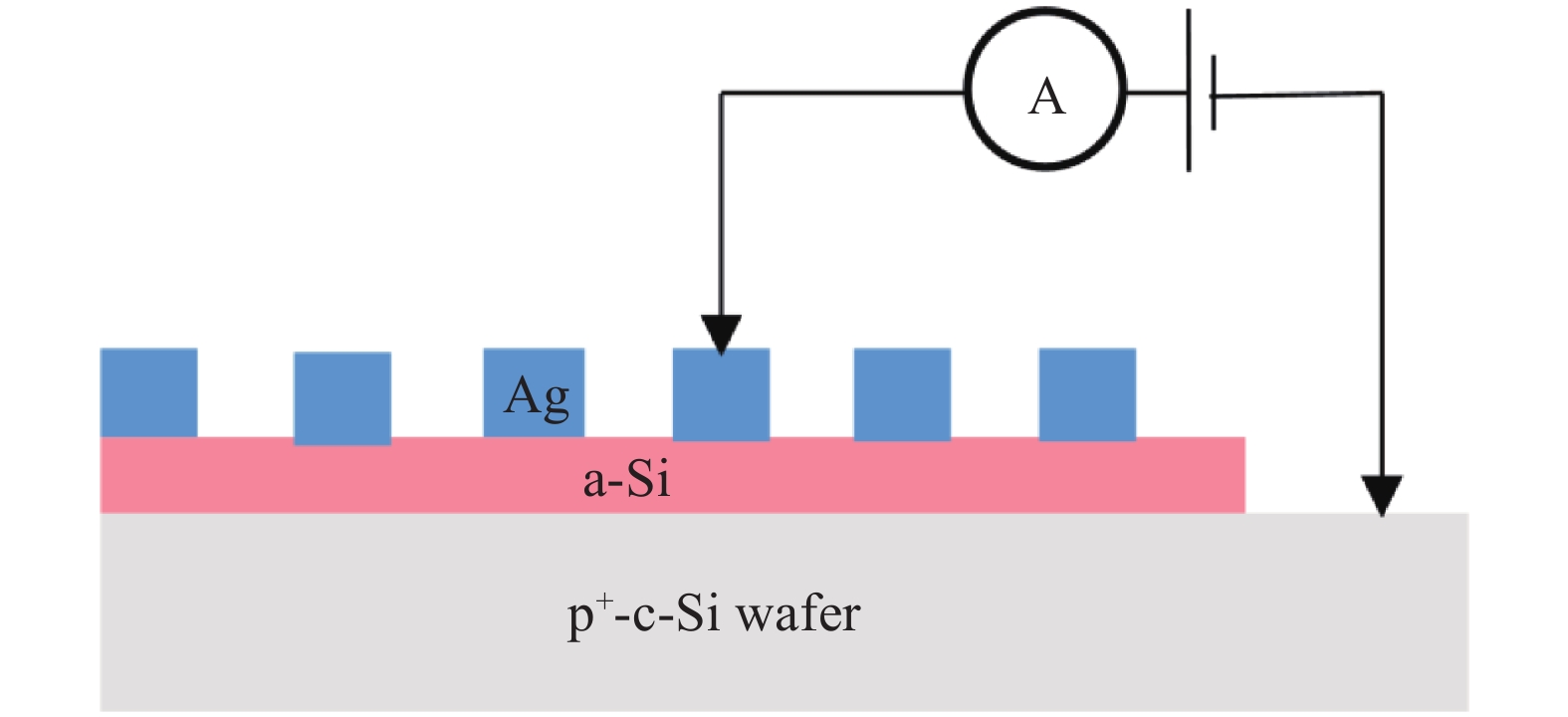
Fig. 1.
(Color online) The schematic of Ag/a-Si/p+-c-Si memory device.
SEMICONDUCTOR PHYSICS
Jiahua Zhang, Da Chen and Shihua Huang
Corresponding author: Shihua Huang, E-mail: huangshihua@zjnu.cn
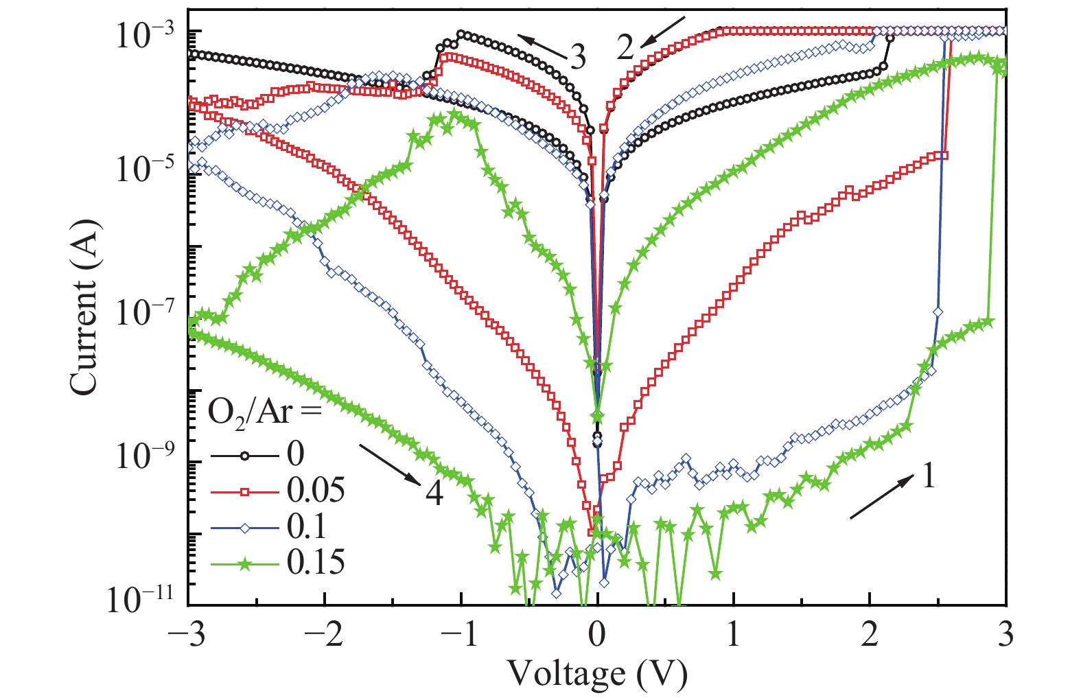
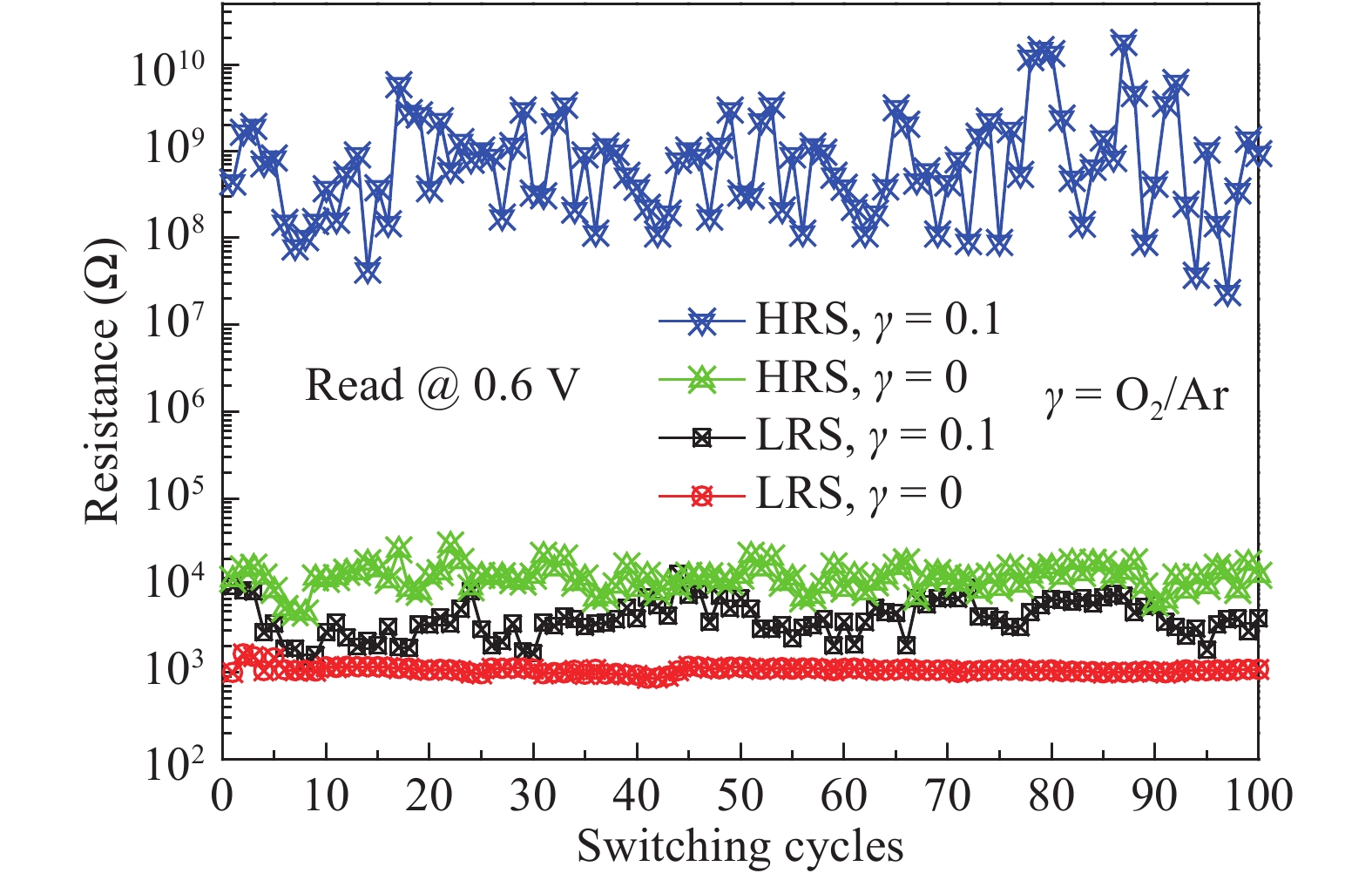
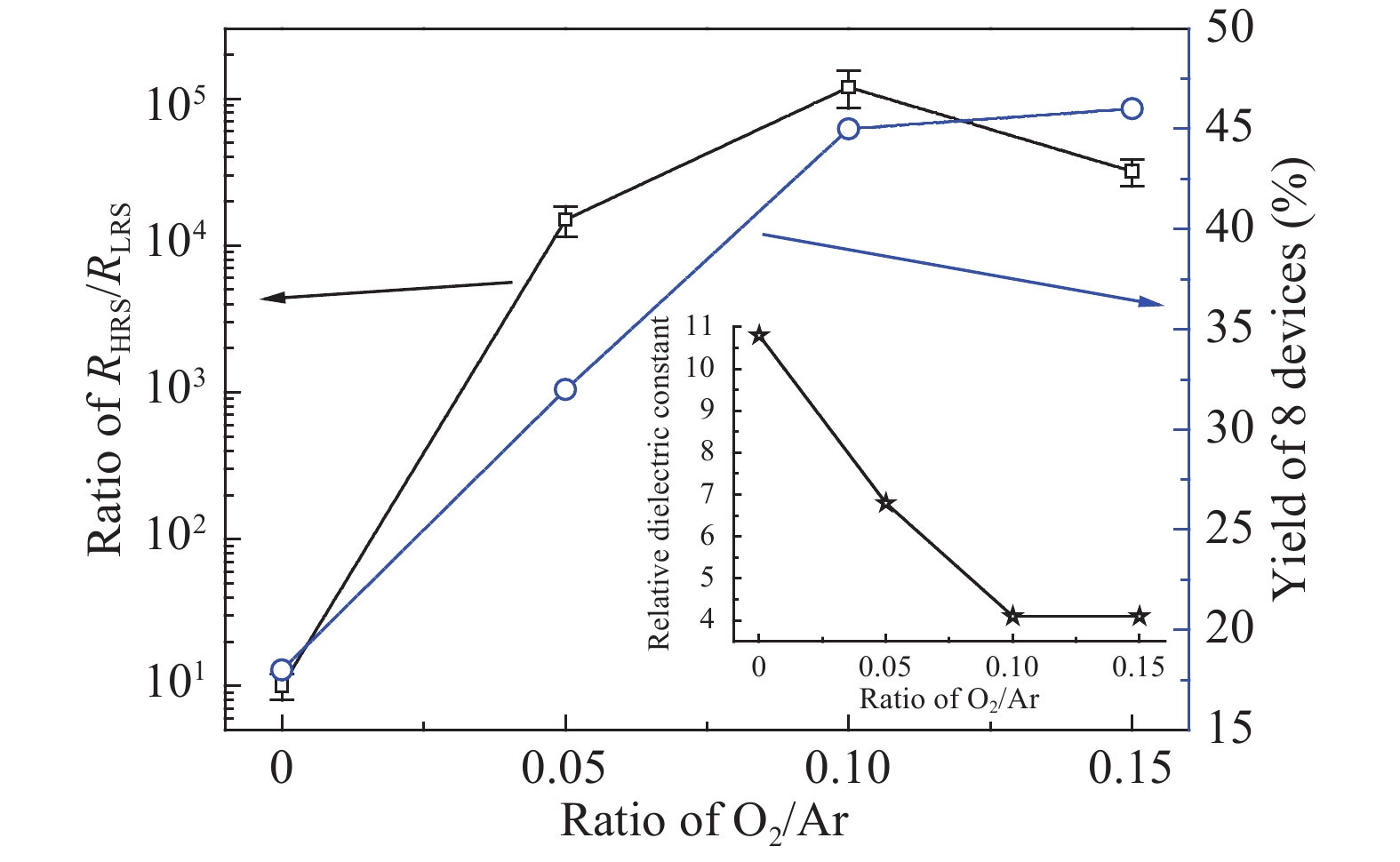
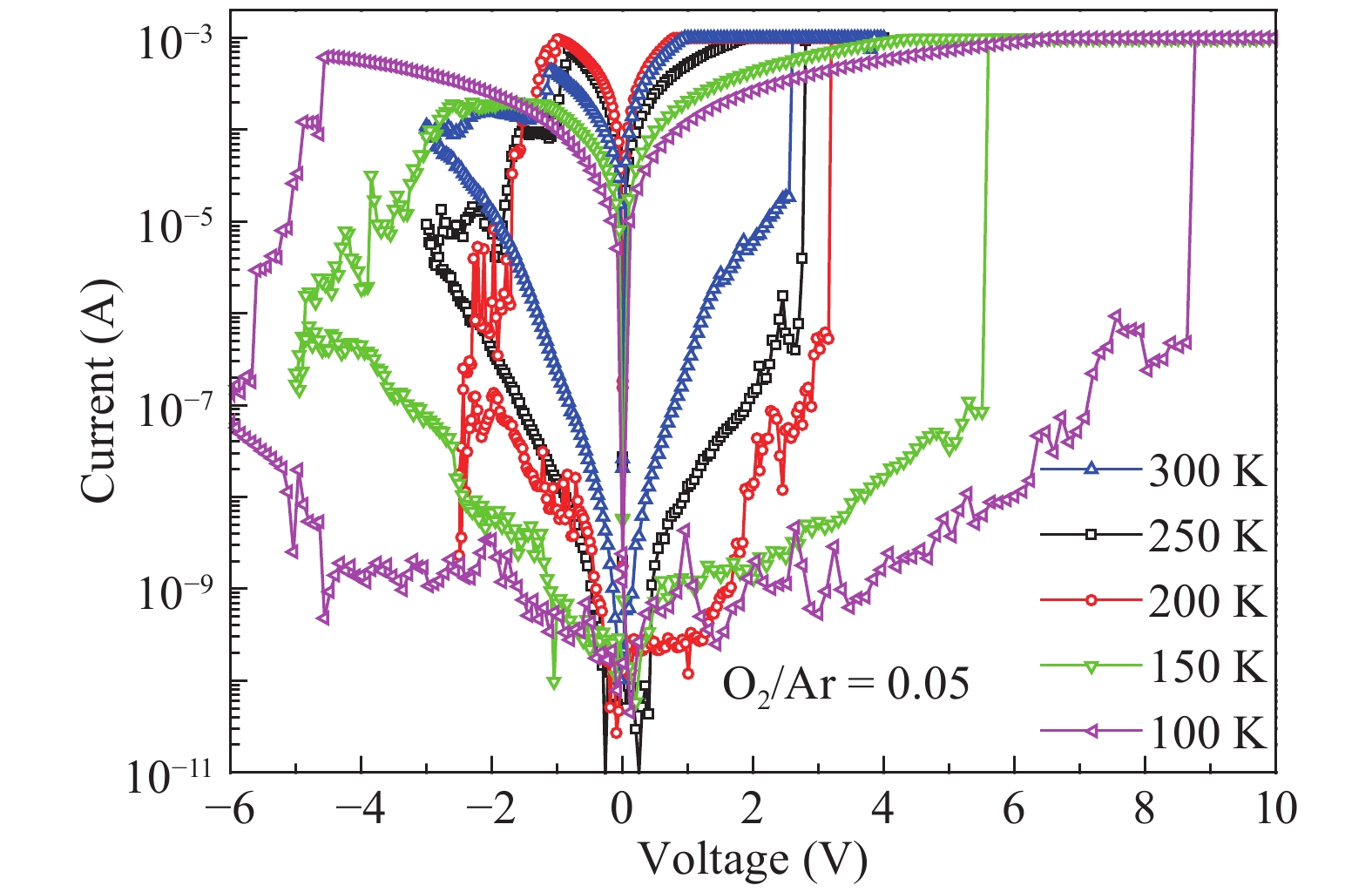
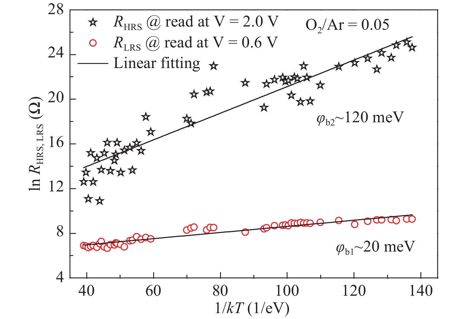
Abstract: The influence of oxygen doping on resistive-switching characteristics of Ag/a-Si/p+-c-Si device was investigated. By oxygen doping in the growth process of amorphous silicon, the device resistive-switching performances, such as the ON/OFF resistance ratios, yield and stability were improved, which may be ascribed to the significant reduction of defect density because of oxygen incorporation. The device I–V characteristics are strongly dependent on the oxygen doping concentration. As the oxygen doping concentration increases, the Si-rich device gradually transforms to an oxygen-rich device, and the device yield, switching characteristics, and stability may be improved for silver/oxygen-doped a-Si/p+-c-Si device. Finally, the device resistive-switching mechanism was analyzed.
Keywords: amorphous silicon, resistive switching, oxygen doping
| [1] |
You Z, Hu F, Huang L, et al. A long lifetime, low error rate RRAM design with self-repair module. J Semicond, 2016, 37: 115004 doi: 10.1088/1674-4926/37/11/115004
|
| [2] |
Yang J, Dai Y, Lu S, et al. Physical mechanism of resistance switching in the co-doped RRAM. J Semicond, 2017, 38: 014008 doi: 10.1088/1674-4926/38/1/014008
|
| [3] |
Feng L W, Chang C Y, Chang T C, et al. Role of germanium in the reduced temperature dependence of Ti-based nanocrystals formation for nonvolatile memory applications. Appl Phys Lett, 2009, 95: 262110 doi: 10.1063/1.3279131
|
| [4] |
Sawa A. Resistive switching in transition metal oxides. J Mater Today, 2008, 11: 28
|
| [5] |
Den B W. Threshold switching in hydrogenated amorphous silicon. Appl Phys Lett, 1982, 40: 812 doi: 10.1063/1.93269
|
| [6] |
Lecomber P G, Owen A E, Spear W E, et al. The switching mechanism in amorphous silicon junctions. Non-Crystal Solids, 1985, 77/78: 1373 doi: 10.1016/0022-3093(85)90912-3
|
| [7] |
Owen A E, Le Comber P G, Hajto J, et al. Switching in amorphous devices. INT J Electron, 1992, 73: 897 doi: 10.1080/00207219208925733
|
| [8] |
Jafar M, Haneman D. Switching in amorphous-silicon devices. Phys Rev B, 1994, 49: 13611 doi: 10.1103/PhysRevB.49.13611
|
| [9] |
Avila A, Asomoza R. Switching in coplanar amorphous hydrogenated silicon devices. Solid State Electron, 2000, 44: 17 doi: 10.1016/S0038-1101(99)00182-3
|
| [10] |
Hu J, Branz H M, Crandall R S, et al. Switching and filament formation in hot-wire CVD p-type a-Si:H devices. Thin Solid Films, 2003, 430: 249 doi: 10.1016/S0040-6090(03)00117-2
|
| [11] |
Gao L, Lee S B, Hoskins B, et al. Dynamic switching mechanism of conduction set process in Cu/a-Si/Si memristive device. Appl Phys Lett, 2013, 103: 043503 doi: 10.1063/1.4816327
|
| [12] |
Zhang L, Redolfi A, Adelmann C, et al. Ultrathin metal/amorphous silicon/metal diode for bipolar RRAM selector applications. IEEE Electron Dev Lett, 2014, 35:199 doi: 10.1109/LED.2013.2293591
|
| [13] |
Chen D, Huang S H, He L. Effect of oxygen concentration on resistive switching behavior in silicon oxynitride film. J Semicond, 2017, 38: 043002 doi: 10.1088/1674-4926/38/4/043002
|
| [14] |
Sung H J, Wei L. CMOS compatible nanoscale nonvolatile resistance switching memory. Nano Lett, 2008, 8: 392 doi: 10.1021/nl073225h
|
| [15] |
Kerr J A. CRC handbook of chemistry and physics. 81st ed. CRC Press Boca Raton Florida USA, 2000
|
| [16] |
Benson S W. III-Bond energies. Chem Educ, 1965, 42: 502 doi: 10.1021/ed042p502
|
| [17] |
Simmons J G. Poole-Frenkel effect and Schottky effect in metal-insulator-metal systems. Phys Rev, 1967, 155: 657 doi: 10.1103/PhysRev.155.657
|
| [18] |
Chang J P, Lin Y S. Dielectric property and conduction mechanism of ultrathin zirconium oxide films. Appl Phys Lett, 2001, 79: 3666 doi: 10.1063/1.1418265
|
| [19] |
Schnable G L, Kern W, Comizzoli R B. Passivation coatings on silicon devices. J Electrochem Soc, 1975, 122: 1092 doi: 10.1149/1.2134402
|
| [20] |
Mehonic A, Cueff S, Wojdak M, et al. Resistive switching in silicon suboxide films. J Appl Phys, 2012, 111: 074507 doi: 10.1063/1.3701581
|
| [21] |
Chang Y F, Fowler B, Chen Y C, et al. Intrinsic SiOx-based unipolar resistive switching memory. II. Thermal effects on charge transport and characterization of multilevel programing. J Appl Phys, 2014, 116: 043709 doi: 10.1063/1.4891244
|
| [22] |
Argall F. Switching phenomena in titanium oxide thin films. Solid State Electronics, 1968, 11: 535 doi: 10.1016/0038-1101(68)90092-0
|
| [23] |
Lunnon M E, Greve D W. The microstructure of programmed n+pn+ polycrystalline antifuses. J Appl Phys, 1983, 54: 3278 doi: 10.1063/1.332438
|
| [24] |
Ansari A A, Qadeer A. Memory switching in thermally grown titanium oxide films. J Phys D, 1985, 18: 911 doi: 10.1088/0022-3727/18/5/015
|
| [25] |
Mehonic A, Cueff S, Wojdak M, et al. Resistive switching in silicon suboxide films. J Appl Phys, 2012, 111: 074507 doi: 10.1063/1.3701581
|


Article views: 5479 Times PDF downloads: 27 Times Cited by: 0 Times
Received: 29 May 2017 Revised: 15 June 2017 Online: Uncorrected proof: 11 November 2017Corrected proof: 15 November 2017Published: 01 December 2017
| Citation: |
Jiahua Zhang, Da Chen, Shihua Huang. Influence of oxygen doping on resistive-switching characteristic of a-Si/c-Si device[J]. Journal of Semiconductors, 2017, 38(12): 122003. doi: 10.1088/1674-4926/38/12/122003
****
J H Zhang, D Chen, S H Huang. Influence of oxygen doping on resistive-switching characteristic of a-Si/c-Si device[J]. J. Semicond., 2017, 38(12): 122003. doi: 10.1088/1674-4926/38/12/122003.

|
| [1] |
You Z, Hu F, Huang L, et al. A long lifetime, low error rate RRAM design with self-repair module. J Semicond, 2016, 37: 115004 doi: 10.1088/1674-4926/37/11/115004
|
| [2] |
Yang J, Dai Y, Lu S, et al. Physical mechanism of resistance switching in the co-doped RRAM. J Semicond, 2017, 38: 014008 doi: 10.1088/1674-4926/38/1/014008
|
| [3] |
Feng L W, Chang C Y, Chang T C, et al. Role of germanium in the reduced temperature dependence of Ti-based nanocrystals formation for nonvolatile memory applications. Appl Phys Lett, 2009, 95: 262110 doi: 10.1063/1.3279131
|
| [4] |
Sawa A. Resistive switching in transition metal oxides. J Mater Today, 2008, 11: 28
|
| [5] |
Den B W. Threshold switching in hydrogenated amorphous silicon. Appl Phys Lett, 1982, 40: 812 doi: 10.1063/1.93269
|
| [6] |
Lecomber P G, Owen A E, Spear W E, et al. The switching mechanism in amorphous silicon junctions. Non-Crystal Solids, 1985, 77/78: 1373 doi: 10.1016/0022-3093(85)90912-3
|
| [7] |
Owen A E, Le Comber P G, Hajto J, et al. Switching in amorphous devices. INT J Electron, 1992, 73: 897 doi: 10.1080/00207219208925733
|
| [8] |
Jafar M, Haneman D. Switching in amorphous-silicon devices. Phys Rev B, 1994, 49: 13611 doi: 10.1103/PhysRevB.49.13611
|
| [9] |
Avila A, Asomoza R. Switching in coplanar amorphous hydrogenated silicon devices. Solid State Electron, 2000, 44: 17 doi: 10.1016/S0038-1101(99)00182-3
|
| [10] |
Hu J, Branz H M, Crandall R S, et al. Switching and filament formation in hot-wire CVD p-type a-Si:H devices. Thin Solid Films, 2003, 430: 249 doi: 10.1016/S0040-6090(03)00117-2
|
| [11] |
Gao L, Lee S B, Hoskins B, et al. Dynamic switching mechanism of conduction set process in Cu/a-Si/Si memristive device. Appl Phys Lett, 2013, 103: 043503 doi: 10.1063/1.4816327
|
| [12] |
Zhang L, Redolfi A, Adelmann C, et al. Ultrathin metal/amorphous silicon/metal diode for bipolar RRAM selector applications. IEEE Electron Dev Lett, 2014, 35:199 doi: 10.1109/LED.2013.2293591
|
| [13] |
Chen D, Huang S H, He L. Effect of oxygen concentration on resistive switching behavior in silicon oxynitride film. J Semicond, 2017, 38: 043002 doi: 10.1088/1674-4926/38/4/043002
|
| [14] |
Sung H J, Wei L. CMOS compatible nanoscale nonvolatile resistance switching memory. Nano Lett, 2008, 8: 392 doi: 10.1021/nl073225h
|
| [15] |
Kerr J A. CRC handbook of chemistry and physics. 81st ed. CRC Press Boca Raton Florida USA, 2000
|
| [16] |
Benson S W. III-Bond energies. Chem Educ, 1965, 42: 502 doi: 10.1021/ed042p502
|
| [17] |
Simmons J G. Poole-Frenkel effect and Schottky effect in metal-insulator-metal systems. Phys Rev, 1967, 155: 657 doi: 10.1103/PhysRev.155.657
|
| [18] |
Chang J P, Lin Y S. Dielectric property and conduction mechanism of ultrathin zirconium oxide films. Appl Phys Lett, 2001, 79: 3666 doi: 10.1063/1.1418265
|
| [19] |
Schnable G L, Kern W, Comizzoli R B. Passivation coatings on silicon devices. J Electrochem Soc, 1975, 122: 1092 doi: 10.1149/1.2134402
|
| [20] |
Mehonic A, Cueff S, Wojdak M, et al. Resistive switching in silicon suboxide films. J Appl Phys, 2012, 111: 074507 doi: 10.1063/1.3701581
|
| [21] |
Chang Y F, Fowler B, Chen Y C, et al. Intrinsic SiOx-based unipolar resistive switching memory. II. Thermal effects on charge transport and characterization of multilevel programing. J Appl Phys, 2014, 116: 043709 doi: 10.1063/1.4891244
|
| [22] |
Argall F. Switching phenomena in titanium oxide thin films. Solid State Electronics, 1968, 11: 535 doi: 10.1016/0038-1101(68)90092-0
|
| [23] |
Lunnon M E, Greve D W. The microstructure of programmed n+pn+ polycrystalline antifuses. J Appl Phys, 1983, 54: 3278 doi: 10.1063/1.332438
|
| [24] |
Ansari A A, Qadeer A. Memory switching in thermally grown titanium oxide films. J Phys D, 1985, 18: 911 doi: 10.1088/0022-3727/18/5/015
|
| [25] |
Mehonic A, Cueff S, Wojdak M, et al. Resistive switching in silicon suboxide films. J Appl Phys, 2012, 111: 074507 doi: 10.1063/1.3701581
|

 WeChat ID
Journal of Semiconductors © 2017 All Rights Reserved 京ICP备05085259号-2

 DownLoad:

