


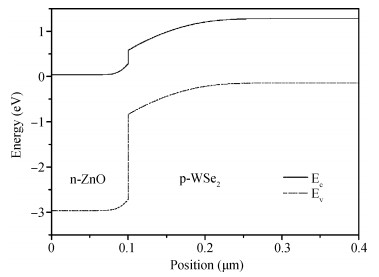
Fig. 1.
Energy band diagram for n-ZnO/p-c-WSe2 HJ structure.
SEMICONDUCTOR DEVICES
Shihua Huang, Qiannan Li, Dan Chi, Xiuqing Meng and Lü He
Corresponding author: Shihua Huang, Email: huangshihua@zjnu.cn
Abstract: Taking into account defect density in WSe2, interface recombination between ZnO and WSe2, we presented a simulation study of ZnO/crystalline WSe2 heterojunction (HJ) solar cell using wxAMPS simulation software. The optimal conversion efficiency 39.07% for n-ZnO/p-c-WSe2 HJ solar cell can be realized without considering the impact of defects. High defect density (> 1.0 × 1011 cm-2) in c-WSe2 and large trap cross-section (> 1.0 × 10⁻¹⁰ cm2) have serious impact on solar cell efficiency. A thin p-WSe2 layer is intentionally inserted between ZnO layer and c-WSe2 to investigate the effect of the interface recombination. The interface properties are very crucial to the performance of ZnO/c-WSe2HJ solar cell. The affinity of ZnO value range between 3.7-4.5 eV gives the best conversion efficiency.
Keywords: simulation, heterojunction solar cells, transport properties
| [1] |
Hossain M I, Alharbi F H. Recent advances in alternative material photovoltaics. Mater Technol, 2013, 28: 88 doi: 10.1179/1753555712Y.0000000039
|
| [2] |
Jaegermann W, Tributsch H. Interfacial properties of semiconducting transition metal chalcogenides. Progr Surf Sci, 1988, 29: 1 doi: 10.1016/0079-6816(88)90015-9
|
| [3] |
Tsirlina T, Cohen S, Cohen H, et al. Growth of crystalline WSe2 and WS2 films on amorphous substrate by reactive (Van der Waals) rheotaxy. Sol Energ Mat Sol C, 1996, 44: 457 doi: 10.1016/S0927-0248(96)00048-7
|
| [4] |
Davey B, Evans B L. The optical properties of MoTe2 and WSe2. Phys Status Solidi A, 1972, 483: 491
|
| [5] |
Bernede J C, Pouzet J, Gourmelon E, et al. Recent studies on photoconductive thin films of binary compounds. Synthetic Met, 1999, 99: 45 doi: 10.1016/S0379-6779(98)00199-4
|
| [6] |
Vogt M. Solid-state photovoltaic cells based on selenium-grown p-WSe2. PhD Thesis, University of Konstanz, 1992
|
| [7] |
Tenne R, Wold A. Passivation of recombination centers in n-WSe2 yields high efficiency ( > 14%) photo-electrochemical cell. Appl Phys Lett, 1985, 47: 707 doi: 10.1063/1.96066
|
| [8] |
Prasad G, Srivastava O N. The high-efficiency (17.1%) WSe2 photo-electrochemical solar cell. J Phys D, 1988, 21: 1028 doi: 10.1088/0022-3727/21/6/029
|
| [9] |
Joseph B, Manoj P K, Vajdyan V K. Studies on preparation and characterization of indium doped zinc oxide films by chemical spray deposition. Bull Mater Science, 2005, 28: 487 doi: 10.1007/BF02711242
|
| [10] |
Yusta F J, Hitchman M L, Shamlian S H. CVD preparation and characterization of tin dioxide films for electrochemical applications. J Mater Chem, 1997, 7: 1421 doi: 10.1039/a608525c
|
| [11] |
Vogt M, Lux-Steiner M, Dolatzoglou P, et al. Improvement of WSe2 solar cells by doping. Photovoltaic Specialists Conference, 1990
|
| [12] |
Zhu H, Kalkan A K, Hou J. Applications of AMPS-1D for solar cell simulation. Proceedings of the National Center for Photovoltaics (NCPV) 15th Program Review Meeting, 1999
|
| [13] |
Liu Y, Sun Y, Rockett A. A new simulation software of solar cells-wxAMPS. Sol Energ Mat Sol C, 2012, 98: 124 doi: 10.1016/j.solmat.2011.10.010
|
| [14] | |
| [15] |
Ma Q, Kyureghian H, Banninga J D, et al. Thin film WSe2 for use as a photovoltaic absorber material. MRS Proceedings, 2014
|
| [16] |
Gadallah A S, Nahass M M E. Structural, optical constants and photoluminescence of ZnO thin films grown by sol-gel spin coating. Adv Cond Matter Phys, 2013, 2013: 1 https://www.researchgate.net/publication/258391013_Structural_Optical_Constants_and_Photoluminescence_of_ZnO_Thin_Films_Grown_by_Sol-Gel_Spin_Coating/fulltext/55ef679508aedecb68fdad4d/258391013_Structural_Optical_Constants_and_Photoluminescence_of_ZnO_Thin_Films_Grown_by_Sol-Gel_Spin_Coating.pdf
|
| [17] |
Lang Q, Tomm Y, Schlaf R, et al. Single crystalline GaSe/WSe2 heterointerfaces grown by van der waals epitaxy. â…¡. junction characterization. J Appl Phys, 1994, 75: 7814 doi: 10.1063/1.356563
|
| [18] |
Kim M S, Yim K G, Son J S, et al. Effects of Al concentration on structural and optical properties of Al-doped ZnO thin films. Chem Soc, 2012, 33: 1235 https://www.researchgate.net/publication/276013425_Effects_of_Al_Concentration_on_Structural_and_Optical_Properties_of_Al-doped_ZnO_Thin_Films
|
| [19] |
Kim W H, Maen W J, Kim M K, et al. Low pressure chemical vapor deposition of aluminum-doped zinc oxide for transparent conducting electrodes. J Electrochem Soc, 2011, 158: D495 doi: 10.1149/1.3599055
|
| [20] |
Madelung O. Semiconductors: data handbook. 3rd ed. Springer, 2014
|
| [21] |
Huang B, Yoon M, Sumpter B G, et al. Alloy engineering of defect properties in semiconductors: suppression of deep levels in transition-metal dichalcogenides. Phys Rev Lett, 2015, 115: 126806 doi: 10.1103/PhysRevLett.115.126806
|
| [22] |
Aruchamy A. Photo-electrochemistry and photovoltaics of layered semiconductors. Kluwer Academic Publishers, Dordrecht, 1992
|
| [23] |
Klein A. Energy band alignment at interfaces of semiconducting oxides: a review of experimental determination using photoelectron spectroscopy and comparison with theoretical predictions by the electron affinity rule, charge neutrality levels, and the common anion. Thin Solid Films, 2012, 520: 3721 doi: 10.1016/j.tsf.2011.10.055
|
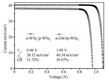
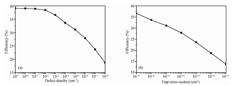
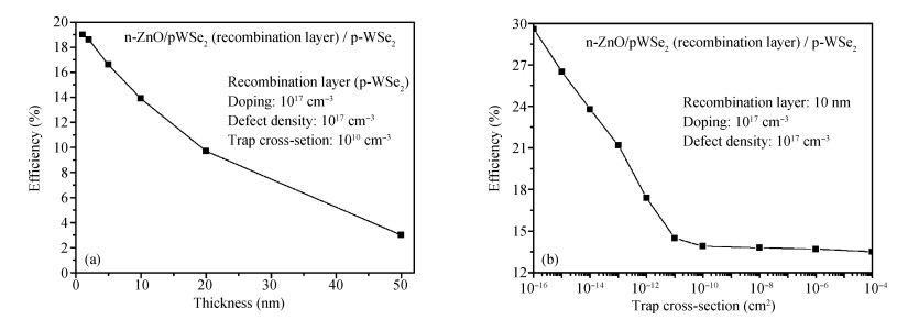
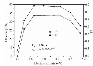
Table 1. Main parameters for simulation.

|
| [1] |
Hossain M I, Alharbi F H. Recent advances in alternative material photovoltaics. Mater Technol, 2013, 28: 88 doi: 10.1179/1753555712Y.0000000039
|
| [2] |
Jaegermann W, Tributsch H. Interfacial properties of semiconducting transition metal chalcogenides. Progr Surf Sci, 1988, 29: 1 doi: 10.1016/0079-6816(88)90015-9
|
| [3] |
Tsirlina T, Cohen S, Cohen H, et al. Growth of crystalline WSe2 and WS2 films on amorphous substrate by reactive (Van der Waals) rheotaxy. Sol Energ Mat Sol C, 1996, 44: 457 doi: 10.1016/S0927-0248(96)00048-7
|
| [4] |
Davey B, Evans B L. The optical properties of MoTe2 and WSe2. Phys Status Solidi A, 1972, 483: 491
|
| [5] |
Bernede J C, Pouzet J, Gourmelon E, et al. Recent studies on photoconductive thin films of binary compounds. Synthetic Met, 1999, 99: 45 doi: 10.1016/S0379-6779(98)00199-4
|
| [6] |
Vogt M. Solid-state photovoltaic cells based on selenium-grown p-WSe2. PhD Thesis, University of Konstanz, 1992
|
| [7] |
Tenne R, Wold A. Passivation of recombination centers in n-WSe2 yields high efficiency ( > 14%) photo-electrochemical cell. Appl Phys Lett, 1985, 47: 707 doi: 10.1063/1.96066
|
| [8] |
Prasad G, Srivastava O N. The high-efficiency (17.1%) WSe2 photo-electrochemical solar cell. J Phys D, 1988, 21: 1028 doi: 10.1088/0022-3727/21/6/029
|
| [9] |
Joseph B, Manoj P K, Vajdyan V K. Studies on preparation and characterization of indium doped zinc oxide films by chemical spray deposition. Bull Mater Science, 2005, 28: 487 doi: 10.1007/BF02711242
|
| [10] |
Yusta F J, Hitchman M L, Shamlian S H. CVD preparation and characterization of tin dioxide films for electrochemical applications. J Mater Chem, 1997, 7: 1421 doi: 10.1039/a608525c
|
| [11] |
Vogt M, Lux-Steiner M, Dolatzoglou P, et al. Improvement of WSe2 solar cells by doping. Photovoltaic Specialists Conference, 1990
|
| [12] |
Zhu H, Kalkan A K, Hou J. Applications of AMPS-1D for solar cell simulation. Proceedings of the National Center for Photovoltaics (NCPV) 15th Program Review Meeting, 1999
|
| [13] |
Liu Y, Sun Y, Rockett A. A new simulation software of solar cells-wxAMPS. Sol Energ Mat Sol C, 2012, 98: 124 doi: 10.1016/j.solmat.2011.10.010
|
| [14] | |
| [15] |
Ma Q, Kyureghian H, Banninga J D, et al. Thin film WSe2 for use as a photovoltaic absorber material. MRS Proceedings, 2014
|
| [16] |
Gadallah A S, Nahass M M E. Structural, optical constants and photoluminescence of ZnO thin films grown by sol-gel spin coating. Adv Cond Matter Phys, 2013, 2013: 1 https://www.researchgate.net/publication/258391013_Structural_Optical_Constants_and_Photoluminescence_of_ZnO_Thin_Films_Grown_by_Sol-Gel_Spin_Coating/fulltext/55ef679508aedecb68fdad4d/258391013_Structural_Optical_Constants_and_Photoluminescence_of_ZnO_Thin_Films_Grown_by_Sol-Gel_Spin_Coating.pdf
|
| [17] |
Lang Q, Tomm Y, Schlaf R, et al. Single crystalline GaSe/WSe2 heterointerfaces grown by van der waals epitaxy. â…¡. junction characterization. J Appl Phys, 1994, 75: 7814 doi: 10.1063/1.356563
|
| [18] |
Kim M S, Yim K G, Son J S, et al. Effects of Al concentration on structural and optical properties of Al-doped ZnO thin films. Chem Soc, 2012, 33: 1235 https://www.researchgate.net/publication/276013425_Effects_of_Al_Concentration_on_Structural_and_Optical_Properties_of_Al-doped_ZnO_Thin_Films
|
| [19] |
Kim W H, Maen W J, Kim M K, et al. Low pressure chemical vapor deposition of aluminum-doped zinc oxide for transparent conducting electrodes. J Electrochem Soc, 2011, 158: D495 doi: 10.1149/1.3599055
|
| [20] |
Madelung O. Semiconductors: data handbook. 3rd ed. Springer, 2014
|
| [21] |
Huang B, Yoon M, Sumpter B G, et al. Alloy engineering of defect properties in semiconductors: suppression of deep levels in transition-metal dichalcogenides. Phys Rev Lett, 2015, 115: 126806 doi: 10.1103/PhysRevLett.115.126806
|
| [22] |
Aruchamy A. Photo-electrochemistry and photovoltaics of layered semiconductors. Kluwer Academic Publishers, Dordrecht, 1992
|
| [23] |
Klein A. Energy band alignment at interfaces of semiconducting oxides: a review of experimental determination using photoelectron spectroscopy and comparison with theoretical predictions by the electron affinity rule, charge neutrality levels, and the common anion. Thin Solid Films, 2012, 520: 3721 doi: 10.1016/j.tsf.2011.10.055
|


Article views: 4764 Times PDF downloads: 39 Times Cited by: 0 Times
Received: 10 September 2016 Revised: 28 October 2016 Online: Published: 01 April 2017
| Citation: |
Shihua Huang, Qiannan Li, Dan Chi, Xiuqing Meng, Lü He. Simulation approach for optimization of ZnO/c-WSe2 heterojunction solar cells[J]. Journal of Semiconductors, 2017, 38(4): 044008. doi: 10.1088/1674-4926/38/4/044008
****
S H Huang, Q N Li, D Chi, X Q Meng, L He. Simulation approach for optimization of ZnO/c-WSe2 heterojunction solar cells[J]. J. Semicond., 2017, 38(4): 044008. doi: 10.1088/1674-4926/38/4/044008.

|
| [1] |
Hossain M I, Alharbi F H. Recent advances in alternative material photovoltaics. Mater Technol, 2013, 28: 88 doi: 10.1179/1753555712Y.0000000039
|
| [2] |
Jaegermann W, Tributsch H. Interfacial properties of semiconducting transition metal chalcogenides. Progr Surf Sci, 1988, 29: 1 doi: 10.1016/0079-6816(88)90015-9
|
| [3] |
Tsirlina T, Cohen S, Cohen H, et al. Growth of crystalline WSe2 and WS2 films on amorphous substrate by reactive (Van der Waals) rheotaxy. Sol Energ Mat Sol C, 1996, 44: 457 doi: 10.1016/S0927-0248(96)00048-7
|
| [4] |
Davey B, Evans B L. The optical properties of MoTe2 and WSe2. Phys Status Solidi A, 1972, 483: 491
|
| [5] |
Bernede J C, Pouzet J, Gourmelon E, et al. Recent studies on photoconductive thin films of binary compounds. Synthetic Met, 1999, 99: 45 doi: 10.1016/S0379-6779(98)00199-4
|
| [6] |
Vogt M. Solid-state photovoltaic cells based on selenium-grown p-WSe2. PhD Thesis, University of Konstanz, 1992
|
| [7] |
Tenne R, Wold A. Passivation of recombination centers in n-WSe2 yields high efficiency ( > 14%) photo-electrochemical cell. Appl Phys Lett, 1985, 47: 707 doi: 10.1063/1.96066
|
| [8] |
Prasad G, Srivastava O N. The high-efficiency (17.1%) WSe2 photo-electrochemical solar cell. J Phys D, 1988, 21: 1028 doi: 10.1088/0022-3727/21/6/029
|
| [9] |
Joseph B, Manoj P K, Vajdyan V K. Studies on preparation and characterization of indium doped zinc oxide films by chemical spray deposition. Bull Mater Science, 2005, 28: 487 doi: 10.1007/BF02711242
|
| [10] |
Yusta F J, Hitchman M L, Shamlian S H. CVD preparation and characterization of tin dioxide films for electrochemical applications. J Mater Chem, 1997, 7: 1421 doi: 10.1039/a608525c
|
| [11] |
Vogt M, Lux-Steiner M, Dolatzoglou P, et al. Improvement of WSe2 solar cells by doping. Photovoltaic Specialists Conference, 1990
|
| [12] |
Zhu H, Kalkan A K, Hou J. Applications of AMPS-1D for solar cell simulation. Proceedings of the National Center for Photovoltaics (NCPV) 15th Program Review Meeting, 1999
|
| [13] |
Liu Y, Sun Y, Rockett A. A new simulation software of solar cells-wxAMPS. Sol Energ Mat Sol C, 2012, 98: 124 doi: 10.1016/j.solmat.2011.10.010
|
| [14] | |
| [15] |
Ma Q, Kyureghian H, Banninga J D, et al. Thin film WSe2 for use as a photovoltaic absorber material. MRS Proceedings, 2014
|
| [16] |
Gadallah A S, Nahass M M E. Structural, optical constants and photoluminescence of ZnO thin films grown by sol-gel spin coating. Adv Cond Matter Phys, 2013, 2013: 1 https://www.researchgate.net/publication/258391013_Structural_Optical_Constants_and_Photoluminescence_of_ZnO_Thin_Films_Grown_by_Sol-Gel_Spin_Coating/fulltext/55ef679508aedecb68fdad4d/258391013_Structural_Optical_Constants_and_Photoluminescence_of_ZnO_Thin_Films_Grown_by_Sol-Gel_Spin_Coating.pdf
|
| [17] |
Lang Q, Tomm Y, Schlaf R, et al. Single crystalline GaSe/WSe2 heterointerfaces grown by van der waals epitaxy. â…¡. junction characterization. J Appl Phys, 1994, 75: 7814 doi: 10.1063/1.356563
|
| [18] |
Kim M S, Yim K G, Son J S, et al. Effects of Al concentration on structural and optical properties of Al-doped ZnO thin films. Chem Soc, 2012, 33: 1235 https://www.researchgate.net/publication/276013425_Effects_of_Al_Concentration_on_Structural_and_Optical_Properties_of_Al-doped_ZnO_Thin_Films
|
| [19] |
Kim W H, Maen W J, Kim M K, et al. Low pressure chemical vapor deposition of aluminum-doped zinc oxide for transparent conducting electrodes. J Electrochem Soc, 2011, 158: D495 doi: 10.1149/1.3599055
|
| [20] |
Madelung O. Semiconductors: data handbook. 3rd ed. Springer, 2014
|
| [21] |
Huang B, Yoon M, Sumpter B G, et al. Alloy engineering of defect properties in semiconductors: suppression of deep levels in transition-metal dichalcogenides. Phys Rev Lett, 2015, 115: 126806 doi: 10.1103/PhysRevLett.115.126806
|
| [22] |
Aruchamy A. Photo-electrochemistry and photovoltaics of layered semiconductors. Kluwer Academic Publishers, Dordrecht, 1992
|
| [23] |
Klein A. Energy band alignment at interfaces of semiconducting oxides: a review of experimental determination using photoelectron spectroscopy and comparison with theoretical predictions by the electron affinity rule, charge neutrality levels, and the common anion. Thin Solid Films, 2012, 520: 3721 doi: 10.1016/j.tsf.2011.10.055
|

 WeChat ID
Journal of Semiconductors © 2017 All Rights Reserved 京ICP备05085259号-2

 DownLoad:

