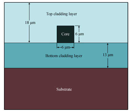
Loading [MathJax]/jax/output/HTML-CSS/jax.js
J. Semicond. > 2017, Volume 38 > Issue 4 > 044009

SEMICONDUCTOR DEVICES

Design of the low-loss waveguide coil for interferometric integrated optic gyroscopes

Yao Fei1, Tianshu Yang1, Zhaofeng Li1, Wen Liu1, Xiaodong Wang1, Wanhua Zheng2 and Fuhua Yang1,

+ Author Affiliations

 Corresponding author: Fuhua Yang, Email: fhyang@semi.ac.cn

DOI: 10.1088/1674-4926/38/4/044009

PDF

Abstract: With the development of manufacturing technology, the propagation loss of the planar waveguide is getting lower and lower, and the shot-noise-limited sensitivity of an IIOG will be greatly improved. When the propagation loss is getting lower, improper coupling-out waveguide in the waveguide coil may lead to non-ignorable bending loss and crosstalk because of the small radius of curvature and X-junction. In this paper, different coupling-out waveguides have been designed. After calculation and optimization by the beam propagation method, we found the proper coupling-out waveguide having relatively low propagation loss, which can improve the sensitivity of the IIOG.

Key words: gyroscopesSagnac effectplanar waveguidesintegrated optics

Nanostructured transition metal oxides (TMOs) are now considered as the indisputable prerequisite for developing various novel functional and smart materials. TMOs are compounds composed of oxygen atoms bound to transition metals. Copper (II) oxide (CuO) is one of the important TMOs, which plays a significant role in modern solid-state technology due to its wide range of applications such as solar cells, gas sensors, antimicrobial applications, etc.[1-4]. The benefits of using CuO in scientific and engineering applications contain its lower cost, non-toxic nature and simplicity of manufacturing. In the past few years, nanostructures of CuO with band gaps between 1.5 and 3.0 eV have been examined because of their exclusive photoluminescence and photo electro-chemical properties[1-6]. Several techniques have been employed for the fabrication of CuO thin film, such as spin-coating[7], thermal evaporation[8], pulsed laser deposition[9], chemical vapor deposition[10], molecular beam epitaxy[11], spray pyrolysis[12], etc. Among various deposition techniques, spray pyrolysis is a straightforward and cost-effective one[12]. Spray pyrolysis is a noble technique to synthesize a wide variety of good quality chemically homogeneous thin films. Large quantities of oxide thin films with homogeneous particle sizes and crystalline sizes of less than 100 nanometers may be produced by this method. The structure of CuO thin film can be influenced by doping transition metals like Zn, Mn, Co, etc.[13-15]. The ionic radius of Mn2+ is 0.83 Å, and Cu2+ is 0.73 Å[16]; because of their nearly equivalent ionic radius, it is easily possible to replace Cu2+ with Mn2+. Again, Mn2+ acts as a donor, so it can produce a free electron and enhance the electrical conductivity of CuO. Mn doping is also beneficial for tuning the optical band gap. Ferromagnetic and structural properties of radiofrequency magnetron sputtering deposited Mn-doped CuO thin films were studied by Zhao et al.[17]. They reported that the ferromagnetic behavior in Mn-doped CuO appearing from the super-exchange interactions of Mn–O–Cu–O–Mn coupling in the [10¯1] chain. Li et al.[18] performed magnetic property studies on Cu0.7Mn0.3O films prepared by the plasma-enhanced chemical vapor deposition technique and stated that the average magnetic moment was higher for the films prepared in O2 than those prepared in the air and N2 atmosphere. Mn-doped cuprous oxide thin films were prepared with x = 0–3 mM Mn concentration using electrodeposition technique, and enhancement in structure, morphology, magnetic and optical properties were reported by Ganesan et al.[19]. Durai et al.[20] prepared undoped and Mn-doped CuO (Mn:CuO) thin films via reactive radio frequency magnetron sputtering. They reported the monoclinic structure of CuO, where the average crystallite size was about 19 and 15 nm for the undoped and Mn:CuO thin films, respectively. Mishjil et al.[21] investigated optical properties of spray pyrolysis deposited Mn:CuO thin films and found that the energy gap of CuO decreased from 2 to 1.91 eV after 4% Mn doping. Manoharan et al.[22] reported a monoclinic structure of CuO nanopowder, and the band gap is reduced from 1.77 to 1.71 eV due to Mn doping. Mn-doped cuprous or cupric oxides are mostly studied to understand their magnetic properties, but extensive studies of optical and electrical properties of the material deposited by spray pyrolysis are not much reported yet. Consequently, this research aims to study the structure, surface morphology, optical and electrical transport properties of Mn:CuO thin films in detail. The prime objective of this research is to find out the suitability of Mn:CuO thin films for optoelectronic applications.

CuO and Mn:CuO thin films were deposited onto glass substrates using the spray pyrolysis technique. The glass substrates were cleaned in an ultrasonic bath using acetone, ethanol and deionized water and dried in a clean atmosphere. Copper (II) acetate monohydrate [C4H6CuO4·H2O] (purity 99%, MERCK, KGaA, 64271 Darmstadt, Germany) was used as a precursor for the deposition of CuO thin films because of its non-toxicity, non-flammable nature and water-soluble. To prepare Mn:CuO thin films, manganese acetate [Mn(CH3COO)2] (purity 99%, MERCK, KGaA, 64271 Darmstadt, Germany) was used as a doping material. At first, 0.1 M C4H6CuO4·H2O was dissolved into 100 mL distilled water and ethanol. The ratio of water and ethanol was 9 : 1. Then the mixture of materials was stirred at room temperature (300 K) for 30 min to get a homogeneous solution. To prepare the solution for deposition of Mn:CuO thin films with 2, 4, 6 and 8 atomic percentages (at%) of Mn concentrations, the ratio of the amounts of C4H6CuO4·H2O and Mn(CH3COO)2 were varied accordingly. The deposition conditions are exhibited in Table 1.

Table  1.  Parameters of CuO and Mn:CuO thin film deposition.
ParameterCondition
Spray rate during deposition1.00 mL/min
Substrate temperature350 °C
Deposition time10 min
Nozzle-to-substrate distance25 cm
Carrier air pressure0.50 bar
DownLoad: CSV  | Show Table

Film thickness was measured using the multiple beam interferometric technique (Fizeau fringe method)[23]. The thickness of 0, 2, 4, 6 and 8 at% Mn:CuO thin films were found 208, 215, 220, 232 and 238 nm, respectively. The crystal structure of CuO and Mn:CuO thin films were examined by an X-ray diffractometer [PANalytical EMPYREAN SERIES 2, Netherlands] with CuKα radiation (1.5406 Å from CuKα target operated at an input power of 60 kV). The interplanar distance was calculated using Bragg’s equation, and the peak positions were matched with the JCPDS data card no. 96-901-5925 and 96-900-5770. Field emission scanning electron microscopic (FESEM) images of the deposited samples were captured at 30 000 magnifications with a JEOL JSM-7600F (Japan) field emission scanning electron microscope. Chemical composition analysis has been carried out by an electron dispersive spectrometer (JEOL EX-37001, Japan) attached to the FESEM. Optical properties were studied at room temperature (300 K) using a UV–vis spectrophotometer (Optizen Pop, Korea). The electrical properties of the films were measured using the four-point probe method at 300 K temperature. Hall effect measurements of CuO and Mn:CuO thin films were performed at 300 K using a Hall effect measuring apparatus (ECOPIA HMS-5000, USA). The Hall effect measurements were done applying the magnetic field 0.54 T and current 3 mA.

Fig. 1 represents the FESEM images of CuO thin films with various Mn concentrations (conc.). Irregular-shaped CuO nanoparticles are seen on the surface of CuO thin films, which intends to form the different shapes of clusters. The size of CuO nanoparticles get more uniform, and the gap lessened at 2 at% Mn:CuO thin films. This may be due to the substitutions of Cu2+ ions by relatively larger sized Mn2+ ions in the CuO lattice, as a result of which molecular disorder and lattice strain are introduced and the gaps between the particles decrease[24]. Semi-spongy porous and spherical agglomerated nanocrystallites are seen on the surface of 4 at% Mn:CuO thin film. This may happen due to the origination of some secondary crystalline phases with the increased Mn2+ content. Such a semi-spongy porous microstructure may act nicely as a traping center for gas and hence be suitable for gas-sensing applications. In the FESEM image of 6 at% Mn:CuO thin film, more prominent spherical nanocrystallites are observed. It is possibly due to the relative adjustments between the primary and secondary crystalline phases upon incrementing the amount of Mn2+ between 4 to 6 at%. For 8 at% Mn doping, the surface seems to comprise non-uniformly distributed melted nanoparticle clusters, which may appear because of the excess amount of Mn2+ beyond the solid solubility limit of the dopant in the CuO lattice[13]. The formation of spherical-shaped nanoparticle clusters was found in spray pyrolysis-deposited transition metal-doped CuO thin films, such as Zn-doped CuO[13] and Cd-doped CuO[25] thin films and in spin-coated Mn:CuO thin films[26].

Figure  1.  FESEM images of Mn:CuO thin films.

Fig. 2 shows the EDX spectra of 0, 2, 4, 6 and 8 at% Mn:CuO thin films. Fig. 2(a) confirmed the presence of O and Cu elements, and Figs. 2(b)–2(e) verified the existence of Mn in the Mn:CuO thin films.

Figure  2.  (Color online) EDX spectra of (a) 0, (b) 2, (c) 4, (d) 6 and (e) 8 at% Mn:CuO thin films.

Table 2 shows the quantitative data from EDX analysis of CuO and Mn:CuO thin films. The instrumentation error corresponding to O, Cu and Mn are represented by σO, σCu and σMn in Table 1. σO, σCu and σMn values are less than 0.50, which indicates reasonable accuracy of EDX analysis.

Table  2.  Quantitative results from EDX analysis of CuO and Mn:CuO thin films.
Mn conc. in CuO (at%)at.% of element in EDX reportMn/Cu ratio
OσOCuσCuMnσMn
040.810.1858.190.480
266.360.3833.420.450.210.330.006
475.680.4423.200.431.120.420.048
660.820.3335.550.443.630.420.102
854.580.2041.260.414.170.390.101
DownLoad: CSV  | Show Table

Table 2 shows that with the increase of Mn concentration of 2, 4, 6 and 8 at% Mn:CuO thin films, the amount of Mn increases significantly in the deposited films. This is evidence of successful incorporations of Mn in CuO lattice. However, the amount of Mn in EDX analysis of Mn:CuO thin films are less than those of the expected amount of Mn in deposited films. It is revealed from the observed data that the atomic percentage (at%) of Cu decreases with the increase of Mn (conc.) in CuO. This may happen because Cu has been successfully replaced by its Mn counterpart as a dopant. The ratio of Mn to Cu (in at% units) increases with the Mn (conc.) accordingly. But for 8 at% Mn doping, it is observed that the Mn/Cu ratio is slightly decreased for 6 at% Mn doping. It may be attributed to the effect of an excess amount of Mn beyond the solid solubility limit of Mn in CuO lattice, as discussed in the surface morphology analysis.

Fig. 3 shows the XRD patterns of the as-deposited CuO and Mn:CuO thin films. X-ray diffraction (XRD) patterns show that CuO and Mn:CuO thin films were grown on the glass substrate polycrystalline nature. It is seen that all the XRD peaks match with the monoclinic CuO or tenorite phase (JCPDS card No 96-901-5 925). The crystallographic orientations of CuO thin film are detected along the (110), (¯111), (200), (ˉ202) and (¯113) planes. In the XRD pattern of 2 at% Mn:CuO, the (110) peak disappears and (¯111) and (200) peaks are slightly deviated to the higher diffraction angles due to the production of slight structural deformation associated with possible substitutions of Cu2+ ions by slightly larger Mn2+ ions in the CuO crystal lattice. By increasing Mn conc. beyond 2 at%, deviation of (110) peak to the lower and (¯111) and (200) peaks to the higher diffraction angles from the parent CuO film are observed. These may occur due to the increase of substitutions of Cu2+ ions by Mn2+ ions in the CuO lattice. Up to 2 at% Mn doping, there are no additional peaks associated with cuprous oxide (Cu2O) or Mn-impurity. When Mn conc. is increased to 4 at%, the secondary mixed phase of Cu2O (cubic phase) is observed. The Cu2O-phase persists in the XRD patterns of 6 and 8 at% Mn:CuO thin films. The secondary mixed Cu2O-phase is consistent with JCPDS card no. 96-900-5770. The possible reasons for the appearance of Cu2O-phase in the deposited thin films with 4, 6 and 8 at% Mn conc. may be the lattice asymmetry and creations of additional clustering or interstitial positions. The appearance of CuO–Cu2O mixed phases reported for Zn-doped copper oxide thin films prepared by a simple chemical deposition technique[27]. The continuous peak shift indicates that the addition of Mn2+ dopants may replace the Cu2+ site or enter into the interstitial position and may rule out the phase separation or separated nucleation of dopants.

Figure  3.  (Color online) XRD patterns of Mn:CuO thin films.

The peak positions, detected planes, crystallite sizes, average crystallite sizes, strain and dislocation densities are listed in Table 2. The Scherrer equation[28] was used to evaluate the crystallite size of CuO and Mn:CuO thin films from Fig. 3. The Scherrer equation is given as follows:

D=Kλβcosθ, (1)

where D is the crystallite size, λ = 1.5406 Å is the wavelength of Cu-Kα radiation, β is the full width at half maximum (FWHM), θ is the Bragg’s diffraction angle, and k is known as the shape factor with the value 0.89. As the Mn conc. increases, the average crystallite size increases from 17.50 to 21.30 nm. The average crystallite size values differ slightly from those reported for Mn:CuO thin films prepared by RF magnetron sputtering[20] and the sol-gel technique[22] in earlier works of literature.

Strain is another crucial structural parameter that varies depending upon the film growth conditions. It is calculated using Eq. (2)[29], where ε is the strain,

ε=βcosθ4. (2)

Strain is found to decrease as Mn conc. increases (Table 2). This reduction in strain may be due to the improvement of crystallinity at higher Mn conc. up to 6 at% and changes in surface morphology. From SEM images, it can be seen that the surface is highly compact and dense for CuO and 2, 4 and 6 at% Mn:CuO thin films. For 8 at% Mn:CuO thin film, it can be seen from SEM images that the surface comprised non-uniformly distributed melted nanoparticle clusters which cause even more reduction in strain.

Crystallite size and lattice strain were also calculated from the Williamson-Hall (W-H) plot (Fig. 4) based on the equation of uniform deformation model represented by Eq. (3)[30].

Figure  4.  (Color online) Williamson-Hall plots of Mn:CuO thin films.
βcosθ=KλD+4ϵsinθ. (3)

The W-H plots of Mn:CuO thin films with various Mn concentrations are shown in Fig. 4. The y-intercepts of the slope were used for the determination of crystallite size DW-H. Slopes of the W-H plots represent the strain values (εW-H). DW-H of 0, 2, 4, 6 and 8 at% Mn:CuO thin films are estimated to be 18, 20, 21, 26 and 28 nm, respectively. DW-H is found almost comparable with Davg in Table 2. εW-H of 0, 2, 4, 6 and 8 at% Mn:CuO thin films are computed as 5.86, 4.94, 3.88, 1.16 and 1.03 × 10⁻³, respectively. The sign of εW-H is found positive in W-H plots of Mn:CuO thin films, so the nature of strain is tensile in the films. Here, tensile strain in CuO thin film decreases with the increment of Mn doping.

The dislocation density is also an important structural parameter that determines the quality of the crystal[26]. Dislocation density can be calculated using Eq. (4)[31].

δ=1D2. (4)

Dislocation density decreases when Mn conc. increases in CuO thin films (Table 3). Because of the nearly equivalent ionic radius of Mn2+ and Cu2+, it is possible to achieve substitutional defects via Mn doping. But due to substitutional defects, Mn–O bonds appear in the films, and due to the replacements of Cu–O bonds, subsequent changes cause a reduction in dislocation density, strain, etc. The trend of variation of strain and dislocation density with Mn conc. is the opposite that of crystallite size.

Table  3.  Structural parameters of CuO and Mn:CuO thin films.
Mn conc. (at.%)2θ (deg)(hkl)D (nm)Davg (nm)ε (10–3)δ (10–3)
036.3809(¯1 11)18.8017.601.603.20
39.6309(200)16.30
236.5833(¯1 11)18.8017.50
1.613.30
39.8928(200)16.20
436.7023(¯1 11)22.6018.501.502.90
39.9642(200)14.30
636.7024(¯1 11)22.6019.501.412.60
39.8333(200)16.30
836.6429(¯1 11)28.2021.301.322.40
39.8095(200)14.30
DownLoad: CSV  | Show Table

Fig. 5 shows the absorbance spectra of the deposited CuO and Mn:CuO thin films. CuO thin film exhibits the highest absorbance in the Vis–NIR region. Absorbance decreases in 2 at% Mn:CuO thin film. Although not much significant changes are observed in the crystallinity and surface morphology of CuO thin films upon 2 at% Mn doping, the reduction in absorption suggests the successful substitution of Cu2+ by Mn2+ ions. It may be said that substitutions caused by 2 at% Mn doping maintains the growth trend of CuO crystal lattice and help to form uniform-shaped nanoparticles as found in XRD and FESEM analyses. Absorbance in the Vis-NIR region increases with Mn conc. in the range of 4 to 8 at% in CuO thin films. This increment may be ascribed to the appearance of CuO–Cu2O mixed phases in the film. The manner of variation of absorbance in Mn:CuO thin film matches nicely with that found in earlier literature[21].

Figure  5.  (Color online) Absorption spectra of Mn:CuO thin films.

The theories of optical absorption give the relation between absorption coefficient (α) and photon energy () as given below[32].

αhν=A(hνEg)n, (5)

where A is a constant, Eg is the bandgap energy of the semiconductor material, and exponent n depends on the type of transition, for allowed direct transition n = 1/2 and for allowed indirect transition n = 2[32]. The optical band gap energies related to allowed direct and indirect transitions were evaluated using the (αhν)2 versus graphs (Tauc plots) shown in Figs. 6 and 7, respectively.

Figure  6.  (Color online) Tauc plots of Mn:CuO thin films for determination of direct band gap.
Figure  7.  (Color online) Tauc plots of Mn:CuO thin films for determination of indirect band gap.

It is seen in Fig. 6 that CuO thin film has the lowest direct optical band gap of Egd ~ 2.67 eV among all the films. Egd increases between 2.71 and 2.90 eV with Mn doping up to 4 at%, and decreasing for 6 and 8 at% Mn doping. It can be explained from the XRD patterns of the films in Fig. 3. It is seen that 4, 6, and 8 at% of Mn concentrations secondary mixed-phase Cu2O (cubic phase) appears in the XRD pattern. The reason for the increase in Egd upon 4, 6 and 8 at% Mn doping may be the increase of predominance of Cu2O-cubic phase in the films. The indirect optical band gaps (Egi) of CuO and Mn:CuO thin films are estimated using Fig. 7. CuO thin film has the lowest Egi of 0.11 eV among all, whereas the highest Egi is 1.73 eV found for 2 at% Mn:CuO thin film. Egi gradually decreases with Mn concentrations from 4 to 8 at%. It can be said that the increase of dominance of the Cu2O-phase in the films causes the decreases of Egi and subsequent rise in Egd. Since the direct band gap value of the Cu2O-phase ranges between 2.20 to 2.90 eV[33, 34], which is higher compared to that of the CuO-phase, the dominance of the Cu2O-phase is observed here. Tuning of the band via mixed phases of copper oxide was reported in a published paper[33, 34]. Optical band values found for CuO and Mn:CuO are almost in agreement with those reported in earlier articles[21, 22].

The refractive index of the thin films was determined according to the Moss relation[35], which is directly associated with the fundamental energy band gap,

n=(95Eg)14eV. (6)

Another relevance between the band gap energy and the refractive index was introduced by Herve and Vandamme in the following equation[36],

n=1+(AEg+B)2, (7)

where A is the hydrogen ionization energy ~13.6 eV, and B is 3.47 eV.

Another relevance between the band gap energy and the refractive index was introduced by Ravindra, and Guptau relation is in the following equation[37],

n=4.0840.62Eg. (8)

The variation of refractive index (n) as a function of Mn concentration of the CuO thin films was also shown in Table 3 for these three models. In Table 4, it is seen that for n (Moss) and n (R-G) decreases for 0 to 4 at% Mn concentrations and then increases for 4 to 8 at% Mn concentrations and for n (H-V) follows the opposite trend. This phenomenon can be explained by the trend of variation of Egd of CuO and Mn:CuO thin films. Because Egd of CuO and Mn:CuO thin films increases with Mn doping between 0 and 4 at% and then decreases for 4 to 8 at% Mn concentrations. So, it may be remarked that the refractive index of the materials strongly depends on the band gap energy. Fig. 8 shows the variation of the refractive indices of Mn:CuO thin films with various Mn content. Refractive indices found in this work match nicely with the values reported for CuO[38, 39].

Table  4.  Optical parameters of CuO and Mn:CuO thin films.
Mn Conc. (at%)n (Moss)n (H-V)n (R-G)ε(Moss)ε(H-V)ε(R-G)ε(M-R)εomemo
02.442.752.435.967.595.907.4710.300.18
22.432.762.405.927.625.785.8410.170.17
42.392.802.295.727.825.225.699.590.04
62.412.782.355.827.715.517.169.900.12
82.432.762.395.917.645.757.4010.140.16
DownLoad: CSV  | Show Table
Figure  8.  (Color online) Variation of refractive indices of Mn:CuO thin films with various Mn content.

The equation of refractive index was derived by the Kramer–Kroning transformation (KKT). In KKT, the complex refractive index of a semiconductor can be expressed by Eq. (9)[40].

n=njk, (9)

where n and k are the real and imaginary parts of the complex refractive index. Extinction coefficient (k) was calculated using the formula,

k=αλ4π. (10)

For normal incidence, the reflectance (R) is obtained as

R=|1n+jk1+njk|2=(1n)2+k2(1+n)2+k2. (11)

The equation of refractive index (n) was derived from Eq. (11) and expressed as Eq. (12).

n=1+R1R+[4R(1R)2k2], (12)

where R is the reflectance calculated from T% and A data. Variation of n with photon wavelength is shown in Fig. 9. The maximum n-values of 0 and 2, 4, 6 and 8 at% Mn:CuO thin films are found to be 2.64, 2.66, 2.65, 2.63 and 3.58, respectively.

Figure  9.  (Color online) Variation of refractive indices of Mn:CuO thin films with photon wavelength.

In Fig. 9, n of 2 at% Mn:CuO shows its maxima at the visible region of light (wavelength 670 nm), whereas n of 0, 4, 6 and 8 at% Mn:CuO thin films show their maxima in the NIR region (wavelength 975 nm). 2 at% Mn:CuO thin film exhibits a difference in spectral variation of n, because of the reduction of the gap between particle agglomerates as seen in Fig. 1. 8 at% Mn:CuO thin film has the highest n-value among all, which is possibly due to non-uniformly distributed melted nanoparticle clusters on the film surface (Fig. 1). n (H-V)-values match nicely with n calculated from the KKT up to 6 at% Mn doping. n (H-V) of 8 at% Mn:CuO is much less compared to n calculated from the KKT. It can be said that Moss, R-G and H-V relations do not hold good when dopant concentration exceeds the solid solubility limit in the parent material. As a whole, n (H-V) is found more reasonable compared to n (Moss) and n (R-G).

The dielectric parameters of material are connected to its capacity to create obstacles in the electronic movement when it is polarized underneath the impact of an external electric field. Metal oxide semiconductors with suitable dielectric constants are required to develop efficient solar cells and other electronic devices. In this work, static and high-frequency dielectric constants were calculated for all the films. The high-frequency dielectric constant (ε) of the thin films was determined according to the Maxwell relation[40],

ϵ=n2. (13)

Adachi proposed the equation of high-frequency dielectric constant (ε) and static (εo) as follows[41],

ϵ=11.261.42Eg, (14)
ϵo=18.523.08Eg. (15)

It is seen in Table 3 that ε (Moss), ε (R-G) and ε (M-R) value decrease when Mn doping increases from 0 to 4 at%. εvalues increase in 6 and 8 at% Mn:CuO films. ε (H-V) follows the opposite trend compared to others. It is also seen that εo decreases with the increase of Mn content from 0 to 4 at% in the CuO films, and then it increases for 6 and 8 at% Mn doping. Fig. 10 shows the variation of the dielectric constant of Mn:CuO thin films with various Mn content. It may be remarked that ε and εo of the CuO and Mn:CuO strongly depends on n and Egd values.

Figure  10.  (Color online) Variation of dielectric constant of Mn:CuO thin films with various Mn content.

The electron effective mass of a semiconductor compound can be determined using the following relation[42]:

memo=5.170047.46699Eg+3.63286E2g0.57525E3g. (16)

The electron effective mass shows a decrement with the increment of Mn concentration from 0 to 4 at%, showing an increasing nature for 6 and 8 at% Mn doping in CuO thin films. The electron effective mass is noticed to be also strongly dependent on Egd, n, ε and εo. The ε, εo and memo values in this work agree with the previous works of literature[38, 43]. Observing all the dielectric parameters, it is clear that 4 at% Mn:CuO thin film has a relatively more minor tendency to create fewer obstacles to carrier movement.

Electrical properties such as resistivity (ρ), carrier concentration, mobility (μ) and Hall coefficient (RH) of the films are studied by Hall effect measurement, which is shown in Fig. 11. For the CuO thin film, the electrical resistivity is approximately 10.5 Ω·cm which is the lowest resistivity among all the films. Electrical resistivity increases with Mn doping up to 4 at% in CuO thin films, then it decreases for further increase of Mn doping. The change in electrical resistivity may occur due to a change in the stoichiometric ratio due to the more significant number of Cu ion vacancies and electrically neutral defects on the film surface[44]. Electrical resistivity of CuO thin film is found in the order of 104[13], 103[25] and 102 Ω·cm[44] for the transition metals Zn, Cd and Ni doping, respectively. The variation of the order of electrical resistivity may happen due to the difference in deposition parameters, techniques and type of dopants.

Figure  11.  (Color online) Electrical resistivity and carrier concentration Mn:CuO thin films.

The trend of variation in electrical resistivity can be understood by investigating the carrier concentration in the films. 0 and 2 at% Mn:CuO thin films have p-type carriers, and carrier concentration slightly increases upon 2 at% Mn doping. It indicates that Cu-ion vacancies are dominant for a low amount of Mn doping[44]. The type of carrier changes from p to n for 4 at% Mn doping, and carrier concentration slightly increases with the increase of Mn content in the films. For a large amount of Mn doping, there may be the predominance of surface defects over neutral vacancies. Overall, the carrier concentration is found in the order of 1017 cm–3. In earlier literature, the carrier concentration of CuO is found to vary the range of 1017 to 1019 cm–3 upon Zn, Cd, and Ni doping[13. 25, 44], respectively. Drop-in carrier concentration and change in carrier type (from p-type to n-type) are reported in earlier papers[13, 25, 44], which supports the results of Hall effect measurements.

In Fig. 12, the Hall mobility of CuO and Mn:CuO thin films vary oppositely with electrical resistivity. Hall mobility increases rapidly with Mn doping after 4 at% Mn doping CuO thin films as a result of increased n-type carriers in the film. Hall mobility of CuO and Mn:CuO thin films vary from the order of 10–1 to 100 cm2/(V·s). CuO is a material with low mobility, and Hall mobility of CuO thin films are found in the range of 10–3 – 10–1 cm2/(V·s)[44] and 10–2 cm2/(V·s)[45].

Figure  12.  (Color online) Mobility and Hall coefficient Mn:CuO thin films.

Usually, lower hole mobility arises due to higher carrier concentration, owing to the more enormous hole scattering at the native defects[46]. Since the type of carrier is changed for 4 at% Mn doping, the mobility remains constant due to the mutual charge carrier exchange processes. When the amount of Mn doping is increased beyond 4 at%, electron mobility is increased rapidly due to the increase of impurity scattering.

Hall coefficient of the films is found from 9.9–29.8 cm3/C. The Hall coefficient changed sign from positive to negative for 4 at% Mn doping and above. In Fig. 12, the absolute value of the Hall coefficient is plotted against Mn concentration in CuO thin films. Hall coefficient values indicate that 2 and 4 at% Mn:CuO films have higher carrier density with p-type carriers and less carrier density than the n-type carrier. It clearly signifies the transition in transport behavior in CuO thin film because of 4 at% Mn doping. The changes of electrical resistivity and transport behavior may be interconnected to the appearance of CuO-Cu2O mixed phases and surface morphological changes in the film, which starts appearing at 4 at% Mn doping.

Mn doping causes significant changes in the structure and properties of CuO thin films. Semi-spongy porous structures with uniformly distributed spherical nanoparticles are seen in the FESEM image of 4 at% Mn:CuO thin film, which may be very useful for gas sensing applications. In EDX analysis, Mn/Cu ratio rises with Mn doping up to 6 at% Mn doping and then it falls to 8 at% Mn doping because Mn crosses the solid solubility limits in CuO. CuO thin films show monoclinic structure up to 2 at% Mn doping. Cubic Cu2O-phase appears for 4 at% Mn doping. Cu2O-phase becomes more robust with a further increase of Mn doping. CuO film shows the maximum absorbance, and a drop of absorbance is observed for 2 and 4 at% Mn doping. The highest band gap for direct transition (2.90 eV) is estimated for 4 at% Mn:CuO thin film. The band gap for indirect transition decreased significantly with the increase of dominance of Cu2O-phase after 4 at% Mn doping. Refractive indices and dielectric constants calculated using Moss, Herve and Vandamme and Ravindra and Guptau relations suggest that Mn doping does not affect these parameters much. Refractive indices of 0 to 6 at% Mn:CuO thin films calculated using Kramer–Kroning transformation show the best match with those calculated using Herve and Vandamme relation. The most miniature electron effective mass is computed for 4 at% Mn:CuO thin films. A transition of p-type to n-type carrier is observed beyond 4 at% Mn doping which is confirmed by the sign of Hall coefficient. Electrical resistivity and Hall coefficient are the highest, whereas carrier concentration and mobility are the lowest for 4 at% Mn:CuO thin film. Structural changes and subsequent variations of properties of CuO thin films attained via Mn doping suggest the admissibility of the materials in optoelectronic applications.

The authors gratefully acknowledge the Bangladesh University of Engineering and Technology, Dhaka, Bangladesh, for financial support and the spray pyrolysis lab of the Department of Physics to perform this work. The authors are thankful to Material Science Division, Atomic Energy Center, Dhaka, Bangladesh, for providing the laboratory support for Hall effect measurements.


[1]
Li C, Zhang C, Song N, et al. Polarization-maintaining fiber loop with double optical length and its application to fiber optic gyroscope. Chin Opt Lett, 2011, 9(2): 020604 doi: 10.3788/COL
[2]
Mi J, Zhang C, Li Z, et al. Bias phase and light power dependence of the random walk coefficient of fiber optic gyroscope. Chin Opt Lett, 2006, 4(7): 379 http://en.cnki.com.cn/Article_en/CJFDTOTAL-GXKB200607003.htm
[3]
Yang Y, Zhang W, Ma J, et al. Low cost, practical, all-digital open-loop fiber-optic gyroscope. Chin Opt Lett, 2003, 1(10): 567 https://www.researchgate.net/publication/249341747_Low_cost_practical_all-digital_open-loop_fiber-optic_gyroscope
[4]
Zheng Y, Ren Y, An P, et al. Wide dynamic range experiments on a resonator fiber optic gyro based on closed-loop frequency locking technique. Chin Opt Lett, 2015, 13(2): 020601 doi: 10.3788/COL
[5]
Sagnac G. Lèher lumineux dèontrèpar l'effet du vent relatif d'èher dans un interfèomère en rotation uniforme. CR Acad Sci, 1913, 157: 708
[6]
Mottier P, Pouteau P. Solid state optical gyrometer integrated on silicon. Electron Lett, 1997, 33(23): 1975 doi: 10.1049/el:19971319
[7]
Ciminelli C, Dell'Olio F, Armenise M N. High-Q spiral resonator for optical gyroscope applications: numerical and experimental investigation. IEEE Photon J, 2012, 4(5): 1844 doi: 10.1109/JPHOT.2012.2218098
[8]
Ning L, Guo L J, Kong M, et al. Waveguide-type optical passive ring resonator gyro using frequency modulation spectroscopy technique. J Semicond, 2014, 35(12): 124008 doi: 10.1088/1674-4926/35/12/124008
[9]
Lee H, Chen T, Li J, et al. Ultra-low-loss optical delay line on a silicon chip. Nat Commun, 2012, 3: 867 doi: 10.1038/ncomms1876
[10]
Bauters J F, Heck M J, John D D, et al. Planar waveguides with less than 0. 1 dB/m propagation loss fabricated with wafer bonding. Opt Express, 2011, 19(24): 24090
[11]
Srinivasan S, Moreira R, Blumenthal D, et al. Design of integrated hybrid silicon waveguide optical gyroscope. Opt Express, 2014, 22(21): 24988 doi: 10.1364/OE.22.024988
[12]
Zhang T, Liu H, Qian Y, et al. Power loss of X-junction in solid state optical gyrometer simulated by beam propagation method. Proc SPIE, 2005, 5644: 479 doi: 10.1117/12.570300
[13]
Gundavarapu S, Huffman T, Belt M, et al. Integrated ultra-low-loss silicon nitride waveguide coil for optical gyroscopes. Opt Fiber Commun Conf, 2016
[14]
Feit M, Fleck J Jr. Light propagation in graded-index optical fibers. Appl Opt, 1978, 17(24): 3990 doi: 10.1364/AO.17.003990
[15]
Scarmozzino R, Gopinath A, Pregla R, et al. Numerical techniques for modeling guided-wave photonic devices. IEEE J Sel Top Quantum Electron, 2000, 6(1): 150 doi: 10.1109/2944.826883
[16]
Yevick D. A guide to electric field propagation techniques for guided-wave optics. Opt Quantum Electron, 1994, 26(3): S185 doi: 10.1007/BF00384672
[17]
Lefèvre H C. The fiber-optic gyroscope. Artech Hourse, 1992
[18]
Neumann E G. Curved dielectric optical waveguides with reduced transition losses. IEE Proceedings H: Microwaves Optics and Antennas, 1982
[19]
Kitoh T, Takato N, Yasu M, et al. Bending loss reduction in silica-based waveguides by using lateral offsets. J Lightw Technol, 1995, 13(4): 555 doi: 10.1109/50.372465
[20]
Ciminelli C, Dell'Olio F, Campanella C E, et al. Photonic technologies for angular velocity sensing. Adv Opt Photon, 2010, 2(3): 370 doi: 10.1364/AOP.2.000370
[21]
López-Higuera J M. Handbook of optical fibre sensing technology. Wiley, 2002
Fig. 1.  Cross section of the Archimedean spiral waveguide coil chip.

Fig. 2.  Top view of the Archimedean spiral waveguide coil. (a) Single-arc scheme for the coupling-out waveguide. (b) Double-arc scheme for the coupling-out waveguide.

Fig. 3.  Mode overlap mismatch and the optimized offset at each junction of the coupling-out waveguide "g". (a) Input side and output side mode profiles at each junction. (b) Optimized offset between the two waveguide interfaces at each junction.

Fig. 4.  Results of the bending loss calculation of the seven coupling-out waveguides of the two schemes, start radius: 8 mm. (a) Radiation losses. (b) Mode overlap losses. (c) Total bending losses. (d) Bending losses comparison between "c" and "g".

Fig. 5.  Total bending losses of coupling-out waveguide "c" and "g" under different spiral start radius.

Table 1.   Parameters of the seven coupling-out waveguides of the two schemes.

[1]
Li C, Zhang C, Song N, et al. Polarization-maintaining fiber loop with double optical length and its application to fiber optic gyroscope. Chin Opt Lett, 2011, 9(2): 020604 doi: 10.3788/COL
[2]
Mi J, Zhang C, Li Z, et al. Bias phase and light power dependence of the random walk coefficient of fiber optic gyroscope. Chin Opt Lett, 2006, 4(7): 379 http://en.cnki.com.cn/Article_en/CJFDTOTAL-GXKB200607003.htm
[3]
Yang Y, Zhang W, Ma J, et al. Low cost, practical, all-digital open-loop fiber-optic gyroscope. Chin Opt Lett, 2003, 1(10): 567 https://www.researchgate.net/publication/249341747_Low_cost_practical_all-digital_open-loop_fiber-optic_gyroscope
[4]
Zheng Y, Ren Y, An P, et al. Wide dynamic range experiments on a resonator fiber optic gyro based on closed-loop frequency locking technique. Chin Opt Lett, 2015, 13(2): 020601 doi: 10.3788/COL
[5]
Sagnac G. Lèher lumineux dèontrèpar l'effet du vent relatif d'èher dans un interfèomère en rotation uniforme. CR Acad Sci, 1913, 157: 708
[6]
Mottier P, Pouteau P. Solid state optical gyrometer integrated on silicon. Electron Lett, 1997, 33(23): 1975 doi: 10.1049/el:19971319
[7]
Ciminelli C, Dell'Olio F, Armenise M N. High-Q spiral resonator for optical gyroscope applications: numerical and experimental investigation. IEEE Photon J, 2012, 4(5): 1844 doi: 10.1109/JPHOT.2012.2218098
[8]
Ning L, Guo L J, Kong M, et al. Waveguide-type optical passive ring resonator gyro using frequency modulation spectroscopy technique. J Semicond, 2014, 35(12): 124008 doi: 10.1088/1674-4926/35/12/124008
[9]
Lee H, Chen T, Li J, et al. Ultra-low-loss optical delay line on a silicon chip. Nat Commun, 2012, 3: 867 doi: 10.1038/ncomms1876
[10]
Bauters J F, Heck M J, John D D, et al. Planar waveguides with less than 0. 1 dB/m propagation loss fabricated with wafer bonding. Opt Express, 2011, 19(24): 24090
[11]
Srinivasan S, Moreira R, Blumenthal D, et al. Design of integrated hybrid silicon waveguide optical gyroscope. Opt Express, 2014, 22(21): 24988 doi: 10.1364/OE.22.024988
[12]
Zhang T, Liu H, Qian Y, et al. Power loss of X-junction in solid state optical gyrometer simulated by beam propagation method. Proc SPIE, 2005, 5644: 479 doi: 10.1117/12.570300
[13]
Gundavarapu S, Huffman T, Belt M, et al. Integrated ultra-low-loss silicon nitride waveguide coil for optical gyroscopes. Opt Fiber Commun Conf, 2016
[14]
Feit M, Fleck J Jr. Light propagation in graded-index optical fibers. Appl Opt, 1978, 17(24): 3990 doi: 10.1364/AO.17.003990
[15]
Scarmozzino R, Gopinath A, Pregla R, et al. Numerical techniques for modeling guided-wave photonic devices. IEEE J Sel Top Quantum Electron, 2000, 6(1): 150 doi: 10.1109/2944.826883
[16]
Yevick D. A guide to electric field propagation techniques for guided-wave optics. Opt Quantum Electron, 1994, 26(3): S185 doi: 10.1007/BF00384672
[17]
Lefèvre H C. The fiber-optic gyroscope. Artech Hourse, 1992
[18]
Neumann E G. Curved dielectric optical waveguides with reduced transition losses. IEE Proceedings H: Microwaves Optics and Antennas, 1982
[19]
Kitoh T, Takato N, Yasu M, et al. Bending loss reduction in silica-based waveguides by using lateral offsets. J Lightw Technol, 1995, 13(4): 555 doi: 10.1109/50.372465
[20]
Ciminelli C, Dell'Olio F, Campanella C E, et al. Photonic technologies for angular velocity sensing. Adv Opt Photon, 2010, 2(3): 370 doi: 10.1364/AOP.2.000370
[21]
López-Higuera J M. Handbook of optical fibre sensing technology. Wiley, 2002
1

Direct or indirect band gap

Junyi Zhu

Journal of Semiconductors, 2019, 40(3): 030202. doi: 10.1088/1674-4926/40/3/030202

2

Influence of precursor solution concentration on the structural, optical and humidity sensing properties of spray-deposited TiO2 thin films

Dipak L Gapale, Sandeep A Arote, Balasaheb M Palve, Ratan Y Borse

Journal of Semiconductors, 2018, 39(12): 122003. doi: 10.1088/1674-4926/39/12/122003

3

Effect of substrate temperature on the physical properties of SnS2:Cu thin films deposited by spray pyrolysis

M. R. Fadavieslam

Journal of Semiconductors, 2018, 39(12): 123005. doi: 10.1088/1674-4926/39/12/123005

4

Synthesis and characterization of ZnO–CuO nanocomposites powder by modified perfume spray pyrolysis method and its antimicrobial investigation

D. Saravanakkumar, S. Sivaranjani, K. Kaviyarasu, A. Ayeshamariam, B. Ravikumar, et al.

Journal of Semiconductors, 2018, 39(3): 033001. doi: 10.1088/1674-4926/39/3/033001

5

Influence of band gap of p-type hydrogenated nanocrystalline silicon layer on the short-circuit current density in thin-film silicon solar cells

Shuwei Zhang, Xiangbo Zeng

Journal of Semiconductors, 2017, 38(11): 114007. doi: 10.1088/1674-4926/38/11/114007

6

Substrate temperature dependent studies on properties of chemical spray pyrolysis deposited CdS thin films for solar cell applications

Kiran Diwate, Amit Pawbake, Sachin Rondiya, Rupali Kulkarni, Ravi Waykar, et al.

Journal of Semiconductors, 2017, 38(2): 023001. doi: 10.1088/1674-4926/38/2/023001

7

Electrical properties of Cu4ZnSnS2/ZnS heterojunction prepared by ultrasonic spray pyrolysis

S. Guitouni, M. Khammar, M. Messaoudi, N. Attaf, M.S. Aida, et al.

Journal of Semiconductors, 2016, 37(12): 122001. doi: 10.1088/1674-4926/37/12/122001

8

Structural and opto-electrical properties of pyrolized ZnO-CdO crystalline thin films

A. M. M. Tanveer Karim, M. K. R. Khan, M. Mozibur Rahman

Journal of Semiconductors, 2015, 36(5): 053001. doi: 10.1088/1674-4926/36/5/053001

9

Structural, optical and electrical properties of zinc oxide thin films deposited by a spray pyrolysis technique

Yacine Aoun, Boubaker Benhaoua, Brahim Gasmi, Said Benramache

Journal of Semiconductors, 2015, 36(1): 013002. doi: 10.1088/1674-4926/36/1/013002

10

The calculation of band gap energy in zinc oxide films

Ali Arif, Okba Belahssen, Salim Gareh, Said Benramache

Journal of Semiconductors, 2015, 36(1): 013001. doi: 10.1088/1674-4926/36/1/013001

11

Effect of band gap energy on the electrical conductivity in doped ZnO thin film

Said Benramache, Okba Belahssen, Hachemi Ben Temam

Journal of Semiconductors, 2014, 35(7): 073001. doi: 10.1088/1674-4926/35/7/073001

12

Synthesis of In2S3 thin films by spray pyrolysis from precursors with different[S]/[In] ratios

Thierno Sall, A. Nafidi, Bernabé Marí Soucase, Miguel Mollar, Bouchaib Hartitti, et al.

Journal of Semiconductors, 2014, 35(6): 063002. doi: 10.1088/1674-4926/35/6/063002

13

Ultrasonic spray pyrolysis deposition of SnSe and SnSe2 using a single spray solution

Jorge Sergio Narro-Rios, Manoj Ramachandran, Dalia Martínez-Escobar, Aarón Sánchez-Juárez

Journal of Semiconductors, 2013, 34(1): 013001. doi: 10.1088/1674-4926/34/1/013001

14

Effect of Fe-doping on the structural and optical properties of ZnO thin films prepared by spray pyrolysis

S.M. Salaken, E. Farzana, J. Podder

Journal of Semiconductors, 2013, 34(7): 073003. doi: 10.1088/1674-4926/34/7/073003

15

Spray pyrolysis of tin selenide thin-film semiconductors:the effect of selenium concentration on the properties of the thin films

M. R. Fadavieslam, M. M. Bagheri-Mohagheghi

Journal of Semiconductors, 2013, 34(8): 082001. doi: 10.1088/1674-4926/34/8/082001

16

Correlation between electrical conductivity-optical band gap energy and precursor molarities ultrasonic spray deposition of ZnO thin films

Said Benramache, Okba Belahssen, Abderrazak Guettaf, Ali Arif

Journal of Semiconductors, 2013, 34(11): 113001. doi: 10.1088/1674-4926/34/11/113001

17

Effect of deposition conditions on the physical properties of SnxSy thin films prepared by the spray pyrolysis technique

M. R. Fadavieslam, N. Shahtahmasebi, M. Rezaee-Roknabadi, M. M. Bagheri-Mohagheghi

Journal of Semiconductors, 2011, 32(11): 113002. doi: 10.1088/1674-4926/32/11/113002

18

Growth of High AI Content AIGaN Epilayer by MOCVD

Wang Xiaoyan, Wang Xiaoliang, Hu Guoxin, Wang Baozhu, Li Jianping, et al.

Chinese Journal of Semiconductors , 2007, 28(S1): 193-196.

19

Effects of Growth Temperature Oil the InAIGaN Epilayer by RF-MBE

Wang Baozhu, Wang Xiaoliang, Wang Xiaoyan, Wang Xinhua, Guo Lunchun, et al.

Chinese Journal of Semiconductors , 2007, 28(S1): 197-199.

20

Effect of Different Facets of on the Growth of vapor deposition

Zhang Panfeng, Wei Hongyuan, Fan Haibo, Cong Guangwei, Yang Shaoyan, et al.

Chinese Journal of Semiconductors , 2007, 28(S1): 289-292.

1. Lucky, S.A., Sharmin, M., Das, H. et al. Evolution in morphological features, enhancement of optical transparency and band gap broadening in Manganese doped nickel oxide thin films for optoelectronics applications. Thin Solid Films, 2025. doi:10.1016/j.tsf.2025.140651
2. Rahaman, R., Sharmin, M., Podder, J. The effect of cobalt doping on the structure and properties of copper oxide thin films: Evolution in surface morphology, p- to n-type carrier transition and enhancement optoelectronic behavior. International Journal of Modern Physics B, 2025. doi:10.1142/S0217979225501450
3. Hussein, B., Imer, A.G., Aycibin, M. Influence of substrate temperature and Mn/Y co-doping concentration on the morphological, structural and optical properties of CuO nanostructured film deposited by the spray pyrolysis method. Physica B: Condensed Matter, 2025. doi:10.1016/j.physb.2024.416674
4. Nam, D.T., Trinh, B.N.Q. Structural, optical, and electrical properties of multi-component P-type oxide-semiconductor Cu-Mn-Sn-O thin films. Thin Solid Films, 2024. doi:10.1016/j.tsf.2024.140441
5. Talapatra, S., Das, U., Galib, M. et al. Enhanced opto-electronic properties of Nd doped CuO thin film. Ceramics International, 2024, 50(16): 27699-27709. doi:10.1016/j.ceramint.2024.05.067
6. Kumar, P.S., Johnson, J., Biju, C.S. Structural, morphological, and optoelectronic characteristics of Zn, Cd-co-doped CuO nanostructures. Journal of Materials Science: Materials in Electronics, 2024, 35(18): 1233. doi:10.1007/s10854-024-13010-8
7. Hortêncio, J.D.S., Lourenço, A.D.A., Raimundo, R.A. et al. MOF-templated CuO and Mn[sbnd]CuO/Cu2O composites as electrocatalyst in oxygen evolution. Journal of Molecular Structure, 2024. doi:10.1016/j.molstruc.2023.137018
8. Alotibi, T., Shirbeeny, W., Alshahrie, A. et al. Time-Resolved Sensitivity of a Cadmium-Doped Copper Oxide Thin Film as a Chlorine Gas Detector. Advances in Science and Technology Research Journal, 2024, 18(2): 365-373. doi:10.12913/22998624/185270
9. Alshammari, R.H., Aadil, M., Kousar, T. et al. Synthesis of Binary Metal Doped CuO Nanoarchitecture for Congo red dye Removal: Synergistic Effects of Adsorption and Mineralization Techniques. Optical Materials, 2023. doi:10.1016/j.optmat.2023.114314
10. Banu, T., Jamal, M., Gulshan, F. Opto-structural properties and photocatalytic activities of CuO NPs synthesized by modified sol-gel and Co-precipitation methods: A comparative study. Results in Materials, 2023. doi:10.1016/j.rinma.2023.100419
11. Soltanian, A., Ghasemi, M., Eftekhari, L. et al. Correlation between the optical and microstructural characteristics and surface wettability transition of In2O3:Sn/ZnO nanostructured bilayer system for self-cleaning application. Physica Scripta, 2023, 98(7): 075912. doi:10.1088/1402-4896/acd9fd
12. Jabr, M.A., Ali, A.M., Ismail, R.A. Preparation of high-performance p-CuO/n-Si heterojunction photodetector by laser-assisted chemical bath deposition: Effect of laser wavelength. Ceramics International, 2023, 49(7): 11442-11451. doi:10.1016/j.ceramint.2022.11.343
13. Jamal, M., Billah, M.M., Ayon, S.A. Opto-structural and magnetic properties of fluorine doped CuO nanoparticles: An experimental study. Ceramics International, 2023, 49(6): 10107-10118. doi:10.1016/j.ceramint.2022.11.194
14. Wisz, G., Sawicka-Chudy, P., Wal, A. et al. Structure Defects and Photovoltaic Properties of TiO2:ZnO/CuO Solar Cells Prepared by Reactive DC Magnetron Sputtering. Applied Sciences (Switzerland), 2023, 13(6): 3613. doi:10.3390/app13063613
15. Mallick, P.. Band-gap engineering of ceramic coatings. Advanced Ceramic Coatings: Fundamentals, Manufacturing, and Classification, 2023. doi:10.1016/B978-0-323-99659-4.00007-3
16. Zhong, L., Li, X., Wang, W. et al. Electromechanical and photoelectric properties of a novel semiconducting Janus InGaSSe monolayer. Journal of Semiconductors, 2023, 44(1): 012701. doi:10.1088/1674-4926/44/1/012701
17. Al Armouzi, N., Manoua, M., Hilal, H.S. et al. Multi-Layered Sol–Gel Spin‐Coated CuO Nanofilm Characteristic Enhancement by Sn Doping Concentration. Processes, 2022, 10(7): 1277. doi:10.3390/pr10071277
18. Güneri, E., Johnson, H., Göde, F. Chemical Bath Deposition Grown ZnO Thin Films: Role of Manganese Doping. Journal of Nano Research, 2022. doi:10.4028/p-0feb08
  • Search

    Advanced Search >>

    GET CITATION

    R. Rahaman, M. Sharmin, J. Podder. Band gap tuning and p to n-type transition in Mn-doped CuO nanostructured thin films[J]. Journal of Semiconductors, 2022, 43(1): 012801. doi: 10.1088/1674-4926/43/1/012801
    R Rahaman, M Sharmin, J Podder, Band gap tuning and p to n-type transition in Mn-doped CuO nanostructured thin films[J]. J. Semicond., 2022, 43(1): 012801. doi: 10.1088/1674-4926/43/1/012801.
    shu

    Export: BibTex EndNote

    Article Metrics

    Article views: 3357 Times PDF downloads: 20 Times Cited by: 18 Times

    History

    Received: 22 April 2016 Revised: 18 October 2016 Online: Published: 01 April 2017

    Catalog

      Email This Article

      User name:
      Email:*请输入正确邮箱
      Code:*验证码错误
      R. Rahaman, M. Sharmin, J. Podder. Band gap tuning and p to n-type transition in Mn-doped CuO nanostructured thin films[J]. Journal of Semiconductors, 2022, 43(1): 012801. doi: 10.1088/1674-4926/43/1/012801 ****R Rahaman, M Sharmin, J Podder, Band gap tuning and p to n-type transition in Mn-doped CuO nanostructured thin films[J]. J. Semicond., 2022, 43(1): 012801. doi: 10.1088/1674-4926/43/1/012801.
      Citation:
      Yao Fei, Tianshu Yang, Zhaofeng Li, Wen Liu, Xiaodong Wang, Wanhua Zheng, Fuhua Yang. Design of the low-loss waveguide coil for interferometric integrated optic gyroscopes[J]. Journal of Semiconductors, 2017, 38(4): 044009. doi: 10.1088/1674-4926/38/4/044009 ****
      Y Fei, T S Yang, Z F Li, W Liu, X D Wang, W H Zheng, F H Yang. Design of the low-loss waveguide coil for interferometric integrated optic gyroscopes[J]. J. Semicond., 2017, 38(4): 044009. doi: 10.1088/1674-4926/38/4/044009.

      Design of the low-loss waveguide coil for interferometric integrated optic gyroscopes

      DOI: 10.1088/1674-4926/38/4/044009
      Funds:

      the National Natural Science Foundation of China 61274066

      the National Natural Science Foundation of China 61504138

      the National Natural Science Foundation of China 61504138

      the National Key Research and Development Program of China 2016YFA02005003

      Project supported by the National Natural Science Foundation of China (Nos. 61274066, 61504138, c) and the National Key Research and Development Program of China (No. 2016YFA02005003)

      More Information
      • Corresponding author: Fuhua Yang, Email: fhyang@semi.ac.cn
      • Received Date: 2016-04-22
      • Revised Date: 2016-10-18
      • Published Date: 2017-04-01

      Catalog

        /

        DownLoad:  Full-Size Img  PowerPoint
        Return
        Return