| Citation: |
B. Shougaijam, R. Swain, C. Ngangbam, T.R. Lenka. Analysis of morphological, structural and electrical properties of annealed TiO2 nanowires deposited by GLAD technique[J]. Journal of Semiconductors, 2017, 38(5): 053001. doi: 10.1088/1674-4926/38/5/053001
****
B Shougaijam, R Swain, C Ngangbam, T R Lenka. Analysis of morphological, structural and electrical properties of annealed TiO2 nanowires deposited by GLAD technique[J]. J. Semicond., 2017, 38(5): 053001. doi: 10.1088/1674-4926/38/5/053001.
|
Analysis of morphological, structural and electrical properties of annealed TiO2 nanowires deposited by GLAD technique
DOI: 10.1088/1674-4926/38/5/053001
More Information
-
Abstract
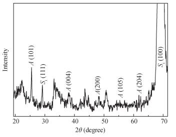
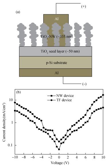
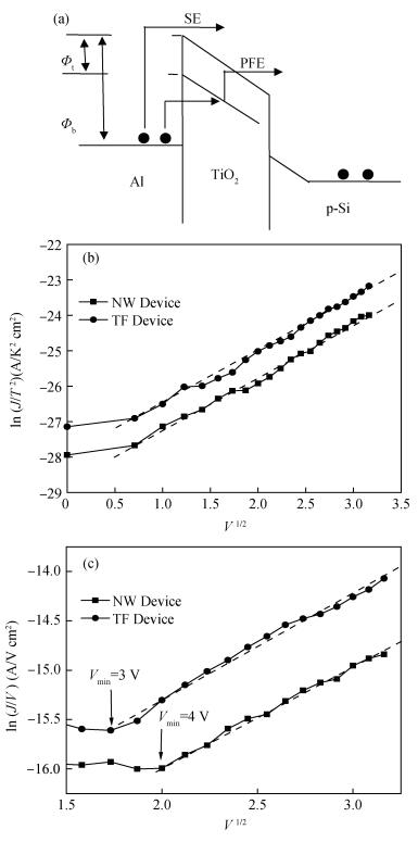
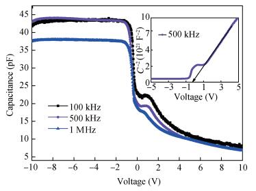
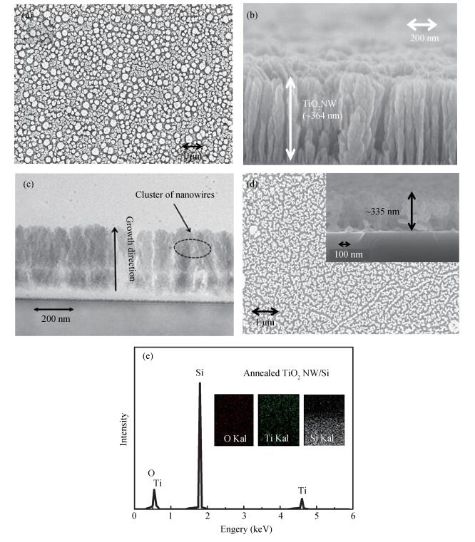
The effect of annealing on vertically aligned TiO2 NWs deposited by glancing angle deposition (GLAD) method on Si substrate using pressed and sintered TiO2 pellets as source material is studied.The FE-SEM images reveal the retention of vertically aligned NWs on Si substrate after annealing process.The EDS analysis of TiO2 NWs sample annealed at 600 ℃ in air for 1 h shows the higher weight percentage ratio of ~2.6(i.e., 72.27% oxygen and 27.73% titanium).The XRD pattern reveals that the polycrystalline nature of anatase TiO2 dominates the annealed NWs sample.The electrical characteristics of Al/TiO2-NWs/TiO2-TF/p-Si (NW device) and Al/TiO2-TF/p-Si (TF device) based on annealed samples are compared.It is riveting to observe a lower leakage current of ~1.32×10⁻⁷ A/cm2 at+1 V with interface trap density of ~6.71×10¹¹ eV-1cm-2 in NW device compared to ~2.23×10⁻⁷ A/cm2 in TF device.The dominant leakage mechanism is investigated to be generally Schottky emission; however Poole-Frenkel emission also takes place during high reverse bias beyond 4 V for NWs and 3 V for TF device.-
Keywords:
- annealing,
- GLAD,
- morphology,
- nanowires,
- structural,
- TiO2
-
References
[1] San S R. Analysis of optoelectronic properties of TIO2 nanowires/Si heterojunction arrays. Chin Phys B, 2014, 23: 107302 doi: 10.1088/1674-1056/23/10/107302[2] Li H L, Yu Q J, Huang Y W. Ultralong rutile TIO2 nanowire arrays for highly efficient dye-sensitized solar cells. Appl Mater Interfaces, 2016, 8: 13384 doi: 10.1021/acsami.6b01508[3] Tian W, Ho Y, Chen C, et al. Sensing performance of precisely ordered TIO2 nanowire gas sensors fabricated by electron-beam lithography. Sensors, 2013, 13: 865 doi: 10.3390/s130100865[4] Xie Y, Wei L, Wei G, et al. A self-powered UV photodetector based on TIO2 nanorod arrays. Nanoscale Res Lett, 2013, 8: 188 doi: 10.1186/1556-276X-8-188[5] Yu Y, Yin X, Kvit A, et al. Evolution of hollow TIO2 nanostructures via the Kirkendall effect driven by cation exchange with enhanced photoelectrochemical performance. Nano Lett, 2014, 14: 2528 doi: 10.1021/nl5002907[6] Zhang W, Cunningham B T. Biosensors with porous dielectric surface for fluorescence enhancement and methods of manufacture. US Patent, 7869032B2, 2011[7] Wilka G D, Wallace R M, Anthony J M. High-k gate dielectrics: current status and materials properties considerations. J Appl Phys, 2001, 89: 5243 doi: 10.1063/1.1361065[8] Luisier M, Schenk A. Two-dimensional tunneling effects on the leakage current of MOSFETs with single dielectric and high-k gate stacks. IEEE Trans Electron Dev, 2008, 55: 6 http://ieeexplore.ieee.org/document/4495122/[9] Rajwali K, Zulfiqar, Simbarashe F. Magnetic and dielectric properties of (Co, Zn) co-doped SnO2 diluted magnetic semiconducting nanoparticles. J Mater Sci: Mater Electron, 2016, 27: 5960 doi: 10.1007/s10854-016-4517-2[10] Kumar A, Mondal S, Kumar S G, et al. High performance solgel spin-coated titanium dioxide dielectric based MOS structures. Mat Sci Semicond Proc, 2015, 40: 77 doi: 10.1016/j.mssp.2015.06.073[11] Negara M A, Kitano M, Long R D. Oxide charge engineering of atomic layer deposited AlOxNy/Al2O3 gate dielectrics: a path to enhancement mode GaN devices. Appl Mater Interfaces, 2016, 8: 21089 doi: 10.1021/acsami.6b03862[12] Mahajan A M, Anil G K, Thibeault B J. High dielectric constant ZrO2 films by atomic layer deposition technique on germanium substrates. Silicon, 2016, 8: 345 doi: 10.1007/s12633-015-9322-7[13] Jiro Y, Hong S, Ravi R. Characterization of atomic layer deposition HfO2, Al2O3, and plasma-enhanced chemical vapor deposition Si3N4 as metal-insulator-metal capacitor dielectric for GaAs HBT technology. J Vac Sci Technol, 2013, 31: 01A134 http://ieeexplore.ieee.org/document/6375995/[14] Dervos C T, Thirios E, Novacovich J, et al. Permittivity properties of thermally treated TIO2. Mater Lett, 2004, 58: 1502 doi: 10.1016/j.matlet.2003.10.012[15] Yang Y, Qu L, Dai L, et al. Coating of titanium dioxide on aligned carbon nanotubes for controlled syntheses of photoelectronic nanomaterials. Adv Mater, 2007, 19: 1239 doi: 10.1002/(ISSN)1521-4095[16] Sönmezoglu S, Akin S. Current transport mechanism of antimony-doped TIO2 nanoparticles based on MOS device. Sensors Actuat A, 2013, 199: 18 doi: 10.1016/j.sna.2013.04.037[17] Yang W, Marino J, Monson A, et al. An investigation of annealing on the dielectric performance of TIO2 thin films. Semicond Sci Technol, 2006, 21: 1573 doi: 10.1088/0268-1242/21/12/012[18] Vishwas M, Narasimha R K, Chakradhar R P S, et al. Effect of film thickness and annealing on optical properties of TIO2 thin films and electrical characterization of MOS capacitors. J Mater Sci: Mater Electron, 2014, 25:4495 doi: 10.1007/s10854-014-2193-7[19] Frank M M, Kim S, Brown S L, Bruley J, et al. Scaling the MOSFET gate dielectric: from high-k to higher-k. Microelectron Eng, 2009, 86: 1603 doi: 10.1016/j.mee.2009.03.063[20] Perego M, Seguini G, Scarel G, et al. Energy band alignment at TIO2/Si interface with various interlayers. J Appl Phys, 2008, 103: 043509 doi: 10.1063/1.2885109[21] Bae G, Song Y, Jung D, et al. Significant reduction of leakage current in the TIO2/Si structure by the insertion of the CeO2 intermediate layer. Appl Phys Lett, 2000, 77: 729 doi: 10.1063/1.127100[22] Chinnamuthu P, Mondal A, Singh N K, et al. Band gap enhancement of glancing angle deposited TIO2 nanowire array. J Appl Phys, 2012, 112: 054315 doi: 10.1063/1.4749801[23] Aniruddha M, Jay C D, Chinnamuthu P, et al. Electrical properties of vertically oriented TIO2 nanowire arrays synthesized by glancing angle deposition technique. Electron Mater Lett, 2013, 9: 213 doi: 10.1007/s13391-012-2136-5[24] Li Z C, Zhu Y, Zhou Q, et al. Photocatalytic properties of TIO2 thin films obtained by glancing angle deposition. Appl Surf Sci, 2012, 258: 2766 doi: 10.1016/j.apsusc.2011.10.129[25] Viktor L, Matthew H, Andriy K, et al. Omnidirectional reflection from nanocolumnar TIO2 films. J Appl Phys, 2012, 112: 084317 doi: 10.1063/1.4759138[26] Biraj S, Swain R, Ngangbam C, et al. Enhanced photodetection by glancing angle deposited vertically aligned TIO2 nanowires. IEEE Trans Nanotechnol, 2016, 15: 389 doi: 10.1109/TNANO.2016.2536162[27] Zhou C M, Gall D. Growth competition during glancing angle deposition of nanorod honeycomb arrays. Appl Phys Lett, 2007, 90: 093103 doi: 10.1063/1.2709929[28] Jang H K, Whangbo S W, Kim H B. Titanium oxide films on Si (100) deposited by electron-beam evaporation at 250℃. J Vac Sci Technol A, 2000, 18: 917 doi: 10.1116/1.582275[29] Wang B, Qi H J, Wang H, et al. Morphology, structure and optical properties in TIO2 nanostructured films annealed at various temperatures. Opt Mater Express, 2015, 5: 1410 doi: 10.1364/OME.5.001410[30] Khan A F, Mehmood M, Durrani S K, et al. Structural and optoelectronic properties of nanostructured TIO2 thin films with annealing. Mat Sci Semicond Proc, 2015, 29: 161 doi: 10.1016/j.mssp.2014.02.009[31] Chakraborty S, Bera M K, Bhattacharya S, et al. Current conduction mechanism in TIO2 gate dielectrics. Microelectron Eng, 2005, 81: 188 doi: 10.1016/j.mee.2005.03.005[32] Lee M K, Huang J J, Wu T S. Electrical characteristics improvement of oxygen-annealed MOCVD-TIO2 films. Semicond SciTechnol, 2005, 20: 519 https://www.researchgate.net/publication/230921146_Electrical_characteristics_improvement_of_oxygen-annealed_MOCVD-TiO2_films[33] Liu Z H, Ng G I, Arulkumaran S, et al. Temperaturedependent forward gate current transport in atomic-layer deposited Al2O3/AlGaN/GaN metal-insulator-semiconductor high electron mobility transistor. Appl Phys Lett, 2011, 98: 63501 doi: 10.1063/1.3554364[34] Perera R, Ikeda A, Hattori R, et al. Trap assisted leakage current conduction in thin silicon oxynitride films grown by rapid thermal oxidation combined microwave excited plasma nitridation. Microelectron Eng, 2003, 65: 357 doi: 10.1016/S0167-9317(02)01025-0[35] Kwa K S K, Chattopadhyay S, Jankovic N D, et al. A model for capacitance reconstruction from measured lossy MOS capacitance-voltage characteristics. Semicond Sci Technol, 2003, 18: 82 doi: 10.1088/0268-1242/18/2/303[36] Hill W A, Coleman C C. A single-frequency approximation for interface-state density determination. Solid State Electron, 1989, 23: 987 http://www.sciencedirect.com/science/article/pii/0038110180900647[37] Pakma O, Serin N, Serin T, et al. On the energy distribution profile of interface states obtained by taking into account of series resistance in Al/TIO2/p-Si (MIS) structures. Physica B, 2011, 406: 771 doi: 10.1016/j.physb.2010.11.078 -
Proportional views


 DownLoad:
