


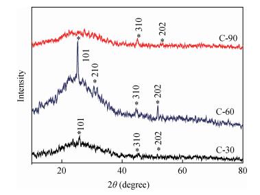
Fig. 1.
XRD pattern of Cu$_{3}$ Se$_{2}$ films deposited at various growth time by chemical bath deposition at room temperature.
SEMICONDUCTOR MATERIALS
Balasaheb M. Palve1, 2, Sandesh R. Jadkar1 and Habib M. Pathan1,
Corresponding author: Habib M. Pathan Email:arjunpalve@gmail.com
Abstract: Copper selenide (Cu3Se2)thin films have been synthesized with Se as the precursor in aqueous solution by chemical bath deposition technique at room temperature. We have investigated the influence of the growth time ranging from 30 to 90 min on structural, optical and electrical properties of Cu3Se2 thin films. The as-grown film at 60 min exhibits a tetragonal structure and is (101) oriented. The maximum value of crystal size D= 55 nm is attained for Cu3Se2 films grown at 60 min. The Raman spectrum reveals a pronounced peak at 259 cm-1, which is assigned to vibrational (stretching) modes from the covalent Se-Se bonds. The optical band gap energy is 1.91 to 2.01 eV with growth time increased from 30 to 90 min. The scanning electron microscopy (SEM) study reveals that the grains are uniform and spread over the entire surface of the substrate of the film at 60 min. The Hall effect study reveals that the film exhibits p-type conductivity. The synthesized film showed good absorbance in the visible region which signifies that synthesized Cu3Se2 films can be suitable as a sensitized material in semiconductor sensitized solar cells.
Keywords: copper selenide, thin film, growth time, Raman spectrum
| [1] |
Yin Y, Alivisatos A P. Colloidal nanocrystal synthesis and the organic-inorganic interface. Nature, 2005, 437:664 doi: 10.1038/nature04165
|
| [2] |
Peng Z A, Peng X G. Formation of high-quality CdTe, CdSe, and CdS nanocrystals using CdO as precursor. J Am Chem Soc, 2001, 123:183 doi: 10.1021/ja003633m
|
| [3] |
Yoon H, Granata J, Hebert P, et al. Recent advances in highefficiency Ⅲ-Ⅴ multi-junction solar cells for space applications:ultra triple junction qualification. Prog Photovolt Res Appl, 2005, 13:133 doi: 10.1002/(ISSN)1099-159X
|
| [4] |
Auffan M, Rose J, Bottero J Y, et al. Towards a definition of inorganic nanoparticles from an environmental, health and safety perspective nature. Nanotechnology, 2009, 4:634 http://hero.epa.gov/index.cfm?action=search.view&reference_id=199803
|
| [5] |
Brown G F, Wu J. Third generation photovoltaics. Laser Photon, 2009, 3:394 doi: 10.1002/(ISSN)1863-8899
|
| [6] |
Trindade T, O'Brien P, Pickett N L, et al. Nanocrystalline semiconductors:synthesis, properties, and perspectives. Chem Mater. 2001, 13:3843 doi: 10.1021/cm000843p
|
| [7] |
Schaller R D, Klimov V I. High efficiency carrier multiplication in PbSe nanocrystals:implications for solar energy conversion. Phys Rev Lett, 2004, 92:186601 doi: 10.1103/PhysRevLett.92.186601
|
| [8] |
Gracia V M, Nair P K, Nair M T S, et al. Copper selenide thin films by chemical bath deposition. J Cryst Growth, 1999, 203:113 doi: 10.1016/S0022-0248(99)00040-8
|
| [9] |
Riha S C, Johnson D C, Prieto A L, et al. Cu2Se nanoparticles with tunable electronic properties due to a controlled solid-state phase transition driven by copper oxidation and cationic conduction. J Am Chem Soc, 2010, 133:383 https://www.ncbi.nlm.nih.gov/pubmed/21033686/
|
| [10] |
Estrada C A, Nair P K, Nair M T S, et al. Chemical bath deposition of ZnSe and CuSe thin films using N, N-dimethylselenourea. J Electrochem Soc, 1994, 141:802 doi: 10.1149/1.2054814
|
| [11] |
Schafer A, Kouwitz M, Ahlrichs R, et al. Electronic excitation energies in copper selenide clusters. J Chem Phys, 1996, 104:7113 doi: 10.1063/1.471404
|
| [12] |
Hermann A M, Fabick L. Research on polycrystalline thin-film photovoltaic devices. J Cryst Growth, 1983, 61:658 doi: 10.1016/0022-0248(83)90195-1
|
| [13] |
Peranantham P, Jeyachandran Y L, Viswanathan C, et al. The effect of annealing on vacuum-evaporated copper selenide and indium telluride thin films. Mater Charact, 2007, 58:756 doi: 10.1016/j.matchar.2006.11.019
|
| [14] |
Moysiadou A, Koutsikou R, Bouroushian R, et al. Pulse electrodeposition of copper selenide from acidic aqueous baths. Mater Lett, 2015, 139:112 doi: 10.1016/j.matlet.2014.10.036
|
| [15] |
Levy-Clement C, Neumann-Spallart M, Haram S K, et al. Chemical bath deposition of cubic copper (Ⅰ) selenide and its room temperature transformation to the orthorhombic phase. Thin Solid Films, 1997, 302:12 doi: 10.1016/S0040-6090(97)00021-7
|
| [16] |
Lakshmi M, Bindu K, Bini S, et al. Reversible Cu2-xSe↔Cu3Se2 phase transformation in copper selenide thin films prepared by chemical bath deposition. Thin Solid Films, 2001, 386:127 doi: 10.1016/S0040-6090(00)01783-1
|
| [17] |
Mane R S, Kajve S P, Lokhande C D, et al. Studies on p-type copper (Ⅰ) selenide crystalline thin films for hetero-junction solar cells. Vacuum, 2006, 80:631 doi: 10.1016/j.vacuum.2005.08.021
|
| [18] |
Pathan H M, Lokhande C D, Amalnerkar D P, et al. Modified chemical deposition and physico-chemical properties of copper (Ⅰ) selenide thin films. Appl Surf Sci, 2003, 211:48 doi: 10.1016/S0169-4332(03)00046-1
|
| [19] |
Bi H, Zhao W, Sun S, et al. Graphene films decorated with metal sulfide nanoparticles for use as counter electrodes of dyesensitized solar cells. Carbon, 2013, 61:116 doi: 10.1016/j.carbon.2013.04.075
|
| [20] |
Balis N, Dracopoulos V, Bourikas K, et al. Quantum dot sensitized solar cells based on an optimized combination of ZnS, CdS and CdSe with CoS and CuS counter electrodes. Electron Acta, 2013, 9:246 https://www.researchgate.net/profile/Nikolaos_Balis/publication/256698111_Quantum_dot_sensitized_solar_cells_based_on_an_optimized_combination_of_ZnS_CdS_and_CdSe_with_CoS_and_CuS_counter_electrodes/links/56caf62008ae96cdd06f8c2a.pdf?inViewer=0&pdfJsDownload=0&origin=publication_detail
|
| [21] |
Ambade S B, Mane R S, Kale S S, et al. Chemical synthesis of ptype nanocrystalline copper selenide thin films for heterojunction solar cells. Appl Surf Sci, 2006, 253:2123 doi: 10.1016/j.apsusc.2006.04.012
|
| [22] |
Yang J, Zeng J, Yu S, et al. Formation process of CdS nanorods via solvothermal route. Chem Mater, 2000, 12(11):3259 doi: 10.1021/cm0000144
|
| [23] |
Zhan J, Yang X, Wang D, et al. Polymer-controlled growth of CdS nanowires. Adv Mater, 2000, 12:1348 doi: 10.1002/(ISSN)1521-4095
|
| [24] |
Chen Y, Ding J, Guo Y, et al. A facile route to preparation of CdS nanorods. Mater Chem Phys, 2003, 77:734 doi: 10.1016/S0254-0584(02)00136-0
|
| [25] |
Jun Y, Choi J, Cheon J, et al. Shape control of semiconductor and metal oxide nanocrystals through nonhydrolytic colloidal routes. Angew Chem Int Ed, 2006, 45:3414 doi: 10.1002/(ISSN)1521-3773
|
| [26] |
McDonald S A, Konstantatos G, Zhang S, et al. Solutionprocessed PbS quantum dot infrared photodetectors and photovoltaics. Nat Mater, 2005, 4:138 doi: 10.1038/nmat1299
|
| [27] |
Zhou Y, Eck M, Men C, et al. Efficient polymer nanocrystal hybrid solar cells by improved nanocrystal composition. Sol Energy mater sol Cells, 2001, 95:3227 https://www.researchgate.net/publication/241102179_Efficient_Polymer_Nanocrystal_Hybrid_Solar_Cells_by_Improved_Nanocrystal_Composition
|
| [28] |
Thouin L, Vedel J. Electrodeposition and characterization of CulnSe2 thin films. J Electrochem Soc, 1995, 142:2996 doi: 10.1149/1.2048675
|
| [29] |
Souilah M, Lafondn A, GuillotDeudon C, et al. Structural investigation of the Cu2Se-In2Se3-Ga2Se3 phase diagram, X-ray photoemission and optical properties of the Cu1-z(In0.5Ga0.5)1+z/3Se2 compounds. J Solid State Chem, 2010, 183:2274 doi: 10.1016/j.jssc.2010.08.014
|
| [30] |
Panicker M P R, Knaster M, Kroger F A, et al. Cathodic deposition of CdTe from aqueous electrolytes. J Electrochem Soc, 1978, 125:566 doi: 10.1149/1.2131499
|
| [31] |
Yoon S, Yoon T, Lee K S, et al. Nanoparticle-based approach for the formation of CIS solar cells. Sol Energy Mater Sol Cells, 2009, 93:783 doi: 10.1016/j.solmat.2008.09.061
|
| [32] |
Xie Y, Zheng X, Jiang X, et al. Sonochemical synthesis and mechanistic study of copper selenides Cu2-xSe, β-CuSe, and Cu3Se2. Inorg Chem, 2002, 41:387 doi: 10.1021/ic010108v
|
| [33] |
Zhang S Y, Fang C X, Tian Y P, et al. Synthesis and characterization of hexagonal CuSe nanotubes by templating against trigonal Se nanotubes. Cryst Growth Des, 2006, 6:2809 doi: 10.1021/cg0604430
|
| [34] |
Zhang Y, Qiao Z P, Chen X M, et al. Microwave-assisted elemental direct reaction route to nanocrystalline copper chalcogenides CuSe and Cu2Te. J Mater Chem, 2002, 12:2747 doi: 10.1039/b205558a
|
| [35] |
Bakshi M S, Thakur P, Khullar P, et al. Surface activity of highly hydrophobic surfactants and platelike PbSe and CuSe nanoparticles. Cryst Growth Des, 2010, 10:1813 doi: 10.1021/cg901490w
|
| [36] |
Swanepoel R. Determination of the thickness and optical constants of amorphous silicon. J Phys Sci Instrum, 1983, 16:214 http://citeseerx.ist.psu.edu/showciting?cid=2021303
|
| [37] |
Williamson G B, Smallman R C. Dislocation densities in some annealed and cold-worked metals from measurements on the Xray debye-scherrer spectrum. Phil Mag, 1956, 1:34 doi: 10.1080/14786435608238074
|
| [38] |
Astam A, Akaltun Y, Yildirim M, et al. Conversion of SILAR deposited Cu3Se2 thin films to Cu2-xSe by annealing. Mater Lett, 2016, 9:11 https://www.researchgate.net/profile/Aykut_Astam/publication/286511957_Conversion_of_SILAR_deposited_Cu3Se2_thin_films_to_Cu2-xSe_by_annealing/links/5670374308aececfd55312e1.pdf?origin=publication_list
|
| [39] |
Filippo E, Manno D, Serra A, et al. Synthesis and growth mechanism of dendritic Cu2-xSe microstructures. J Alloys Compd, 2012, 538:8 doi: 10.1016/j.jallcom.2012.05.111
|
| [40] |
Ishii M, Shibata K, Nozaki H, et al. Anion distributions and phase transitions in CuS1-xSex(x=0-1) studied by Raman spectroscopy. J Solid State Chem, 1993, 105:504 doi: 10.1006/jssc.1993.1242
|
| [41] |
Waykar R, Pawbake A, Kulkarni R, et al. Low substrate temperature deposition of transparent and conducting ZnO:Al thin films by RF magnetron sputtering. J Semicond, 2016, 37(4):043001 doi: 10.1088/1674-4926/37/4/043001
|
| [42] |
Benramache S, Chabane F, Benhaoua B, et al. Influence of growth time on crystalline structure, conductivity and optical properties of ZnO thin films. J Semicond, 2013, 34(2):023001 doi: 10.1088/1674-4926/34/2/023001
|
| [43] |
Yadav A A. Nanocrystalline copper selenide thin films by chemical spray pyrolysis. J Mater Sci:Mater Electron, 2014, 5:1251 doi: 10.1007/s10854-014-1717-5
|
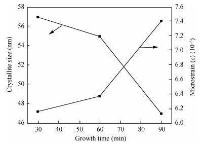
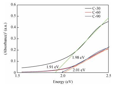
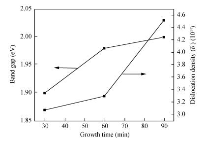
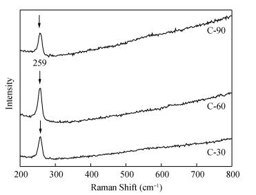
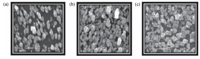
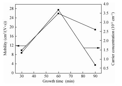
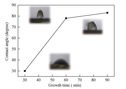
Table 1. Band gap, microstrain, dislocation density, crystallite size (D) and full width half maxima (β) for Cu3Se2 films were measured at various growth time.

|
Table 2.
Electrical properties of Cu

|
| [1] |
Yin Y, Alivisatos A P. Colloidal nanocrystal synthesis and the organic-inorganic interface. Nature, 2005, 437:664 doi: 10.1038/nature04165
|
| [2] |
Peng Z A, Peng X G. Formation of high-quality CdTe, CdSe, and CdS nanocrystals using CdO as precursor. J Am Chem Soc, 2001, 123:183 doi: 10.1021/ja003633m
|
| [3] |
Yoon H, Granata J, Hebert P, et al. Recent advances in highefficiency Ⅲ-Ⅴ multi-junction solar cells for space applications:ultra triple junction qualification. Prog Photovolt Res Appl, 2005, 13:133 doi: 10.1002/(ISSN)1099-159X
|
| [4] |
Auffan M, Rose J, Bottero J Y, et al. Towards a definition of inorganic nanoparticles from an environmental, health and safety perspective nature. Nanotechnology, 2009, 4:634 http://hero.epa.gov/index.cfm?action=search.view&reference_id=199803
|
| [5] |
Brown G F, Wu J. Third generation photovoltaics. Laser Photon, 2009, 3:394 doi: 10.1002/(ISSN)1863-8899
|
| [6] |
Trindade T, O'Brien P, Pickett N L, et al. Nanocrystalline semiconductors:synthesis, properties, and perspectives. Chem Mater. 2001, 13:3843 doi: 10.1021/cm000843p
|
| [7] |
Schaller R D, Klimov V I. High efficiency carrier multiplication in PbSe nanocrystals:implications for solar energy conversion. Phys Rev Lett, 2004, 92:186601 doi: 10.1103/PhysRevLett.92.186601
|
| [8] |
Gracia V M, Nair P K, Nair M T S, et al. Copper selenide thin films by chemical bath deposition. J Cryst Growth, 1999, 203:113 doi: 10.1016/S0022-0248(99)00040-8
|
| [9] |
Riha S C, Johnson D C, Prieto A L, et al. Cu2Se nanoparticles with tunable electronic properties due to a controlled solid-state phase transition driven by copper oxidation and cationic conduction. J Am Chem Soc, 2010, 133:383 https://www.ncbi.nlm.nih.gov/pubmed/21033686/
|
| [10] |
Estrada C A, Nair P K, Nair M T S, et al. Chemical bath deposition of ZnSe and CuSe thin films using N, N-dimethylselenourea. J Electrochem Soc, 1994, 141:802 doi: 10.1149/1.2054814
|
| [11] |
Schafer A, Kouwitz M, Ahlrichs R, et al. Electronic excitation energies in copper selenide clusters. J Chem Phys, 1996, 104:7113 doi: 10.1063/1.471404
|
| [12] |
Hermann A M, Fabick L. Research on polycrystalline thin-film photovoltaic devices. J Cryst Growth, 1983, 61:658 doi: 10.1016/0022-0248(83)90195-1
|
| [13] |
Peranantham P, Jeyachandran Y L, Viswanathan C, et al. The effect of annealing on vacuum-evaporated copper selenide and indium telluride thin films. Mater Charact, 2007, 58:756 doi: 10.1016/j.matchar.2006.11.019
|
| [14] |
Moysiadou A, Koutsikou R, Bouroushian R, et al. Pulse electrodeposition of copper selenide from acidic aqueous baths. Mater Lett, 2015, 139:112 doi: 10.1016/j.matlet.2014.10.036
|
| [15] |
Levy-Clement C, Neumann-Spallart M, Haram S K, et al. Chemical bath deposition of cubic copper (Ⅰ) selenide and its room temperature transformation to the orthorhombic phase. Thin Solid Films, 1997, 302:12 doi: 10.1016/S0040-6090(97)00021-7
|
| [16] |
Lakshmi M, Bindu K, Bini S, et al. Reversible Cu2-xSe↔Cu3Se2 phase transformation in copper selenide thin films prepared by chemical bath deposition. Thin Solid Films, 2001, 386:127 doi: 10.1016/S0040-6090(00)01783-1
|
| [17] |
Mane R S, Kajve S P, Lokhande C D, et al. Studies on p-type copper (Ⅰ) selenide crystalline thin films for hetero-junction solar cells. Vacuum, 2006, 80:631 doi: 10.1016/j.vacuum.2005.08.021
|
| [18] |
Pathan H M, Lokhande C D, Amalnerkar D P, et al. Modified chemical deposition and physico-chemical properties of copper (Ⅰ) selenide thin films. Appl Surf Sci, 2003, 211:48 doi: 10.1016/S0169-4332(03)00046-1
|
| [19] |
Bi H, Zhao W, Sun S, et al. Graphene films decorated with metal sulfide nanoparticles for use as counter electrodes of dyesensitized solar cells. Carbon, 2013, 61:116 doi: 10.1016/j.carbon.2013.04.075
|
| [20] |
Balis N, Dracopoulos V, Bourikas K, et al. Quantum dot sensitized solar cells based on an optimized combination of ZnS, CdS and CdSe with CoS and CuS counter electrodes. Electron Acta, 2013, 9:246 https://www.researchgate.net/profile/Nikolaos_Balis/publication/256698111_Quantum_dot_sensitized_solar_cells_based_on_an_optimized_combination_of_ZnS_CdS_and_CdSe_with_CoS_and_CuS_counter_electrodes/links/56caf62008ae96cdd06f8c2a.pdf?inViewer=0&pdfJsDownload=0&origin=publication_detail
|
| [21] |
Ambade S B, Mane R S, Kale S S, et al. Chemical synthesis of ptype nanocrystalline copper selenide thin films for heterojunction solar cells. Appl Surf Sci, 2006, 253:2123 doi: 10.1016/j.apsusc.2006.04.012
|
| [22] |
Yang J, Zeng J, Yu S, et al. Formation process of CdS nanorods via solvothermal route. Chem Mater, 2000, 12(11):3259 doi: 10.1021/cm0000144
|
| [23] |
Zhan J, Yang X, Wang D, et al. Polymer-controlled growth of CdS nanowires. Adv Mater, 2000, 12:1348 doi: 10.1002/(ISSN)1521-4095
|
| [24] |
Chen Y, Ding J, Guo Y, et al. A facile route to preparation of CdS nanorods. Mater Chem Phys, 2003, 77:734 doi: 10.1016/S0254-0584(02)00136-0
|
| [25] |
Jun Y, Choi J, Cheon J, et al. Shape control of semiconductor and metal oxide nanocrystals through nonhydrolytic colloidal routes. Angew Chem Int Ed, 2006, 45:3414 doi: 10.1002/(ISSN)1521-3773
|
| [26] |
McDonald S A, Konstantatos G, Zhang S, et al. Solutionprocessed PbS quantum dot infrared photodetectors and photovoltaics. Nat Mater, 2005, 4:138 doi: 10.1038/nmat1299
|
| [27] |
Zhou Y, Eck M, Men C, et al. Efficient polymer nanocrystal hybrid solar cells by improved nanocrystal composition. Sol Energy mater sol Cells, 2001, 95:3227 https://www.researchgate.net/publication/241102179_Efficient_Polymer_Nanocrystal_Hybrid_Solar_Cells_by_Improved_Nanocrystal_Composition
|
| [28] |
Thouin L, Vedel J. Electrodeposition and characterization of CulnSe2 thin films. J Electrochem Soc, 1995, 142:2996 doi: 10.1149/1.2048675
|
| [29] |
Souilah M, Lafondn A, GuillotDeudon C, et al. Structural investigation of the Cu2Se-In2Se3-Ga2Se3 phase diagram, X-ray photoemission and optical properties of the Cu1-z(In0.5Ga0.5)1+z/3Se2 compounds. J Solid State Chem, 2010, 183:2274 doi: 10.1016/j.jssc.2010.08.014
|
| [30] |
Panicker M P R, Knaster M, Kroger F A, et al. Cathodic deposition of CdTe from aqueous electrolytes. J Electrochem Soc, 1978, 125:566 doi: 10.1149/1.2131499
|
| [31] |
Yoon S, Yoon T, Lee K S, et al. Nanoparticle-based approach for the formation of CIS solar cells. Sol Energy Mater Sol Cells, 2009, 93:783 doi: 10.1016/j.solmat.2008.09.061
|
| [32] |
Xie Y, Zheng X, Jiang X, et al. Sonochemical synthesis and mechanistic study of copper selenides Cu2-xSe, β-CuSe, and Cu3Se2. Inorg Chem, 2002, 41:387 doi: 10.1021/ic010108v
|
| [33] |
Zhang S Y, Fang C X, Tian Y P, et al. Synthesis and characterization of hexagonal CuSe nanotubes by templating against trigonal Se nanotubes. Cryst Growth Des, 2006, 6:2809 doi: 10.1021/cg0604430
|
| [34] |
Zhang Y, Qiao Z P, Chen X M, et al. Microwave-assisted elemental direct reaction route to nanocrystalline copper chalcogenides CuSe and Cu2Te. J Mater Chem, 2002, 12:2747 doi: 10.1039/b205558a
|
| [35] |
Bakshi M S, Thakur P, Khullar P, et al. Surface activity of highly hydrophobic surfactants and platelike PbSe and CuSe nanoparticles. Cryst Growth Des, 2010, 10:1813 doi: 10.1021/cg901490w
|
| [36] |
Swanepoel R. Determination of the thickness and optical constants of amorphous silicon. J Phys Sci Instrum, 1983, 16:214 http://citeseerx.ist.psu.edu/showciting?cid=2021303
|
| [37] |
Williamson G B, Smallman R C. Dislocation densities in some annealed and cold-worked metals from measurements on the Xray debye-scherrer spectrum. Phil Mag, 1956, 1:34 doi: 10.1080/14786435608238074
|
| [38] |
Astam A, Akaltun Y, Yildirim M, et al. Conversion of SILAR deposited Cu3Se2 thin films to Cu2-xSe by annealing. Mater Lett, 2016, 9:11 https://www.researchgate.net/profile/Aykut_Astam/publication/286511957_Conversion_of_SILAR_deposited_Cu3Se2_thin_films_to_Cu2-xSe_by_annealing/links/5670374308aececfd55312e1.pdf?origin=publication_list
|
| [39] |
Filippo E, Manno D, Serra A, et al. Synthesis and growth mechanism of dendritic Cu2-xSe microstructures. J Alloys Compd, 2012, 538:8 doi: 10.1016/j.jallcom.2012.05.111
|
| [40] |
Ishii M, Shibata K, Nozaki H, et al. Anion distributions and phase transitions in CuS1-xSex(x=0-1) studied by Raman spectroscopy. J Solid State Chem, 1993, 105:504 doi: 10.1006/jssc.1993.1242
|
| [41] |
Waykar R, Pawbake A, Kulkarni R, et al. Low substrate temperature deposition of transparent and conducting ZnO:Al thin films by RF magnetron sputtering. J Semicond, 2016, 37(4):043001 doi: 10.1088/1674-4926/37/4/043001
|
| [42] |
Benramache S, Chabane F, Benhaoua B, et al. Influence of growth time on crystalline structure, conductivity and optical properties of ZnO thin films. J Semicond, 2013, 34(2):023001 doi: 10.1088/1674-4926/34/2/023001
|
| [43] |
Yadav A A. Nanocrystalline copper selenide thin films by chemical spray pyrolysis. J Mater Sci:Mater Electron, 2014, 5:1251 doi: 10.1007/s10854-014-1717-5
|


Article views: 6068 Times PDF downloads: 43 Times Cited by: 0 Times
Received: 24 October 2016 Revised: 01 December 2016 Online: Published: 01 June 2017
| Citation: |
Balasaheb M. Palve, Sandesh R. Jadkar, Habib M. Pathan. A simple chemical route to synthesize the umangite phase of copper selenide (Cu3Se2) thin film at room temperature[J]. Journal of Semiconductors, 2017, 38(6): 063003. doi: 10.1088/1674-4926/38/6/063003
****
B M Palve, S R Jadkar, H M Pathan. A simple chemical route to synthesize the umangite phase of copper selenide (Cu3Se2) thin film at room temperature[J]. J. Semicond., 2017, 38(6): 063003. doi: 10.1088/1674-4926/38/6/063003.

|
| [1] |
Yin Y, Alivisatos A P. Colloidal nanocrystal synthesis and the organic-inorganic interface. Nature, 2005, 437:664 doi: 10.1038/nature04165
|
| [2] |
Peng Z A, Peng X G. Formation of high-quality CdTe, CdSe, and CdS nanocrystals using CdO as precursor. J Am Chem Soc, 2001, 123:183 doi: 10.1021/ja003633m
|
| [3] |
Yoon H, Granata J, Hebert P, et al. Recent advances in highefficiency Ⅲ-Ⅴ multi-junction solar cells for space applications:ultra triple junction qualification. Prog Photovolt Res Appl, 2005, 13:133 doi: 10.1002/(ISSN)1099-159X
|
| [4] |
Auffan M, Rose J, Bottero J Y, et al. Towards a definition of inorganic nanoparticles from an environmental, health and safety perspective nature. Nanotechnology, 2009, 4:634 http://hero.epa.gov/index.cfm?action=search.view&reference_id=199803
|
| [5] |
Brown G F, Wu J. Third generation photovoltaics. Laser Photon, 2009, 3:394 doi: 10.1002/(ISSN)1863-8899
|
| [6] |
Trindade T, O'Brien P, Pickett N L, et al. Nanocrystalline semiconductors:synthesis, properties, and perspectives. Chem Mater. 2001, 13:3843 doi: 10.1021/cm000843p
|
| [7] |
Schaller R D, Klimov V I. High efficiency carrier multiplication in PbSe nanocrystals:implications for solar energy conversion. Phys Rev Lett, 2004, 92:186601 doi: 10.1103/PhysRevLett.92.186601
|
| [8] |
Gracia V M, Nair P K, Nair M T S, et al. Copper selenide thin films by chemical bath deposition. J Cryst Growth, 1999, 203:113 doi: 10.1016/S0022-0248(99)00040-8
|
| [9] |
Riha S C, Johnson D C, Prieto A L, et al. Cu2Se nanoparticles with tunable electronic properties due to a controlled solid-state phase transition driven by copper oxidation and cationic conduction. J Am Chem Soc, 2010, 133:383 https://www.ncbi.nlm.nih.gov/pubmed/21033686/
|
| [10] |
Estrada C A, Nair P K, Nair M T S, et al. Chemical bath deposition of ZnSe and CuSe thin films using N, N-dimethylselenourea. J Electrochem Soc, 1994, 141:802 doi: 10.1149/1.2054814
|
| [11] |
Schafer A, Kouwitz M, Ahlrichs R, et al. Electronic excitation energies in copper selenide clusters. J Chem Phys, 1996, 104:7113 doi: 10.1063/1.471404
|
| [12] |
Hermann A M, Fabick L. Research on polycrystalline thin-film photovoltaic devices. J Cryst Growth, 1983, 61:658 doi: 10.1016/0022-0248(83)90195-1
|
| [13] |
Peranantham P, Jeyachandran Y L, Viswanathan C, et al. The effect of annealing on vacuum-evaporated copper selenide and indium telluride thin films. Mater Charact, 2007, 58:756 doi: 10.1016/j.matchar.2006.11.019
|
| [14] |
Moysiadou A, Koutsikou R, Bouroushian R, et al. Pulse electrodeposition of copper selenide from acidic aqueous baths. Mater Lett, 2015, 139:112 doi: 10.1016/j.matlet.2014.10.036
|
| [15] |
Levy-Clement C, Neumann-Spallart M, Haram S K, et al. Chemical bath deposition of cubic copper (Ⅰ) selenide and its room temperature transformation to the orthorhombic phase. Thin Solid Films, 1997, 302:12 doi: 10.1016/S0040-6090(97)00021-7
|
| [16] |
Lakshmi M, Bindu K, Bini S, et al. Reversible Cu2-xSe↔Cu3Se2 phase transformation in copper selenide thin films prepared by chemical bath deposition. Thin Solid Films, 2001, 386:127 doi: 10.1016/S0040-6090(00)01783-1
|
| [17] |
Mane R S, Kajve S P, Lokhande C D, et al. Studies on p-type copper (Ⅰ) selenide crystalline thin films for hetero-junction solar cells. Vacuum, 2006, 80:631 doi: 10.1016/j.vacuum.2005.08.021
|
| [18] |
Pathan H M, Lokhande C D, Amalnerkar D P, et al. Modified chemical deposition and physico-chemical properties of copper (Ⅰ) selenide thin films. Appl Surf Sci, 2003, 211:48 doi: 10.1016/S0169-4332(03)00046-1
|
| [19] |
Bi H, Zhao W, Sun S, et al. Graphene films decorated with metal sulfide nanoparticles for use as counter electrodes of dyesensitized solar cells. Carbon, 2013, 61:116 doi: 10.1016/j.carbon.2013.04.075
|
| [20] |
Balis N, Dracopoulos V, Bourikas K, et al. Quantum dot sensitized solar cells based on an optimized combination of ZnS, CdS and CdSe with CoS and CuS counter electrodes. Electron Acta, 2013, 9:246 https://www.researchgate.net/profile/Nikolaos_Balis/publication/256698111_Quantum_dot_sensitized_solar_cells_based_on_an_optimized_combination_of_ZnS_CdS_and_CdSe_with_CoS_and_CuS_counter_electrodes/links/56caf62008ae96cdd06f8c2a.pdf?inViewer=0&pdfJsDownload=0&origin=publication_detail
|
| [21] |
Ambade S B, Mane R S, Kale S S, et al. Chemical synthesis of ptype nanocrystalline copper selenide thin films for heterojunction solar cells. Appl Surf Sci, 2006, 253:2123 doi: 10.1016/j.apsusc.2006.04.012
|
| [22] |
Yang J, Zeng J, Yu S, et al. Formation process of CdS nanorods via solvothermal route. Chem Mater, 2000, 12(11):3259 doi: 10.1021/cm0000144
|
| [23] |
Zhan J, Yang X, Wang D, et al. Polymer-controlled growth of CdS nanowires. Adv Mater, 2000, 12:1348 doi: 10.1002/(ISSN)1521-4095
|
| [24] |
Chen Y, Ding J, Guo Y, et al. A facile route to preparation of CdS nanorods. Mater Chem Phys, 2003, 77:734 doi: 10.1016/S0254-0584(02)00136-0
|
| [25] |
Jun Y, Choi J, Cheon J, et al. Shape control of semiconductor and metal oxide nanocrystals through nonhydrolytic colloidal routes. Angew Chem Int Ed, 2006, 45:3414 doi: 10.1002/(ISSN)1521-3773
|
| [26] |
McDonald S A, Konstantatos G, Zhang S, et al. Solutionprocessed PbS quantum dot infrared photodetectors and photovoltaics. Nat Mater, 2005, 4:138 doi: 10.1038/nmat1299
|
| [27] |
Zhou Y, Eck M, Men C, et al. Efficient polymer nanocrystal hybrid solar cells by improved nanocrystal composition. Sol Energy mater sol Cells, 2001, 95:3227 https://www.researchgate.net/publication/241102179_Efficient_Polymer_Nanocrystal_Hybrid_Solar_Cells_by_Improved_Nanocrystal_Composition
|
| [28] |
Thouin L, Vedel J. Electrodeposition and characterization of CulnSe2 thin films. J Electrochem Soc, 1995, 142:2996 doi: 10.1149/1.2048675
|
| [29] |
Souilah M, Lafondn A, GuillotDeudon C, et al. Structural investigation of the Cu2Se-In2Se3-Ga2Se3 phase diagram, X-ray photoemission and optical properties of the Cu1-z(In0.5Ga0.5)1+z/3Se2 compounds. J Solid State Chem, 2010, 183:2274 doi: 10.1016/j.jssc.2010.08.014
|
| [30] |
Panicker M P R, Knaster M, Kroger F A, et al. Cathodic deposition of CdTe from aqueous electrolytes. J Electrochem Soc, 1978, 125:566 doi: 10.1149/1.2131499
|
| [31] |
Yoon S, Yoon T, Lee K S, et al. Nanoparticle-based approach for the formation of CIS solar cells. Sol Energy Mater Sol Cells, 2009, 93:783 doi: 10.1016/j.solmat.2008.09.061
|
| [32] |
Xie Y, Zheng X, Jiang X, et al. Sonochemical synthesis and mechanistic study of copper selenides Cu2-xSe, β-CuSe, and Cu3Se2. Inorg Chem, 2002, 41:387 doi: 10.1021/ic010108v
|
| [33] |
Zhang S Y, Fang C X, Tian Y P, et al. Synthesis and characterization of hexagonal CuSe nanotubes by templating against trigonal Se nanotubes. Cryst Growth Des, 2006, 6:2809 doi: 10.1021/cg0604430
|
| [34] |
Zhang Y, Qiao Z P, Chen X M, et al. Microwave-assisted elemental direct reaction route to nanocrystalline copper chalcogenides CuSe and Cu2Te. J Mater Chem, 2002, 12:2747 doi: 10.1039/b205558a
|
| [35] |
Bakshi M S, Thakur P, Khullar P, et al. Surface activity of highly hydrophobic surfactants and platelike PbSe and CuSe nanoparticles. Cryst Growth Des, 2010, 10:1813 doi: 10.1021/cg901490w
|
| [36] |
Swanepoel R. Determination of the thickness and optical constants of amorphous silicon. J Phys Sci Instrum, 1983, 16:214 http://citeseerx.ist.psu.edu/showciting?cid=2021303
|
| [37] |
Williamson G B, Smallman R C. Dislocation densities in some annealed and cold-worked metals from measurements on the Xray debye-scherrer spectrum. Phil Mag, 1956, 1:34 doi: 10.1080/14786435608238074
|
| [38] |
Astam A, Akaltun Y, Yildirim M, et al. Conversion of SILAR deposited Cu3Se2 thin films to Cu2-xSe by annealing. Mater Lett, 2016, 9:11 https://www.researchgate.net/profile/Aykut_Astam/publication/286511957_Conversion_of_SILAR_deposited_Cu3Se2_thin_films_to_Cu2-xSe_by_annealing/links/5670374308aececfd55312e1.pdf?origin=publication_list
|
| [39] |
Filippo E, Manno D, Serra A, et al. Synthesis and growth mechanism of dendritic Cu2-xSe microstructures. J Alloys Compd, 2012, 538:8 doi: 10.1016/j.jallcom.2012.05.111
|
| [40] |
Ishii M, Shibata K, Nozaki H, et al. Anion distributions and phase transitions in CuS1-xSex(x=0-1) studied by Raman spectroscopy. J Solid State Chem, 1993, 105:504 doi: 10.1006/jssc.1993.1242
|
| [41] |
Waykar R, Pawbake A, Kulkarni R, et al. Low substrate temperature deposition of transparent and conducting ZnO:Al thin films by RF magnetron sputtering. J Semicond, 2016, 37(4):043001 doi: 10.1088/1674-4926/37/4/043001
|
| [42] |
Benramache S, Chabane F, Benhaoua B, et al. Influence of growth time on crystalline structure, conductivity and optical properties of ZnO thin films. J Semicond, 2013, 34(2):023001 doi: 10.1088/1674-4926/34/2/023001
|
| [43] |
Yadav A A. Nanocrystalline copper selenide thin films by chemical spray pyrolysis. J Mater Sci:Mater Electron, 2014, 5:1251 doi: 10.1007/s10854-014-1717-5
|

 WeChat ID
Journal of Semiconductors © 2017 All Rights Reserved 京ICP备05085259号-2

 DownLoad:

