


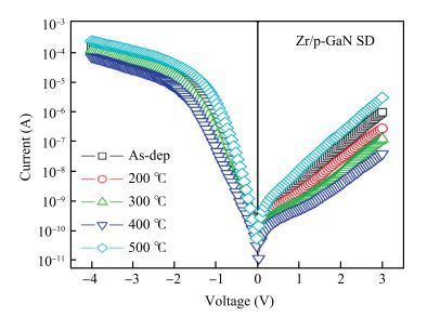
Fig. 1.
(Color online) Reverse and forward current-voltage (I-V) characteristics of the Zr/p-GaN Schottky diode at different annealing temperatures.
SEMICONDUCTOR DEVICES
V. Rajagopal Reddy1, , B. Asha1 and Chel-Jong Choi2,
Corresponding author: V. Rajagopal Reddy Email:vrg@rediffmail.com; Chel-Jong Choi Email:cjchoi@chonbuk.ac.kr
Abstract: The Schottky barrier junction parameters and structural properties of Zr/p-GaN Schottky diode are explored at various annealing temperatures. Experimental analysis showed that the barrier height (BH) of the Zr/pGaN Schottky diode increases with annealing at 400℃ (0.92 eV (I-V)/1.09 eV (C-V)compared to the asdeposited one (0.83 eV (I-V)/0.93 eV (C-V). However, the BH decreases after annealing at 500℃. Also, at different annealing temperatures, the series resistance and BH are assessed by Cheung's functions and their values compared. Further, the interface state density (NSS)of the diode decreases after annealing at 400℃ and then somewhat rises upon annealing at 500℃. Analysis reveals that the maximum BH is obtained at 400℃, and thus the optimum annealing temperature is 400℃ for the diode. The XPS and XRD analysis revealed that the increase in BH may be attributed to the creation of Zr-N phases with increasing annealing up to 400℃. The BH reduces for the diode annealed at 500℃, which may be due to the formation of Ga-Zr phases at the junction. The AFM measurements reveal that the overall surface roughness of the Zr film is quite smooth during rapid annealing process.
Keywords: zirconium Schottky contacts, p-type GaN, electrical characteristics, energy distribution curves, X-ray photoelectron spectroscopy, X-ray diffraction
| [1] |
Chen L C, Hsu C Y, Lan W H, et al. GaN-based light-emitting diodes with Ni/AuBe transparent conductive layer. Solid State Electron, 2003, 47:1843 doi: 10.1016/S0038-1101(03)00129-1
|
| [2] |
Huang L H, Yeh S H, Lee C T, et al. AlGaN/GaN metal-oxidesemiconductor high-electron mobility transistors using oxide insulator grown by photoelectrochemical oxidation method. IEEE Electron Devices Lett, 2008, 29:284 doi: 10.1109/LED.2008.917326
|
| [3] |
Miyajima T, Watanabe H, Ikeda M, et al. Picosecond optical pulse generation from self-pulsating bisectional GaN-based blue-violet laser diodes. Appl Phys Lett, 2009, 94:161103 doi: 10.1063/1.3106055
|
| [4] |
Ravinandan M, Koteswara Rao P, Rajagopal Reddy V. Analysis of the current-voltage characteristics of the Pd/Au Schottky structure on n-type GaN in a wide temperature range. Semicond Sci Technol, 2009, 24:035004 doi: 10.1088/0268-1242/24/3/035004
|
| [5] |
Kim T K, Kim S H, Yang S S, et al. GaN-based light-emitting diode with textured indium tin oxide transparent layer coated with Al2O3 powder. Appl Phys Lett, 2009, 94:161107 doi: 10.1063/1.3120222
|
| [6] |
Takahashi K, Ao J P, Ikawa Y, et al. GaN Schottky diodes for microwave power rectification. Jpn J Appl Phys, 2009, 48:04C095 doi: 10.1143/JJAP.48.04C095/pdf
|
| [7] |
Hu W D, Chen X S, Yin F, et al. Two-dimensional transient simulations of drain lag and current collapse in GaN-based high-electron-mobility transistors. J Appl Phys, 2009, 105:084502 doi: 10.1063/1.3106603
|
| [8] |
Korona K P, Drabinska A, Caban P, et al. Tunable GaN/AlGaN ultraviolet detectors with built-in electric field. J Appl Phys, 2009, 105:083712 doi: 10.1063/1.3110106
|
| [9] |
Chen Z, Pei Y, Newman S, et al. Growth of AlGaN/GaN heterojunction field effect transistors on semi-insulating GaN using an AlGaN interlayer. Appl Phys Lett, 2009, 94:112108 doi: 10.1063/1.3103210
|
| [10] |
Lin J C, Su Y K, Chang S J, et al. High responsivity of GaN p-i-np-i-n photodiode by using low-temperature interlayer. Appl Phys Lett, 2007, 91:173502 doi: 10.1063/1.2800813
|
| [11] |
Wu J. When group-Ⅲ nitrides go infrared:new properties and perspectives. J Appl Phys, 2009, 106:011101 doi: 10.1063/1.3155798
|
| [12] |
Yu L S, Qiao D, Jia L, et al. Study of Schottky barrier of Ni on p-GaN. Appl Phys Lett, 2001, 97:4536 doi: 10.1063/1.1428773
|
| [13] |
Kim J W, Lee J W. Ti/Al p-GaN Schottky barrier height determined by C -V measurements. Appl Surf Sci, 2005, 250:247 doi: 10.1016/j.apsusc.2005.01.004
|
| [14] |
Tan C K, Abdul Aziz A, Yam F K. Schottky barrier properties of various metal (Zr, Ti, Cr, Pt) contact on p-GaN revealed from I -V -T measurement. Appl Surf Sci, 2006, 252:5930 doi: 10.1016/j.apsusc.2005.08.018
|
| [15] |
Fukushima Y, Ogisu K, Kuzuhara M, et al. I -V and C -V characteristics of rare-earth-metal/p-GaN Schottky contacts. Phys Status Solidi C, 2009, 6:S856 doi: 10.1002/pssc.v6.5s2
|
| [16] |
Jang S H, Jang J S. Electrical characteristics and carrier transport mechanism for Ti/p-GaN Schottky diodes. Electron Mater Lett, 2013, 9:245 doi: 10.1007/s13391-012-2175-y
|
| [17] |
Nagaraju G, Dasaradha Rao L, Rajagopal Reddy V. Annealing effects on the electrical, structural and morphological properties of Ti/p-GaN/Ni/Au Schottky diode. Appl Phys A, 2015, 121:131 https://www.researchgate.net/profile/Dasaradha_Lambada/publication/280624228_Annealing_effects_on_the_electrical_structural_and_morphological_properties_of_Tip-GaNNiAu_Schottky_diode/links/55bf844f08aed621de139800.pdf
|
| [18] |
Padma R, Nagaraju G, Rajagopal R V, et al. Effect of annealing temperature on the electrical and structural properties of V/pGaN Schottky structures. Thin Solid Films, 2016, 598:236 doi: 10.1016/j.tsf.2015.12.018
|
| [19] |
Aoki T, Tanikawa T, Katayama R, et al. Electrical characteristics of N-polar (000T) p-type GaN Schottky contacts. Jpn J Appl Phys, 2016, 55:04EJ09 doi: 10.7567/JJAP.55.04EJ09/pdf
|
| [20] |
Rajagopal Reddy V, Asha B, Choi C J. Effects of annealing on electrical characteristics and current transport mechanisms of the Y/p-GaN Schottky diode. J Electron Mater, 2016, 45:3268 doi: 10.1007/s11664-016-4490-9
|
| [21] |
Rhoderick E H, Williams R H. Metal-semiconductor contacts. Oxford:Clarendon, 1988
|
| [22] |
Altindal S, Karadeniz S, Tugluoglu N, et al. The role of interface states and series resistance on the I -V and C -V characteristics in Al/SnO2/p-Si Schottky diodes. Solid State Electron, 2003, 47:1847 doi: 10.1016/S0038-1101(03)00182-5
|
| [23] |
Tung R T. Electron transport at metal-semiconductor interfaces:general theory. Phys Rev B, 1992, 45:13509 doi: 10.1103/PhysRevB.45.13509
|
| [24] |
Sze S M. Physics of semiconductor devices. 2nd ed. New York:Willey, 1981
|
| [25] |
Cheung S K, Cheung N W. Extraction of Schottky diode parameters from forward current-voltage characteristics. Appl Phys Lett, 1986, 49:85 doi: 10.1063/1.97359
|
| [26] |
Mohan G D. Fluctuations in Schottky barrier heights. J Appl Phys, 1984, 55:980 doi: 10.1063/1.333153
|
| [27] |
Song Y P, Van Meirhaeghe R L, Laflere W H, et al. On the difference in apparent barrier height as obtained from capacitancevoltage and current-voltage-temperature measurements on Al/pInP Schottky barriers. Solid State Electron, 1986, 29:633 doi: 10.1016/0038-1101(86)90145-0
|
| [28] |
Werner J H, Guttler H H. Barrier inhomogeneities at Schottky contacts. J Appl Phys, 1991, 69:1522 doi: 10.1063/1.347243
|
| [29] |
Boyarbay B, Cetin H, Kaya M, et al. Correlation between barrier heights and ideality factors of H-terminated Sn/p-Si(100) Schottky barrier diodes. Microelectron Eng, 2008, 85:721 doi: 10.1016/j.mee.2008.01.005
|
| [30] |
Geng L, Ponce F A, Tanaka S, et al. Surface morphology of AlxGa1-xN films grown by MOCVD. Phys Stat Sol A, 2001, 188:803 doi: 10.1002/(ISSN)1521-396X
|
| [31] |
Card H C, Rhoderick E H. Studies of tunnel MOS diodes Ⅱ. thermal equilibrium considerations. J Phys D Appl Phys, 1971, 4:1589 doi: 10.1088/0022-3727/4/10/319
|
| [32] |
Rajagopal Reddy V. Electrical properties and conduction mechanism of an organic-modified Au/NiPc/n-InP Schottky barrier diode. Appl Phys A, 2014, 116:1379 doi: 10.1007/s00339-014-8238-1
|
| [33] |
Karatas S, Altindal S, Turut A, et al. Temperature dependence of characteristic parameters of the H-terminated Sn/p-Si(100) Schottky contacts. Appl Surf Sci, 2003, 217:250 doi: 10.1016/S0169-4332(03)00564-6
|
| [34] |
Karatas S, Turut A. The determination of electronic and interface state density distributions of Au/n-type GaAs Schottky barrier diodes. Physica B, 2006, 381:199 doi: 10.1016/j.physb.2006.01.412
|
| [35] |
Prasanna Lakshmi B, Rajagopal Reddy V, Janardhanam V, et al. Effect of annealing temperature on the electrical properties of Au/Ta2O5/n-GaN metal-insulator-semiconductor (MIS) structure. Appl Phys A, 2013, 113:713 doi: 10.1007/s00339-013-7797-x
|
| [36] |
Monch W. Semiconductor surfaces and interfaces. 3rd ed. Berlin:Springer, 2001
|
| [37] |
Huang T S, Fang R S. Barrier height enhancement of Pt/n-InP Schottky diodes by P2S5/(NH4)2S solution treatment of the InP surface. Solid State Electron, 1994, 37:1461 doi: 10.1016/0038-1101(94)90152-X
|
| [38] |
Guo J D, Pan F M, Feng M S, et al. Schottky contact and the thermal stability of Ni on n-type GaN. J Appl Phys, 1996, 80:1623 doi: 10.1063/1.363822
|
| [39] |
Rajagopal Reddy V, Koteswara Rao P. Annealing temperature effect on electrical and structural properties of Cu/Au Schottky contacts to n-type GaN. Microelectron Eng, 2008, 85:470 doi: 10.1016/j.mee.2007.08.006
|
| [40] |
Siva Pratap Reddy M, Rajagopal Reddy V, Choi C J. Electrical properties and interfacial reactions of rapidly annealed Ni/Ru Schottky rectifiers on n-type GaN. J Alloys Compd, 2010, 503:186 doi: 10.1016/j.jallcom.2010.04.230
|
| [41] |
Jyothi I, Rajagopal Reddy V, Choi C J. Microstructural and electrical characteristics of rapidly annealed Ni/Mo Schottky rectifiers on cleaned n-type GaN (0001) surface. J Mater Sci Mater Electron, 2011, 22:286 doi: 10.1007/s10854-010-0129-4
|
| [42] |
Nanda Kumar Reddy N, Rajagopal Reddy V, Choi C J. Influence of rapid thermal annealing effect on electrical and structural properties of Pd/Ru Schottky contacts to n-type GaN. Mater Chem Phys, 2011, 130:1000 doi: 10.1016/j.matchemphys.2011.08.026
|
| [43] |
Wang J, Zhao D G, Sun Y P, et al. Thermal annealing behaviour of Pt on n-GaN Schottky contacts. J Phys D Appl Phys, 2003, 36:1018 doi: 10.1088/0022-3727/36/8/312
|
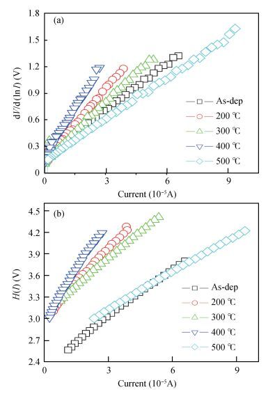
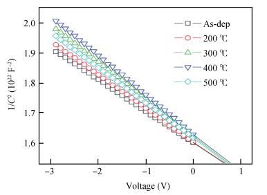
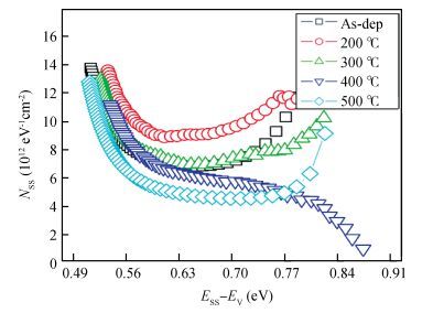
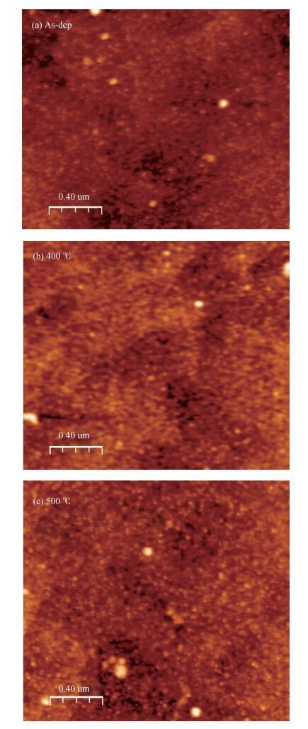
Table 1. Review on different Schottky contacts on p-GaN.
 |
Table 2. The calculated barrier height, ideality factor, series resistance and interface state density of the Zr/p-GaN Schottky diode by I-V and C-V techniques at different annealing temperatures.
 |
| [1] |
Chen L C, Hsu C Y, Lan W H, et al. GaN-based light-emitting diodes with Ni/AuBe transparent conductive layer. Solid State Electron, 2003, 47:1843 doi: 10.1016/S0038-1101(03)00129-1
|
| [2] |
Huang L H, Yeh S H, Lee C T, et al. AlGaN/GaN metal-oxidesemiconductor high-electron mobility transistors using oxide insulator grown by photoelectrochemical oxidation method. IEEE Electron Devices Lett, 2008, 29:284 doi: 10.1109/LED.2008.917326
|
| [3] |
Miyajima T, Watanabe H, Ikeda M, et al. Picosecond optical pulse generation from self-pulsating bisectional GaN-based blue-violet laser diodes. Appl Phys Lett, 2009, 94:161103 doi: 10.1063/1.3106055
|
| [4] |
Ravinandan M, Koteswara Rao P, Rajagopal Reddy V. Analysis of the current-voltage characteristics of the Pd/Au Schottky structure on n-type GaN in a wide temperature range. Semicond Sci Technol, 2009, 24:035004 doi: 10.1088/0268-1242/24/3/035004
|
| [5] |
Kim T K, Kim S H, Yang S S, et al. GaN-based light-emitting diode with textured indium tin oxide transparent layer coated with Al2O3 powder. Appl Phys Lett, 2009, 94:161107 doi: 10.1063/1.3120222
|
| [6] |
Takahashi K, Ao J P, Ikawa Y, et al. GaN Schottky diodes for microwave power rectification. Jpn J Appl Phys, 2009, 48:04C095 doi: 10.1143/JJAP.48.04C095/pdf
|
| [7] |
Hu W D, Chen X S, Yin F, et al. Two-dimensional transient simulations of drain lag and current collapse in GaN-based high-electron-mobility transistors. J Appl Phys, 2009, 105:084502 doi: 10.1063/1.3106603
|
| [8] |
Korona K P, Drabinska A, Caban P, et al. Tunable GaN/AlGaN ultraviolet detectors with built-in electric field. J Appl Phys, 2009, 105:083712 doi: 10.1063/1.3110106
|
| [9] |
Chen Z, Pei Y, Newman S, et al. Growth of AlGaN/GaN heterojunction field effect transistors on semi-insulating GaN using an AlGaN interlayer. Appl Phys Lett, 2009, 94:112108 doi: 10.1063/1.3103210
|
| [10] |
Lin J C, Su Y K, Chang S J, et al. High responsivity of GaN p-i-np-i-n photodiode by using low-temperature interlayer. Appl Phys Lett, 2007, 91:173502 doi: 10.1063/1.2800813
|
| [11] |
Wu J. When group-Ⅲ nitrides go infrared:new properties and perspectives. J Appl Phys, 2009, 106:011101 doi: 10.1063/1.3155798
|
| [12] |
Yu L S, Qiao D, Jia L, et al. Study of Schottky barrier of Ni on p-GaN. Appl Phys Lett, 2001, 97:4536 doi: 10.1063/1.1428773
|
| [13] |
Kim J W, Lee J W. Ti/Al p-GaN Schottky barrier height determined by C -V measurements. Appl Surf Sci, 2005, 250:247 doi: 10.1016/j.apsusc.2005.01.004
|
| [14] |
Tan C K, Abdul Aziz A, Yam F K. Schottky barrier properties of various metal (Zr, Ti, Cr, Pt) contact on p-GaN revealed from I -V -T measurement. Appl Surf Sci, 2006, 252:5930 doi: 10.1016/j.apsusc.2005.08.018
|
| [15] |
Fukushima Y, Ogisu K, Kuzuhara M, et al. I -V and C -V characteristics of rare-earth-metal/p-GaN Schottky contacts. Phys Status Solidi C, 2009, 6:S856 doi: 10.1002/pssc.v6.5s2
|
| [16] |
Jang S H, Jang J S. Electrical characteristics and carrier transport mechanism for Ti/p-GaN Schottky diodes. Electron Mater Lett, 2013, 9:245 doi: 10.1007/s13391-012-2175-y
|
| [17] |
Nagaraju G, Dasaradha Rao L, Rajagopal Reddy V. Annealing effects on the electrical, structural and morphological properties of Ti/p-GaN/Ni/Au Schottky diode. Appl Phys A, 2015, 121:131 https://www.researchgate.net/profile/Dasaradha_Lambada/publication/280624228_Annealing_effects_on_the_electrical_structural_and_morphological_properties_of_Tip-GaNNiAu_Schottky_diode/links/55bf844f08aed621de139800.pdf
|
| [18] |
Padma R, Nagaraju G, Rajagopal R V, et al. Effect of annealing temperature on the electrical and structural properties of V/pGaN Schottky structures. Thin Solid Films, 2016, 598:236 doi: 10.1016/j.tsf.2015.12.018
|
| [19] |
Aoki T, Tanikawa T, Katayama R, et al. Electrical characteristics of N-polar (000T) p-type GaN Schottky contacts. Jpn J Appl Phys, 2016, 55:04EJ09 doi: 10.7567/JJAP.55.04EJ09/pdf
|
| [20] |
Rajagopal Reddy V, Asha B, Choi C J. Effects of annealing on electrical characteristics and current transport mechanisms of the Y/p-GaN Schottky diode. J Electron Mater, 2016, 45:3268 doi: 10.1007/s11664-016-4490-9
|
| [21] |
Rhoderick E H, Williams R H. Metal-semiconductor contacts. Oxford:Clarendon, 1988
|
| [22] |
Altindal S, Karadeniz S, Tugluoglu N, et al. The role of interface states and series resistance on the I -V and C -V characteristics in Al/SnO2/p-Si Schottky diodes. Solid State Electron, 2003, 47:1847 doi: 10.1016/S0038-1101(03)00182-5
|
| [23] |
Tung R T. Electron transport at metal-semiconductor interfaces:general theory. Phys Rev B, 1992, 45:13509 doi: 10.1103/PhysRevB.45.13509
|
| [24] |
Sze S M. Physics of semiconductor devices. 2nd ed. New York:Willey, 1981
|
| [25] |
Cheung S K, Cheung N W. Extraction of Schottky diode parameters from forward current-voltage characteristics. Appl Phys Lett, 1986, 49:85 doi: 10.1063/1.97359
|
| [26] |
Mohan G D. Fluctuations in Schottky barrier heights. J Appl Phys, 1984, 55:980 doi: 10.1063/1.333153
|
| [27] |
Song Y P, Van Meirhaeghe R L, Laflere W H, et al. On the difference in apparent barrier height as obtained from capacitancevoltage and current-voltage-temperature measurements on Al/pInP Schottky barriers. Solid State Electron, 1986, 29:633 doi: 10.1016/0038-1101(86)90145-0
|
| [28] |
Werner J H, Guttler H H. Barrier inhomogeneities at Schottky contacts. J Appl Phys, 1991, 69:1522 doi: 10.1063/1.347243
|
| [29] |
Boyarbay B, Cetin H, Kaya M, et al. Correlation between barrier heights and ideality factors of H-terminated Sn/p-Si(100) Schottky barrier diodes. Microelectron Eng, 2008, 85:721 doi: 10.1016/j.mee.2008.01.005
|
| [30] |
Geng L, Ponce F A, Tanaka S, et al. Surface morphology of AlxGa1-xN films grown by MOCVD. Phys Stat Sol A, 2001, 188:803 doi: 10.1002/(ISSN)1521-396X
|
| [31] |
Card H C, Rhoderick E H. Studies of tunnel MOS diodes Ⅱ. thermal equilibrium considerations. J Phys D Appl Phys, 1971, 4:1589 doi: 10.1088/0022-3727/4/10/319
|
| [32] |
Rajagopal Reddy V. Electrical properties and conduction mechanism of an organic-modified Au/NiPc/n-InP Schottky barrier diode. Appl Phys A, 2014, 116:1379 doi: 10.1007/s00339-014-8238-1
|
| [33] |
Karatas S, Altindal S, Turut A, et al. Temperature dependence of characteristic parameters of the H-terminated Sn/p-Si(100) Schottky contacts. Appl Surf Sci, 2003, 217:250 doi: 10.1016/S0169-4332(03)00564-6
|
| [34] |
Karatas S, Turut A. The determination of electronic and interface state density distributions of Au/n-type GaAs Schottky barrier diodes. Physica B, 2006, 381:199 doi: 10.1016/j.physb.2006.01.412
|
| [35] |
Prasanna Lakshmi B, Rajagopal Reddy V, Janardhanam V, et al. Effect of annealing temperature on the electrical properties of Au/Ta2O5/n-GaN metal-insulator-semiconductor (MIS) structure. Appl Phys A, 2013, 113:713 doi: 10.1007/s00339-013-7797-x
|
| [36] |
Monch W. Semiconductor surfaces and interfaces. 3rd ed. Berlin:Springer, 2001
|
| [37] |
Huang T S, Fang R S. Barrier height enhancement of Pt/n-InP Schottky diodes by P2S5/(NH4)2S solution treatment of the InP surface. Solid State Electron, 1994, 37:1461 doi: 10.1016/0038-1101(94)90152-X
|
| [38] |
Guo J D, Pan F M, Feng M S, et al. Schottky contact and the thermal stability of Ni on n-type GaN. J Appl Phys, 1996, 80:1623 doi: 10.1063/1.363822
|
| [39] |
Rajagopal Reddy V, Koteswara Rao P. Annealing temperature effect on electrical and structural properties of Cu/Au Schottky contacts to n-type GaN. Microelectron Eng, 2008, 85:470 doi: 10.1016/j.mee.2007.08.006
|
| [40] |
Siva Pratap Reddy M, Rajagopal Reddy V, Choi C J. Electrical properties and interfacial reactions of rapidly annealed Ni/Ru Schottky rectifiers on n-type GaN. J Alloys Compd, 2010, 503:186 doi: 10.1016/j.jallcom.2010.04.230
|
| [41] |
Jyothi I, Rajagopal Reddy V, Choi C J. Microstructural and electrical characteristics of rapidly annealed Ni/Mo Schottky rectifiers on cleaned n-type GaN (0001) surface. J Mater Sci Mater Electron, 2011, 22:286 doi: 10.1007/s10854-010-0129-4
|
| [42] |
Nanda Kumar Reddy N, Rajagopal Reddy V, Choi C J. Influence of rapid thermal annealing effect on electrical and structural properties of Pd/Ru Schottky contacts to n-type GaN. Mater Chem Phys, 2011, 130:1000 doi: 10.1016/j.matchemphys.2011.08.026
|
| [43] |
Wang J, Zhao D G, Sun Y P, et al. Thermal annealing behaviour of Pt on n-GaN Schottky contacts. J Phys D Appl Phys, 2003, 36:1018 doi: 10.1088/0022-3727/36/8/312
|


Article views: 5817 Times PDF downloads: 121 Times Cited by: 0 Times
Received: 06 November 2016 Revised: 06 December 2016 Online: Published: 01 June 2017
| Citation: |
V. Rajagopal Reddy, B. Asha, Chel-Jong Choi. Schottky barrier parameters and structural properties of rapidly annealed Zr Schottky electrode on p-type GaN[J]. Journal of Semiconductors, 2017, 38(6): 064001. doi: 10.1088/1674-4926/38/6/064001
****
V R Reddy, B Asha, C J Choi. Schottky barrier parameters and structural properties of rapidly annealed Zr Schottky electrode on p-type GaN[J]. J. Semicond., 2017, 38(6): 064001. doi: 10.1088/1674-4926/38/6/064001.

|
| [1] |
Chen L C, Hsu C Y, Lan W H, et al. GaN-based light-emitting diodes with Ni/AuBe transparent conductive layer. Solid State Electron, 2003, 47:1843 doi: 10.1016/S0038-1101(03)00129-1
|
| [2] |
Huang L H, Yeh S H, Lee C T, et al. AlGaN/GaN metal-oxidesemiconductor high-electron mobility transistors using oxide insulator grown by photoelectrochemical oxidation method. IEEE Electron Devices Lett, 2008, 29:284 doi: 10.1109/LED.2008.917326
|
| [3] |
Miyajima T, Watanabe H, Ikeda M, et al. Picosecond optical pulse generation from self-pulsating bisectional GaN-based blue-violet laser diodes. Appl Phys Lett, 2009, 94:161103 doi: 10.1063/1.3106055
|
| [4] |
Ravinandan M, Koteswara Rao P, Rajagopal Reddy V. Analysis of the current-voltage characteristics of the Pd/Au Schottky structure on n-type GaN in a wide temperature range. Semicond Sci Technol, 2009, 24:035004 doi: 10.1088/0268-1242/24/3/035004
|
| [5] |
Kim T K, Kim S H, Yang S S, et al. GaN-based light-emitting diode with textured indium tin oxide transparent layer coated with Al2O3 powder. Appl Phys Lett, 2009, 94:161107 doi: 10.1063/1.3120222
|
| [6] |
Takahashi K, Ao J P, Ikawa Y, et al. GaN Schottky diodes for microwave power rectification. Jpn J Appl Phys, 2009, 48:04C095 doi: 10.1143/JJAP.48.04C095/pdf
|
| [7] |
Hu W D, Chen X S, Yin F, et al. Two-dimensional transient simulations of drain lag and current collapse in GaN-based high-electron-mobility transistors. J Appl Phys, 2009, 105:084502 doi: 10.1063/1.3106603
|
| [8] |
Korona K P, Drabinska A, Caban P, et al. Tunable GaN/AlGaN ultraviolet detectors with built-in electric field. J Appl Phys, 2009, 105:083712 doi: 10.1063/1.3110106
|
| [9] |
Chen Z, Pei Y, Newman S, et al. Growth of AlGaN/GaN heterojunction field effect transistors on semi-insulating GaN using an AlGaN interlayer. Appl Phys Lett, 2009, 94:112108 doi: 10.1063/1.3103210
|
| [10] |
Lin J C, Su Y K, Chang S J, et al. High responsivity of GaN p-i-np-i-n photodiode by using low-temperature interlayer. Appl Phys Lett, 2007, 91:173502 doi: 10.1063/1.2800813
|
| [11] |
Wu J. When group-Ⅲ nitrides go infrared:new properties and perspectives. J Appl Phys, 2009, 106:011101 doi: 10.1063/1.3155798
|
| [12] |
Yu L S, Qiao D, Jia L, et al. Study of Schottky barrier of Ni on p-GaN. Appl Phys Lett, 2001, 97:4536 doi: 10.1063/1.1428773
|
| [13] |
Kim J W, Lee J W. Ti/Al p-GaN Schottky barrier height determined by C -V measurements. Appl Surf Sci, 2005, 250:247 doi: 10.1016/j.apsusc.2005.01.004
|
| [14] |
Tan C K, Abdul Aziz A, Yam F K. Schottky barrier properties of various metal (Zr, Ti, Cr, Pt) contact on p-GaN revealed from I -V -T measurement. Appl Surf Sci, 2006, 252:5930 doi: 10.1016/j.apsusc.2005.08.018
|
| [15] |
Fukushima Y, Ogisu K, Kuzuhara M, et al. I -V and C -V characteristics of rare-earth-metal/p-GaN Schottky contacts. Phys Status Solidi C, 2009, 6:S856 doi: 10.1002/pssc.v6.5s2
|
| [16] |
Jang S H, Jang J S. Electrical characteristics and carrier transport mechanism for Ti/p-GaN Schottky diodes. Electron Mater Lett, 2013, 9:245 doi: 10.1007/s13391-012-2175-y
|
| [17] |
Nagaraju G, Dasaradha Rao L, Rajagopal Reddy V. Annealing effects on the electrical, structural and morphological properties of Ti/p-GaN/Ni/Au Schottky diode. Appl Phys A, 2015, 121:131 https://www.researchgate.net/profile/Dasaradha_Lambada/publication/280624228_Annealing_effects_on_the_electrical_structural_and_morphological_properties_of_Tip-GaNNiAu_Schottky_diode/links/55bf844f08aed621de139800.pdf
|
| [18] |
Padma R, Nagaraju G, Rajagopal R V, et al. Effect of annealing temperature on the electrical and structural properties of V/pGaN Schottky structures. Thin Solid Films, 2016, 598:236 doi: 10.1016/j.tsf.2015.12.018
|
| [19] |
Aoki T, Tanikawa T, Katayama R, et al. Electrical characteristics of N-polar (000T) p-type GaN Schottky contacts. Jpn J Appl Phys, 2016, 55:04EJ09 doi: 10.7567/JJAP.55.04EJ09/pdf
|
| [20] |
Rajagopal Reddy V, Asha B, Choi C J. Effects of annealing on electrical characteristics and current transport mechanisms of the Y/p-GaN Schottky diode. J Electron Mater, 2016, 45:3268 doi: 10.1007/s11664-016-4490-9
|
| [21] |
Rhoderick E H, Williams R H. Metal-semiconductor contacts. Oxford:Clarendon, 1988
|
| [22] |
Altindal S, Karadeniz S, Tugluoglu N, et al. The role of interface states and series resistance on the I -V and C -V characteristics in Al/SnO2/p-Si Schottky diodes. Solid State Electron, 2003, 47:1847 doi: 10.1016/S0038-1101(03)00182-5
|
| [23] |
Tung R T. Electron transport at metal-semiconductor interfaces:general theory. Phys Rev B, 1992, 45:13509 doi: 10.1103/PhysRevB.45.13509
|
| [24] |
Sze S M. Physics of semiconductor devices. 2nd ed. New York:Willey, 1981
|
| [25] |
Cheung S K, Cheung N W. Extraction of Schottky diode parameters from forward current-voltage characteristics. Appl Phys Lett, 1986, 49:85 doi: 10.1063/1.97359
|
| [26] |
Mohan G D. Fluctuations in Schottky barrier heights. J Appl Phys, 1984, 55:980 doi: 10.1063/1.333153
|
| [27] |
Song Y P, Van Meirhaeghe R L, Laflere W H, et al. On the difference in apparent barrier height as obtained from capacitancevoltage and current-voltage-temperature measurements on Al/pInP Schottky barriers. Solid State Electron, 1986, 29:633 doi: 10.1016/0038-1101(86)90145-0
|
| [28] |
Werner J H, Guttler H H. Barrier inhomogeneities at Schottky contacts. J Appl Phys, 1991, 69:1522 doi: 10.1063/1.347243
|
| [29] |
Boyarbay B, Cetin H, Kaya M, et al. Correlation between barrier heights and ideality factors of H-terminated Sn/p-Si(100) Schottky barrier diodes. Microelectron Eng, 2008, 85:721 doi: 10.1016/j.mee.2008.01.005
|
| [30] |
Geng L, Ponce F A, Tanaka S, et al. Surface morphology of AlxGa1-xN films grown by MOCVD. Phys Stat Sol A, 2001, 188:803 doi: 10.1002/(ISSN)1521-396X
|
| [31] |
Card H C, Rhoderick E H. Studies of tunnel MOS diodes Ⅱ. thermal equilibrium considerations. J Phys D Appl Phys, 1971, 4:1589 doi: 10.1088/0022-3727/4/10/319
|
| [32] |
Rajagopal Reddy V. Electrical properties and conduction mechanism of an organic-modified Au/NiPc/n-InP Schottky barrier diode. Appl Phys A, 2014, 116:1379 doi: 10.1007/s00339-014-8238-1
|
| [33] |
Karatas S, Altindal S, Turut A, et al. Temperature dependence of characteristic parameters of the H-terminated Sn/p-Si(100) Schottky contacts. Appl Surf Sci, 2003, 217:250 doi: 10.1016/S0169-4332(03)00564-6
|
| [34] |
Karatas S, Turut A. The determination of electronic and interface state density distributions of Au/n-type GaAs Schottky barrier diodes. Physica B, 2006, 381:199 doi: 10.1016/j.physb.2006.01.412
|
| [35] |
Prasanna Lakshmi B, Rajagopal Reddy V, Janardhanam V, et al. Effect of annealing temperature on the electrical properties of Au/Ta2O5/n-GaN metal-insulator-semiconductor (MIS) structure. Appl Phys A, 2013, 113:713 doi: 10.1007/s00339-013-7797-x
|
| [36] |
Monch W. Semiconductor surfaces and interfaces. 3rd ed. Berlin:Springer, 2001
|
| [37] |
Huang T S, Fang R S. Barrier height enhancement of Pt/n-InP Schottky diodes by P2S5/(NH4)2S solution treatment of the InP surface. Solid State Electron, 1994, 37:1461 doi: 10.1016/0038-1101(94)90152-X
|
| [38] |
Guo J D, Pan F M, Feng M S, et al. Schottky contact and the thermal stability of Ni on n-type GaN. J Appl Phys, 1996, 80:1623 doi: 10.1063/1.363822
|
| [39] |
Rajagopal Reddy V, Koteswara Rao P. Annealing temperature effect on electrical and structural properties of Cu/Au Schottky contacts to n-type GaN. Microelectron Eng, 2008, 85:470 doi: 10.1016/j.mee.2007.08.006
|
| [40] |
Siva Pratap Reddy M, Rajagopal Reddy V, Choi C J. Electrical properties and interfacial reactions of rapidly annealed Ni/Ru Schottky rectifiers on n-type GaN. J Alloys Compd, 2010, 503:186 doi: 10.1016/j.jallcom.2010.04.230
|
| [41] |
Jyothi I, Rajagopal Reddy V, Choi C J. Microstructural and electrical characteristics of rapidly annealed Ni/Mo Schottky rectifiers on cleaned n-type GaN (0001) surface. J Mater Sci Mater Electron, 2011, 22:286 doi: 10.1007/s10854-010-0129-4
|
| [42] |
Nanda Kumar Reddy N, Rajagopal Reddy V, Choi C J. Influence of rapid thermal annealing effect on electrical and structural properties of Pd/Ru Schottky contacts to n-type GaN. Mater Chem Phys, 2011, 130:1000 doi: 10.1016/j.matchemphys.2011.08.026
|
| [43] |
Wang J, Zhao D G, Sun Y P, et al. Thermal annealing behaviour of Pt on n-GaN Schottky contacts. J Phys D Appl Phys, 2003, 36:1018 doi: 10.1088/0022-3727/36/8/312
|

 WeChat ID
Journal of Semiconductors © 2017 All Rights Reserved 京ICP备05085259号-2

 DownLoad:

