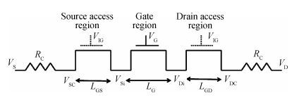
Fig. 1.
(Color online) Cross sectional view of p-GaN gate AlGaN/GaN HEMT.
SEMICONDUCTOR DEVICES
D.K. Panda and T.R. Lenka
Corresponding author: T. R. Lenka Email:t.r.lenka@ieee.org
Abstract: An enhancement mode p-GaN gate AlGaN/GaN HEMT is proposed and a physics based virtual source charge model with Landauer approach for electron transport has been developed using Verilog-A and simulated using Cadence Spectre, in order to predict device characteristics such as threshold voltage, drain current and gate capacitance. The drain current model incorporates important physical effects such as velocity saturation, short channel effects like DIBL (drain induced barrier lowering), channel length modulation (CLM), and mobility degradation due to self-heating. The predicted Id-Vds, Id-Vgs, and C-V characteristics show an excellent agreement with the experimental data for both drain current and capacitance which validate the model. The developed model was then utilized to design and simulate a single-pole single-throw (SPST) RF switch.
| [1] |
Lenka T R, Panda A K. AlGaN/GaN-based HEMT on SiCsubstrate for microwave characteristics using different passivation layers. Pramana-J Phys, 2012, 79(1):151 doi: 10.1007/s12043-012-0290-9
|
| [2] |
Lenka T R, Panda A K. Self-consistent subband calculations of AlxGa1-xN/(AlN)/GaN-based high electron mobility transistor. Adv Mater Res, 2011, 159:342
|
| [3] |
Swain R, Jena K, Lenka T R. Oxide interfacial charge engineering towards normally-off AlN/GaN MOSHEMT. Mater Sci Semicond Process, 2016, 53:66 doi: 10.1016/j.mssp.2016.06.008
|
| [4] |
Swain R, Jena K, Lenka T R. Interface DOS dependent analytical model development for DC characteristics of normally-off AlN/GaN MOSHEMT. Superlattices Microstruct, 2015, 84:54 doi: 10.1016/j.spmi.2015.04.025
|
| [5] |
Endoh A, Yamashita Y, Ikeda K, et al. Non-recessed-gate enhancement-mode AlGaN/GaN high electron mobility transistors with high RF performance. Jpn J Appl Phys, 2004, 43(4B):2255 doi: 10.1143/JJAP.43.2255
|
| [6] |
Im K S, Kim R H, Kim K W, et al. Normally off singlenanoribbon Al2O3/GaN MISFET. IEEE Electron Device Lett, 2012, 34(1):27
|
| [7] |
Cai Y, Zhou Y, Lau K M, et al. Control of threshold voltage of AlGaN/GaN HEMTs by fluoride-based plasma treatment:from depletion mode to enhancement mode. IEEE Trans Electron Devices, 2006, 53(9):2207 doi: 10.1109/TED.2006.881054
|
| [8] |
Hu X, Simin G, Yang J, et al. Enhancement mode AlGaN/GaN HFET with selectively grown pn junction gate. Electron Lett, 2000, 36(8):753 doi: 10.1049/el:20000557
|
| [9] |
Maeda N, Hiroki M, Sasaki S, et al. High-temperature characteristics in normally off AlGaN/GaN heterostructure field-effect transistors with recessed-gate enhanced-barrier structures. Appl Phys Express, 2012, 5(8):084201 doi: 10.1143/APEX.5.084201
|
| [10] |
Tsuyukuchi N, Nagamatsu K, Hirose Y, et al. Low-leakagecurrent enhancement-mode AlGaN/GaN heterostructure fieldeffect transistor using p-type gate contact. Jpn J Appl Phys, 2006, 45(8-11):319 doi: 10.1143/JJAP.45.L319/pdf
|
| [11] |
Hwang I, Choi H, Lee J, et al. 1.6 kV, 2.9 mΩ cm2 normally-off p-GaN HEMT device. 24th International Symposium on Power Semiconductor Devices and ICs, Bruges, 2012:41
|
| [12] |
Katsuno T, Kanechika M, Itoh K, et al. Improvement of current collapse by surface treatment and passivation layer in p-GaN gate GaN high-electron-mobility transistors. Jpn J Appl Phys, 2013, 52(4):04CF08 https://www.researchgate.net/publication/272992586_Improvement_of_Current_Collapse_by_Surface_Treatment_and_Passivation_Layer_in_p-GaN_Gate_GaN_High-Electron-Mobility_Transistors
|
| [13] |
Hwang I, Kim J, Choi H S, et al. p-GaN gate HEMTs with tungsten gate metal for high threshold voltage and low gate current. IEEE Electron Device Lett, 2013, 34(2):202 doi: 10.1109/LED.2012.2230312
|
| [14] |
Khakifirooz A, Nayfeh O M, Antoniadis D, et al. A simple semiempirical short-channel MOSFET current-voltage model continuous across all regions of operation and employing only physical parameters. IEEE Trans Electron Devices, 2009, 56(8):1674 doi: 10.1109/TED.2009.2024022
|
| [15] |
Tsividis Y, McAndrew C. Operation and modeling of the MOS transistor. Oxford University Press, 2011
|
| [16] |
Caughey D M, Thomas R E. Carrier mobilities in silicon empirically related to doping and field. Proc IEEE, 1967, 55(12):2192 doi: 10.1109/PROC.1967.6123
|
| [17] |
Radhakrishna U, Piedra D, Zhang Y H, et al. High voltage GaN HEMT compact model:experimental verification, field plate optimization and charge trapping. IEEE Int Electron Devices Meeting, Washington, DC, 2013, 32.7.1 https://www.researchgate.net/publication/271482613_High_voltage_GaN_HEMT_compact_model_Experimental_verification_field_plate_optimization_and_charge_trapping
|
| [18] |
Khandelwal S, Yadav C, Agnihotri S, et al. Robust surfacepotential-based compact model for GaN HEMT IC design. IEEE Trans Electron Devices, 2013, 60(10):3216 doi: 10.1109/TED.2013.2265320
|
| [19] |
Deng W, Huang J, Ma X Y, et al. An explicit surface potential calculation and compact current model for AlGaN/GaN HEMTs. IEEE Electron Device Lett, 2015, 36(2):108 doi: 10.1109/LED.2015.2388706
|
| [20] |
Lee F, Su L Y, Wang C H, et al. Impact of gate metal on the performance of p-GaN/AlGaN/GaN high electron mobility transistors. IEEE Electron Device Lett, 2015, 36(3):232 doi: 10.1109/LED.2015.2395454
|
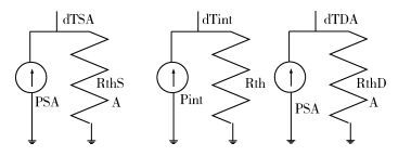
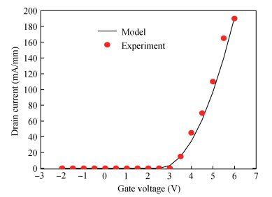

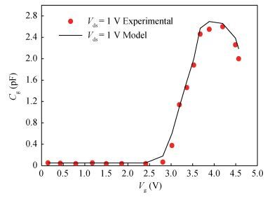
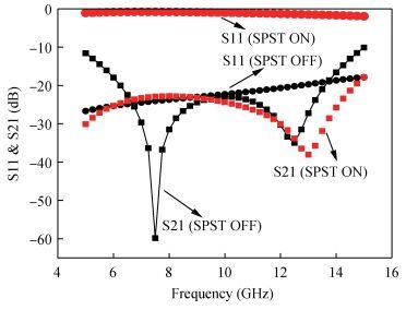
Table 1. Summary of extracted device and model parameters.
 |
| [1] |
Lenka T R, Panda A K. AlGaN/GaN-based HEMT on SiCsubstrate for microwave characteristics using different passivation layers. Pramana-J Phys, 2012, 79(1):151 doi: 10.1007/s12043-012-0290-9
|
| [2] |
Lenka T R, Panda A K. Self-consistent subband calculations of AlxGa1-xN/(AlN)/GaN-based high electron mobility transistor. Adv Mater Res, 2011, 159:342
|
| [3] |
Swain R, Jena K, Lenka T R. Oxide interfacial charge engineering towards normally-off AlN/GaN MOSHEMT. Mater Sci Semicond Process, 2016, 53:66 doi: 10.1016/j.mssp.2016.06.008
|
| [4] |
Swain R, Jena K, Lenka T R. Interface DOS dependent analytical model development for DC characteristics of normally-off AlN/GaN MOSHEMT. Superlattices Microstruct, 2015, 84:54 doi: 10.1016/j.spmi.2015.04.025
|
| [5] |
Endoh A, Yamashita Y, Ikeda K, et al. Non-recessed-gate enhancement-mode AlGaN/GaN high electron mobility transistors with high RF performance. Jpn J Appl Phys, 2004, 43(4B):2255 doi: 10.1143/JJAP.43.2255
|
| [6] |
Im K S, Kim R H, Kim K W, et al. Normally off singlenanoribbon Al2O3/GaN MISFET. IEEE Electron Device Lett, 2012, 34(1):27
|
| [7] |
Cai Y, Zhou Y, Lau K M, et al. Control of threshold voltage of AlGaN/GaN HEMTs by fluoride-based plasma treatment:from depletion mode to enhancement mode. IEEE Trans Electron Devices, 2006, 53(9):2207 doi: 10.1109/TED.2006.881054
|
| [8] |
Hu X, Simin G, Yang J, et al. Enhancement mode AlGaN/GaN HFET with selectively grown pn junction gate. Electron Lett, 2000, 36(8):753 doi: 10.1049/el:20000557
|
| [9] |
Maeda N, Hiroki M, Sasaki S, et al. High-temperature characteristics in normally off AlGaN/GaN heterostructure field-effect transistors with recessed-gate enhanced-barrier structures. Appl Phys Express, 2012, 5(8):084201 doi: 10.1143/APEX.5.084201
|
| [10] |
Tsuyukuchi N, Nagamatsu K, Hirose Y, et al. Low-leakagecurrent enhancement-mode AlGaN/GaN heterostructure fieldeffect transistor using p-type gate contact. Jpn J Appl Phys, 2006, 45(8-11):319 doi: 10.1143/JJAP.45.L319/pdf
|
| [11] |
Hwang I, Choi H, Lee J, et al. 1.6 kV, 2.9 mΩ cm2 normally-off p-GaN HEMT device. 24th International Symposium on Power Semiconductor Devices and ICs, Bruges, 2012:41
|
| [12] |
Katsuno T, Kanechika M, Itoh K, et al. Improvement of current collapse by surface treatment and passivation layer in p-GaN gate GaN high-electron-mobility transistors. Jpn J Appl Phys, 2013, 52(4):04CF08 https://www.researchgate.net/publication/272992586_Improvement_of_Current_Collapse_by_Surface_Treatment_and_Passivation_Layer_in_p-GaN_Gate_GaN_High-Electron-Mobility_Transistors
|
| [13] |
Hwang I, Kim J, Choi H S, et al. p-GaN gate HEMTs with tungsten gate metal for high threshold voltage and low gate current. IEEE Electron Device Lett, 2013, 34(2):202 doi: 10.1109/LED.2012.2230312
|
| [14] |
Khakifirooz A, Nayfeh O M, Antoniadis D, et al. A simple semiempirical short-channel MOSFET current-voltage model continuous across all regions of operation and employing only physical parameters. IEEE Trans Electron Devices, 2009, 56(8):1674 doi: 10.1109/TED.2009.2024022
|
| [15] |
Tsividis Y, McAndrew C. Operation and modeling of the MOS transistor. Oxford University Press, 2011
|
| [16] |
Caughey D M, Thomas R E. Carrier mobilities in silicon empirically related to doping and field. Proc IEEE, 1967, 55(12):2192 doi: 10.1109/PROC.1967.6123
|
| [17] |
Radhakrishna U, Piedra D, Zhang Y H, et al. High voltage GaN HEMT compact model:experimental verification, field plate optimization and charge trapping. IEEE Int Electron Devices Meeting, Washington, DC, 2013, 32.7.1 https://www.researchgate.net/publication/271482613_High_voltage_GaN_HEMT_compact_model_Experimental_verification_field_plate_optimization_and_charge_trapping
|
| [18] |
Khandelwal S, Yadav C, Agnihotri S, et al. Robust surfacepotential-based compact model for GaN HEMT IC design. IEEE Trans Electron Devices, 2013, 60(10):3216 doi: 10.1109/TED.2013.2265320
|
| [19] |
Deng W, Huang J, Ma X Y, et al. An explicit surface potential calculation and compact current model for AlGaN/GaN HEMTs. IEEE Electron Device Lett, 2015, 36(2):108 doi: 10.1109/LED.2015.2388706
|
| [20] |
Lee F, Su L Y, Wang C H, et al. Impact of gate metal on the performance of p-GaN/AlGaN/GaN high electron mobility transistors. IEEE Electron Device Lett, 2015, 36(3):232 doi: 10.1109/LED.2015.2395454
|


Article views: 6555 Times PDF downloads: 346 Times Cited by: 0 Times
Received: 22 November 2016 Revised: 25 December 2016 Online: Published: 01 June 2017
| Citation: |
D.K. Panda, T.R. Lenka. Modeling and simulation of enhancement mode p-GaN Gate AlGaN/GaN HEMT for RF circuit switch applications[J]. Journal of Semiconductors, 2017, 38(6): 064002. doi: 10.1088/1674-4926/38/6/064002
****
D.K. Panda, T.R. Lenka. Modeling and simulation of enhancement mode p-GaN Gate AlGaN/GaN HEMT for RF circuit switch applications[J]. J. Semicond., 2017, 38(6): 064002. doi: 10.1088/1674-4926/38/6/064002.

|
| [1] |
Lenka T R, Panda A K. AlGaN/GaN-based HEMT on SiCsubstrate for microwave characteristics using different passivation layers. Pramana-J Phys, 2012, 79(1):151 doi: 10.1007/s12043-012-0290-9
|
| [2] |
Lenka T R, Panda A K. Self-consistent subband calculations of AlxGa1-xN/(AlN)/GaN-based high electron mobility transistor. Adv Mater Res, 2011, 159:342
|
| [3] |
Swain R, Jena K, Lenka T R. Oxide interfacial charge engineering towards normally-off AlN/GaN MOSHEMT. Mater Sci Semicond Process, 2016, 53:66 doi: 10.1016/j.mssp.2016.06.008
|
| [4] |
Swain R, Jena K, Lenka T R. Interface DOS dependent analytical model development for DC characteristics of normally-off AlN/GaN MOSHEMT. Superlattices Microstruct, 2015, 84:54 doi: 10.1016/j.spmi.2015.04.025
|
| [5] |
Endoh A, Yamashita Y, Ikeda K, et al. Non-recessed-gate enhancement-mode AlGaN/GaN high electron mobility transistors with high RF performance. Jpn J Appl Phys, 2004, 43(4B):2255 doi: 10.1143/JJAP.43.2255
|
| [6] |
Im K S, Kim R H, Kim K W, et al. Normally off singlenanoribbon Al2O3/GaN MISFET. IEEE Electron Device Lett, 2012, 34(1):27
|
| [7] |
Cai Y, Zhou Y, Lau K M, et al. Control of threshold voltage of AlGaN/GaN HEMTs by fluoride-based plasma treatment:from depletion mode to enhancement mode. IEEE Trans Electron Devices, 2006, 53(9):2207 doi: 10.1109/TED.2006.881054
|
| [8] |
Hu X, Simin G, Yang J, et al. Enhancement mode AlGaN/GaN HFET with selectively grown pn junction gate. Electron Lett, 2000, 36(8):753 doi: 10.1049/el:20000557
|
| [9] |
Maeda N, Hiroki M, Sasaki S, et al. High-temperature characteristics in normally off AlGaN/GaN heterostructure field-effect transistors with recessed-gate enhanced-barrier structures. Appl Phys Express, 2012, 5(8):084201 doi: 10.1143/APEX.5.084201
|
| [10] |
Tsuyukuchi N, Nagamatsu K, Hirose Y, et al. Low-leakagecurrent enhancement-mode AlGaN/GaN heterostructure fieldeffect transistor using p-type gate contact. Jpn J Appl Phys, 2006, 45(8-11):319 doi: 10.1143/JJAP.45.L319/pdf
|
| [11] |
Hwang I, Choi H, Lee J, et al. 1.6 kV, 2.9 mΩ cm2 normally-off p-GaN HEMT device. 24th International Symposium on Power Semiconductor Devices and ICs, Bruges, 2012:41
|
| [12] |
Katsuno T, Kanechika M, Itoh K, et al. Improvement of current collapse by surface treatment and passivation layer in p-GaN gate GaN high-electron-mobility transistors. Jpn J Appl Phys, 2013, 52(4):04CF08 https://www.researchgate.net/publication/272992586_Improvement_of_Current_Collapse_by_Surface_Treatment_and_Passivation_Layer_in_p-GaN_Gate_GaN_High-Electron-Mobility_Transistors
|
| [13] |
Hwang I, Kim J, Choi H S, et al. p-GaN gate HEMTs with tungsten gate metal for high threshold voltage and low gate current. IEEE Electron Device Lett, 2013, 34(2):202 doi: 10.1109/LED.2012.2230312
|
| [14] |
Khakifirooz A, Nayfeh O M, Antoniadis D, et al. A simple semiempirical short-channel MOSFET current-voltage model continuous across all regions of operation and employing only physical parameters. IEEE Trans Electron Devices, 2009, 56(8):1674 doi: 10.1109/TED.2009.2024022
|
| [15] |
Tsividis Y, McAndrew C. Operation and modeling of the MOS transistor. Oxford University Press, 2011
|
| [16] |
Caughey D M, Thomas R E. Carrier mobilities in silicon empirically related to doping and field. Proc IEEE, 1967, 55(12):2192 doi: 10.1109/PROC.1967.6123
|
| [17] |
Radhakrishna U, Piedra D, Zhang Y H, et al. High voltage GaN HEMT compact model:experimental verification, field plate optimization and charge trapping. IEEE Int Electron Devices Meeting, Washington, DC, 2013, 32.7.1 https://www.researchgate.net/publication/271482613_High_voltage_GaN_HEMT_compact_model_Experimental_verification_field_plate_optimization_and_charge_trapping
|
| [18] |
Khandelwal S, Yadav C, Agnihotri S, et al. Robust surfacepotential-based compact model for GaN HEMT IC design. IEEE Trans Electron Devices, 2013, 60(10):3216 doi: 10.1109/TED.2013.2265320
|
| [19] |
Deng W, Huang J, Ma X Y, et al. An explicit surface potential calculation and compact current model for AlGaN/GaN HEMTs. IEEE Electron Device Lett, 2015, 36(2):108 doi: 10.1109/LED.2015.2388706
|
| [20] |
Lee F, Su L Y, Wang C H, et al. Impact of gate metal on the performance of p-GaN/AlGaN/GaN high electron mobility transistors. IEEE Electron Device Lett, 2015, 36(3):232 doi: 10.1109/LED.2015.2395454
|

 WeChat ID
Journal of Semiconductors © 2017 All Rights Reserved 京ICP备05085259号-2

 DownLoad: