


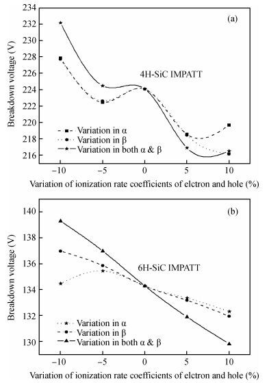
Fig. 1.
Effect on breakdown voltage of 4H-SiC & 6H-SiC IMPATT with the variation of ionization rate coefficient of electron and hole.
SEMICONDUCTOR DEVICES
S K Swain1, J Pradhan2, , G N Dash1 and S R Pattanaik3
Corresponding author: J Pradhan Email:janmejaya74@gmail.com
Abstract: Ionization rate coefficients and saturation drift velocities for electrons and holes are the vital material parameters in determining the performance of an IMPATT diode. We have performed a sensitivity analysis of the millimeter wave characteristics of 4H-SiC and 6H-SiC IMPATT diodes with reference to the above mentioned material data and an operating frequency of 220 GHz. The effect of a small variation in the ionization rate and drift velocity on the device characteristics like break down voltage, efficiency, noise measure and power output has been presented here.
Keywords: IMPATT, SiC, ionization rate, saturation drift velocity, millimeter wave
| [1] |
Pradhan J, Swain S K, Pattanaik S R, et al. Competence of 4H-SiC IMPATT diode for terahertz application. Asian J Phys, 201221(2):175 https://www.researchgate.net/publication/261062242_Competence_of_4H-SiC_IMPATT_Diode_for_Terahertz_Application
|
| [2] |
Panda A K, Pavlidis D, Alekseev E. DC and high-frequency characteristics of GaN-based IMPATTs. IEEE Trans Electron Devices, 2001, 48(4):820 doi: 10.1109/16.915735
|
| [3] |
Zhao J H, Gruzinskis V, Luo Y, et al. Monte Carlo simulation of 4H-SiC IMPATT diode. Semicond Sci Technol, 2000, 15(11):1093 doi: 10.1088/0268-1242/15/11/314
|
| [4] |
Pradhan J, Pattanaik S R, Swain S K, et al. Low noise wide bandgap SiC based IMPATT diodes at sub-millimeter wave frequencies and at high temperature. J Semicond, 2014, 35(3):034006 doi: 10.1088/1674-4926/35/3/034006
|
| [5] |
Mukherjee M, Mazumder N, Roy S K. Photosensitivity analysis of gallium nitride and silicon carbide terahertz IMPATT oscillators:comparison of theoretical reliability and study on experimental feasibility. IEEE Trans Device Mater Reliab, 2008, (8):608 http://ieeexplore.ieee.org/xpls/abs_all.jsp?isnumber=4655569&arnumber=4595636
|
| [6] |
Pradhan J, Swain S K, Pattanaik S R, et al. Identification of electron and hole ionization rates in GaAs with reference to IMPATT Diode. IOSR J Appl Phys, 2012, 2(1):24 doi: 10.9790/4861
|
| [7] |
Pattanaik S R, Pradhan J, Swain S K, et al. Influence of small variation on impact ionization rate data on simulation 4H-SiC IMPATT. Int Soc Opt Photonics, 2011:8549B-6 https://www.researchgate.net/publication/271483957_Influence_of_small_variation_in_impact_ionization_rate_data_on_simulation_of_4H-SiC_IMPATT
|
| [8] |
Yuan L, Cooper J A, Melloch M R Jr, et al. Experimental demonstration of a SiC IMPATT Oscillator. IEEE Electron Devices Lett, 2001, 22:266 doi: 10.1109/55.924837
|
| [9] |
Pattanaik S R, Dash G N, Mishra J K. Prospects of 6H-SiC for operation as an IMPATT Diode at 140 GHz. Semicond Sci Technol, 2005, 20(3):299 doi: 10.1088/0268-1242/20/3/008
|
| [10] |
Mukherjee M, Mazumder N, Roy S K.α-SiC nanoscale transittime diodes:performance of the photo-irradiated terahertz sourcesatelevatedtemperature.SemicondSciTechnol, 2010, 25:055008 doi: 10.1088/0268-1242/25/5/055008/pdf
|
| [11] |
Konstantinov A O, Wahab Q, Nordell N, et al. Ionization rates and critical fields in 4H silicon carbide. Appl Phys Lett, 1997, 71(1):90 doi: 10.1063/1.119478
|
| [12] |
Raghunathan R, Baliga B J. Temperature dependence of hole impact ionization coefficients in 4H and 6H-SiC. Solid State Electron 1999, 43(2):199 doi: 10.1016/S0038-1101(98)00248-2
|
| [13] |
Khan I A, Cooper J A Jr. Measurement of high field electron transport in silicon carbide. IEEE Trans Electron Devices, 2000, 47:269 doi: 10.1109/16.822266
|
| [14] |
Electronic archive: New Semiconductor Materials, Characteristics and Properties[online], Available: http://www.ioffe.ru/SVA/NSM/Semicond/SiC/
|
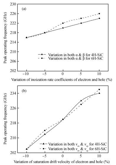
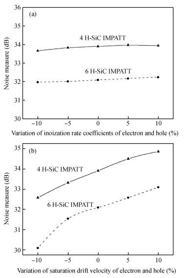
Table 1. Design parameters of 6H-SiC and 4H-SiC DDR at 220 GHz.
 |
Table 2. Millimeter wave characteristics of SiC DDR IMPATT diodes at 220 GHz.
 |
| [1] |
Pradhan J, Swain S K, Pattanaik S R, et al. Competence of 4H-SiC IMPATT diode for terahertz application. Asian J Phys, 201221(2):175 https://www.researchgate.net/publication/261062242_Competence_of_4H-SiC_IMPATT_Diode_for_Terahertz_Application
|
| [2] |
Panda A K, Pavlidis D, Alekseev E. DC and high-frequency characteristics of GaN-based IMPATTs. IEEE Trans Electron Devices, 2001, 48(4):820 doi: 10.1109/16.915735
|
| [3] |
Zhao J H, Gruzinskis V, Luo Y, et al. Monte Carlo simulation of 4H-SiC IMPATT diode. Semicond Sci Technol, 2000, 15(11):1093 doi: 10.1088/0268-1242/15/11/314
|
| [4] |
Pradhan J, Pattanaik S R, Swain S K, et al. Low noise wide bandgap SiC based IMPATT diodes at sub-millimeter wave frequencies and at high temperature. J Semicond, 2014, 35(3):034006 doi: 10.1088/1674-4926/35/3/034006
|
| [5] |
Mukherjee M, Mazumder N, Roy S K. Photosensitivity analysis of gallium nitride and silicon carbide terahertz IMPATT oscillators:comparison of theoretical reliability and study on experimental feasibility. IEEE Trans Device Mater Reliab, 2008, (8):608 http://ieeexplore.ieee.org/xpls/abs_all.jsp?isnumber=4655569&arnumber=4595636
|
| [6] |
Pradhan J, Swain S K, Pattanaik S R, et al. Identification of electron and hole ionization rates in GaAs with reference to IMPATT Diode. IOSR J Appl Phys, 2012, 2(1):24 doi: 10.9790/4861
|
| [7] |
Pattanaik S R, Pradhan J, Swain S K, et al. Influence of small variation on impact ionization rate data on simulation 4H-SiC IMPATT. Int Soc Opt Photonics, 2011:8549B-6 https://www.researchgate.net/publication/271483957_Influence_of_small_variation_in_impact_ionization_rate_data_on_simulation_of_4H-SiC_IMPATT
|
| [8] |
Yuan L, Cooper J A, Melloch M R Jr, et al. Experimental demonstration of a SiC IMPATT Oscillator. IEEE Electron Devices Lett, 2001, 22:266 doi: 10.1109/55.924837
|
| [9] |
Pattanaik S R, Dash G N, Mishra J K. Prospects of 6H-SiC for operation as an IMPATT Diode at 140 GHz. Semicond Sci Technol, 2005, 20(3):299 doi: 10.1088/0268-1242/20/3/008
|
| [10] |
Mukherjee M, Mazumder N, Roy S K.α-SiC nanoscale transittime diodes:performance of the photo-irradiated terahertz sourcesatelevatedtemperature.SemicondSciTechnol, 2010, 25:055008 doi: 10.1088/0268-1242/25/5/055008/pdf
|
| [11] |
Konstantinov A O, Wahab Q, Nordell N, et al. Ionization rates and critical fields in 4H silicon carbide. Appl Phys Lett, 1997, 71(1):90 doi: 10.1063/1.119478
|
| [12] |
Raghunathan R, Baliga B J. Temperature dependence of hole impact ionization coefficients in 4H and 6H-SiC. Solid State Electron 1999, 43(2):199 doi: 10.1016/S0038-1101(98)00248-2
|
| [13] |
Khan I A, Cooper J A Jr. Measurement of high field electron transport in silicon carbide. IEEE Trans Electron Devices, 2000, 47:269 doi: 10.1109/16.822266
|
| [14] |
Electronic archive: New Semiconductor Materials, Characteristics and Properties[online], Available: http://www.ioffe.ru/SVA/NSM/Semicond/SiC/
|


Article views: 3596 Times PDF downloads: 22 Times Cited by: 0 Times
Received: 09 July 2016 Revised: 08 October 2016 Online: Published: 01 June 2017
| Citation: |
S K Swain, J Pradhan, G N Dash, S R Pattanaik. A sensitivity analysis of millimeter wave characteristics of SiC IMPATT diodes[J]. Journal of Semiconductors, 2017, 38(6): 064003. doi: 10.1088/1674-4926/38/6/064003
****
S K Swain, J Pradhan, G N Dash, S R Pattanaik. A sensitivity analysis of millimeter wave characteristics of SiC IMPATT diodes[J]. J. Semicond., 2017, 38(6): 064003. doi: 10.1088/1674-4926/38/6/064003.

|
| [1] |
Pradhan J, Swain S K, Pattanaik S R, et al. Competence of 4H-SiC IMPATT diode for terahertz application. Asian J Phys, 201221(2):175 https://www.researchgate.net/publication/261062242_Competence_of_4H-SiC_IMPATT_Diode_for_Terahertz_Application
|
| [2] |
Panda A K, Pavlidis D, Alekseev E. DC and high-frequency characteristics of GaN-based IMPATTs. IEEE Trans Electron Devices, 2001, 48(4):820 doi: 10.1109/16.915735
|
| [3] |
Zhao J H, Gruzinskis V, Luo Y, et al. Monte Carlo simulation of 4H-SiC IMPATT diode. Semicond Sci Technol, 2000, 15(11):1093 doi: 10.1088/0268-1242/15/11/314
|
| [4] |
Pradhan J, Pattanaik S R, Swain S K, et al. Low noise wide bandgap SiC based IMPATT diodes at sub-millimeter wave frequencies and at high temperature. J Semicond, 2014, 35(3):034006 doi: 10.1088/1674-4926/35/3/034006
|
| [5] |
Mukherjee M, Mazumder N, Roy S K. Photosensitivity analysis of gallium nitride and silicon carbide terahertz IMPATT oscillators:comparison of theoretical reliability and study on experimental feasibility. IEEE Trans Device Mater Reliab, 2008, (8):608 http://ieeexplore.ieee.org/xpls/abs_all.jsp?isnumber=4655569&arnumber=4595636
|
| [6] |
Pradhan J, Swain S K, Pattanaik S R, et al. Identification of electron and hole ionization rates in GaAs with reference to IMPATT Diode. IOSR J Appl Phys, 2012, 2(1):24 doi: 10.9790/4861
|
| [7] |
Pattanaik S R, Pradhan J, Swain S K, et al. Influence of small variation on impact ionization rate data on simulation 4H-SiC IMPATT. Int Soc Opt Photonics, 2011:8549B-6 https://www.researchgate.net/publication/271483957_Influence_of_small_variation_in_impact_ionization_rate_data_on_simulation_of_4H-SiC_IMPATT
|
| [8] |
Yuan L, Cooper J A, Melloch M R Jr, et al. Experimental demonstration of a SiC IMPATT Oscillator. IEEE Electron Devices Lett, 2001, 22:266 doi: 10.1109/55.924837
|
| [9] |
Pattanaik S R, Dash G N, Mishra J K. Prospects of 6H-SiC for operation as an IMPATT Diode at 140 GHz. Semicond Sci Technol, 2005, 20(3):299 doi: 10.1088/0268-1242/20/3/008
|
| [10] |
Mukherjee M, Mazumder N, Roy S K.α-SiC nanoscale transittime diodes:performance of the photo-irradiated terahertz sourcesatelevatedtemperature.SemicondSciTechnol, 2010, 25:055008 doi: 10.1088/0268-1242/25/5/055008/pdf
|
| [11] |
Konstantinov A O, Wahab Q, Nordell N, et al. Ionization rates and critical fields in 4H silicon carbide. Appl Phys Lett, 1997, 71(1):90 doi: 10.1063/1.119478
|
| [12] |
Raghunathan R, Baliga B J. Temperature dependence of hole impact ionization coefficients in 4H and 6H-SiC. Solid State Electron 1999, 43(2):199 doi: 10.1016/S0038-1101(98)00248-2
|
| [13] |
Khan I A, Cooper J A Jr. Measurement of high field electron transport in silicon carbide. IEEE Trans Electron Devices, 2000, 47:269 doi: 10.1109/16.822266
|
| [14] |
Electronic archive: New Semiconductor Materials, Characteristics and Properties[online], Available: http://www.ioffe.ru/SVA/NSM/Semicond/SiC/
|

 WeChat ID
Journal of Semiconductors © 2017 All Rights Reserved 京ICP备05085259号-2

 DownLoad:

