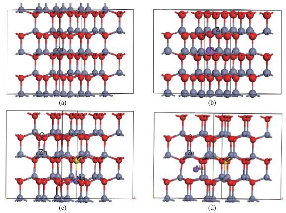
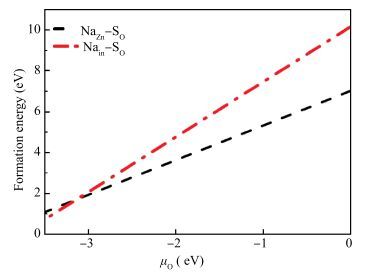
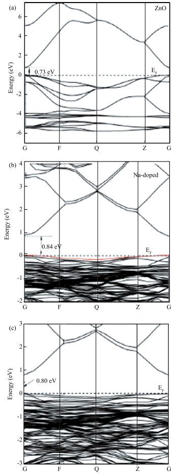
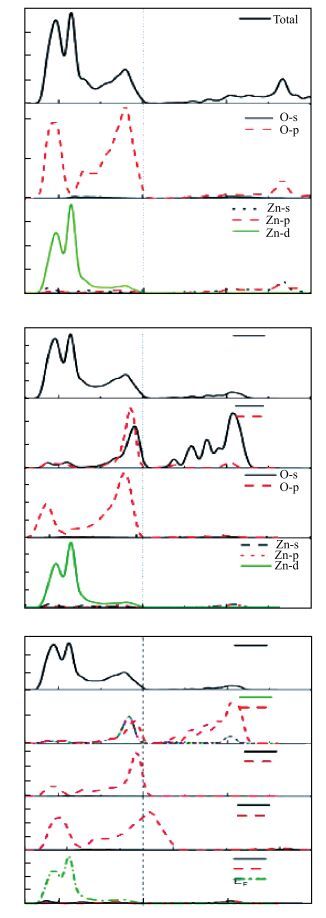
Abstract: Using the first-principles method based on the density functional theory, the formation energy, electronic structures of S-Na co-doping in ZnO were calculated. The calculated results show that NaZn-SO have smaller formation energy than Nain-SO in energy ranges from -3.10 to 0 eV of μO, indicating that it opens up a new opportunity for growth the p-type ZnO. The band structure shows that the NaZn system is a p-type direct-band-gap semiconductor material and the calculated band gap (0.84 eV) is larger than pure ZnO (0.74 eV). The NaZn-SO system is also a p-type semiconductor material with a direct band gap (0.80 eV). The influence of S-Na co-doping in ZnO on p-type conductivity is also discussed. The effective masses of NaZn-SO are larger than effective masses of NaZn and the NaZn-SO have more hole carriers than NaZn, meaning the hole in the NaZn-SO system may have a better carrier transfer character. So we inferred that NaZn-SO should be a candidate of p-type conduction.
Zinc oxide (ZnO) is well known as a fascinating semiconductor with a wide direct band gap of 3.37 eV and a large exciton binding energy of 60 meV at room temperature[1, 2]. The study of ZnO has attracted increasing attention in the past few decades due to its potential applications in short wavelength optoelectronics devices[3-6]. It is well known that both n-type conduction and p-type conduction of ZnO are imperative in optoelectronics devices[7]. However, to date, most ZnO, which exist in nature or have been synthesized in the laboratory, are n-type semiconductors due to the low acceptor solubility, deeper acceptor levels and various self-compensating effect forming native defects[8, 9]. There are a few reports about p-type ZnO[10-15]. Zhang et al.[12] predicted theoretically that Na substitutes Zn in ZnO has a shallow acceptor level on 170 meV. Ye et al.[13, 14] achieved experimentally reliable p-type ZnO thin films and nanorod doped with Na. Recently, Pandey et al.[15] demonstrated reliable fabrication of ZnMgO thin films doped with Na by dual ion beam sputtering, the p-type conduction in thin films has been confirmed by Hall measurement and band structure. In a physical picture, the upper valence band (−4.0 to 0 eV) is contributed mainly by the O-2p orbitals with some mixing of the Zn-3p and Zn-3d orbitals. Thus, Na substitutes for Zn only lead to small perturbations at the valence band maximum (VBM). Furthermore, because the d orbitals of Na do not have any electrons, the weakened p-d coupling also lowers the energy levels[12]. However, it is still difficult to fabricate high-quality p-type ZnO because the Na atoms tend to occupy the interstitial sites, which lead to the self-compensation[8, 9]. On the other hand, Persson et al.[16] reported that the level of VBM of ZnO would shift-up due to a strong valence band offset bowing of S doped in ZnO. The shift-up may lower the acceptor energy level and heighten the doping efficiency of the p-type ZnO. Xu et al.[17] realized p-type conduction in Ag-S codoped ZnO thin films. Yao et al.[18] also observed stable p-type conduction in the Ag-S codoped ZnO thin films, the physical mechanism of this was attributed to the formation of the Ag+Zn-SO complex acceptor. Recently, Niu et al.[19] did an experimental and theoretical research on the S-N co-doped ZnO, and the results show that the S impurity plays a significance role in forming the p-type conductivity. However, to the best of our knowledge, there has been very little research performed on the p-type conduction of Na-S co-doping ZnO. In this work, Na/S mono-doping and Na-S co-doping in ZnO are studied by first-principles calculations, and it is found that Na-S could be a candidate of p-type conduction.
2.
Computational methods
ZnO has a hexagonal structure with a P63mc space group, and each unit cell contains two O atoms and two Zn atoms. In this work, a 72 atoms supercell, which consists of 3 × 3 × 2 primitive cells is used, as shown in Fig. 1(a). Fig. 1(b) shows the Na-doped structure of ZnO (NaZn). For S-Na co-doped structures, we took two configurations into consideration. Fig. 1(c) shows that the Na and S atoms substituted Zn and O atoms, respectively, denoted as NaZn-SO. Fig. 1(d) shows that one S atom substituted an O atom, while the Na atom occupied the interstitial site, denoted by Nain-SO. In the present work, all the structural geometrical optimization, electronic properties are performed using the density function theory (DFT) approach based on pseudo-potential technology. The exchange and correlation interactions were modeled using the generalized gradient approximation (GGA) with the Perdew-Burke-Ernzerhof (PBE) functional[20]. The ionic cores were represented by ultrasoft pseudopotentials for Zn, O, Na and S atoms. The zinc 3d104s2 electrons, the oxygen 2s22p4 electrons, the sulfur 3s23p4electrons and the sodium 2s22p63s1 electrons were treated as a part of the valence states. The Brillouin zone integration was performed over the 3 × 3 × 3 grid sizes using the Monkorst-Pack method, the plane-wave cutoff energy was set as 450 eV. In the structural geometrical optimization processes, the force on each atom was converged to less than 0.1 eV/nm, the maximum ionic displacement was within 0.002 Å, and the total stress tensor was not greater than 0.1 GPa. All the calculations were performed in the reciprocal space.
Figure
1.
(Color online) Supercell of ZnO for (a) ZnO, (b) NaZn, (c) NaZn-SO, and (d) Nain-SO.
The formation energy (Ef) is an important physical factor when it turns to the solubility property and the energy stability of dopants. The formation energy of the doped ZnO supercells in neutral charge state is defined as[21, 22]
Ef[X]=Etot[X]−Etot[bulk]−∑iniμi,
(1)
where Etot[X] is the total energy of the supercell with doping, Etot[bulk] is the total energy of the same supercell without doping, ni is the number of atoms added to (ni>0), or removed out (ni<0) of the supercell, and μi is the chemical potential. We took the two extreme conditions of O-rich and Zn-rich into consideration because the growth environments influence the chemical potential. Under extreme O-rich conditions, μZn=μZn(bulk)+ΔHf, μO=12μO2=12EO2, while extreme Zn-rich conditions, μZn=μZn(bulk)=EZn(bulk),μO=12μO2+ΔHf, where ΔHf is the formation enthalpy of ZnO, and our calculated value (−3.53 eV) is in good agreement with the experimental value of −3.6 eV[23] and the theoretical value of −3.59 eV[24]. Fig. 2 shows the formation energies as a function of μO for NaZn-SO and Nain-SO. According to the results, with increasing μO, it becomes difficult to obtain NaZn-SO and Nain-SO. However, the NaZn-SO have smaller formation energy than Nain-SO in energy ranges from -3.10 to 0 eV of μO, indicating that the density of interstitial impurity of Na is effectively lower using the Na-S co-doping method. This result means a new opportunity for growth of the p-type ZnO has opened up.
Figure
2.
Calculated impurity formation energies as a function of the chemical potential μO for Nain-SOand NaZn-SO.
Fig. 3(a) shows the band structures of pure ZnO. The conduction band minimum and the valence band maximum are at the same G k-point, suggesting a direct gap semiconductor. The calculated band gap (0.74 eV) is smaller than the experimental value (3.37 eV)[1], which is underestimated by GGA, but in good agreement with other calculations using the same method[24]. Figs. 3(b) and 3(c) show the band structures of Na-mono doped ZnO and Na-S codoped ZnO, respectively. The conduction band minimum and the valence band maximum are also at a highly symmetric G k-point, suggesting a direct gap semiconductor. The calculated band gaps are 0.84 eV and 0.80 eV for Na-mono doped ZnO and Na-S codoped ZnO, respectively. The effective hole masses of Na-mono doped ZnO are larger than the effective hole masses of Na-S codoped ZnO because the effective hole masses are proportional to their band gaps based on Zhang's report[25]. Fig. 4(b) displays the total density of states (TDOS) of ZnO, as well as the partial density of states (PDOS) of the Zn and O atoms. It can be observed that the valence band of ZnO can be divided into two parts. The lower valence band (−6.0 to −4.0 eV) is composed mainly of Zn-3d states, the upper valence band (−4.0 to 0 eV) is contributed by O-2p states, in addition, the conduction band is dominated by O-2p and Zn-3d states, which are supported by previous works[26]. The calculated TDOS and PDOS of the Zn, O and Na atoms are plotted in Fig. 4(c). The Fermi level shifts downward into the valence band, exhibiting p-type behavior, and an impurity state is delocalized at the Fermi level. This localized state stems mainly from the O-2p and a small portion of Na-2p states. The localized state from the O-2p is attributed to small perturbations at the valence band maximum. The calculated results demonstrated that p-type ZnO can be obtained by Na-mono doping. The calculated TDOS and PDOS of the Zn, O, S and Na atoms are shown in Fig. 4(c). A similar change trend of Na-mono doped ZnO appeared in Na-S codoped ZnO. The DOS near the Fermi-level increases and originates mainly from O 2p states with a little contribution from Zn 4s, Zn 3p, Zn 3d, Na 2s, Na 2p and S 3p states. It is showed that the contribution to the acceptor level is mainly from Na 2s, Na 2p states and S 3p states. It is therefore illuminated that the level of VBM of ZnO would shift-up due to a strong valence band offset bowing of S doped in ZnO. The shift-up may lower the acceptor energy level and enhance doping efficiency of the p-type ZnO[12]. As a result, p-type ZnO can be achieved by Na-S co-doping. To study the holes generated around the VBM, the areas from the Fermi-levels to the VBMs of Na-mono doped ZnO and Na-S codoped ZnO are integrated. The calculated results are 1.82 and 1.93 for Na-mono doped ZnO and Na-S codoped ZnO, respectively. These results reveal that the Na-S codoped ZnO possesses more hole carriers than Na-mono doped ZnO, which is helpful for p-type ZnO.
Figure
3.
Band structures of ZnO for (a) ZnO, (b) NaZn, (c) NaZn-So.
The calculations regarding the defect formation energies, the electronic structures and the properties of hole carriers of pure, Na-mono, and Na-S co-doped ZnO, were performed using the first-principle method. The calculated results show that NaZn-SO have smaller formation energy than Nain-SOin energy ranges from -3.10 to 0 eV of μO, indicating that it opens up a new opportunity for growth of the p-type ZnO. The Fermi-levels of doped structures moved to lower energy directions, showing p-type conductivities compared to pure ZnO. Subsequent conductivity analyses indicated that Na-S codoped ZnO had a better p-type transportation behavior. We concluded that the Na-S co-doped ZnO structure would be favorable for a p-type ZnO realization.
Acknowledgments:
The calculations were performed at the Center for High Performance Computing of the Northwestern Polytechnical University.
Sara K G, Ramin Y, Farid J S, et al. Optical and electrical properties of p-type Ag-doped ZnO nanostructures. Ceram Int, 2014, 40:7957 doi: 10.1016/j.ceramint.2013.12.145
[3]
Li W J, Kong C Y, Qin G P, et al. p-type conductivity and stability of Ag-N codoped ZnO thin films. J. Alloys Compd, 2014, 609:173 doi: 10.1016/j.jallcom.2014.04.051
[4]
Alivov Y I, Kalinina E V, Cherenkov A E, et al. Fabrication and characterization of n-ZnO/p-AlGaN heterojunction light-emitting diodes on 6H-SiC substrates. Appl Phys Lett, 2003, 83:4719 doi: 10.1063/1.1632537
[5]
Huang Y B, Zhou W, Wu P. Room-temperature ferromagnetism in epitaxial p-type K-doped ZnO films. Solid State Commun, 2014, 183:31 doi: 10.1016/j.ssc.2013.12.024
[6]
Makino T, Chia C H, Tuan N T, et al. Radiative and nonradiative recombination processes in lattice-matched (Cd, Zn)O/(Mg, Zn)O multiquantum wells. Appl Phys Lett, 2000, 77:1632 doi: 10.1063/1.1308540
[7]
Sáaedi A, Yousefi R, Jamali-Sheini F, et al. Optical and electrical properties of p-type Li-doped ZnO nanowires. Superlattices Microstruct, 2013, 61:91 doi: 10.1016/j.spmi.2013.06.014
[8]
Zhang S B, Wei S H, Zunger A. Intrinsic n-type versus p-type doping asymmetry and the defect physics of ZnO. Phys Rev B, 2001, 63:075205 doi: 10.1103/PhysRevB.63.075205
[9]
Dhara S, Giri P K. Stable p-type conductivity and enhanced photoconductivity from nitrogen-doped annealed ZnO thin film. Thin Solid Films, 2012, 520:5000 doi: 10.1016/j.tsf.2012.02.081
[10]
Liu J S, Shan C X, Shen H, et al. ZnO light-emitting devices with a lifetime of 6.8 hours. Appl Phys Lett, 2012, 101:011106 doi: 10.1063/1.4733298
Park C H, Zhang S B, Wei S H. Origin of p-type doping difficulty in ZnO:the impurity perspective. Phys Rev B, 2002, 66:073202 doi: 10.1103/PhysRevB.66.073202
Lin S S, Lu J G, Ye Z Z, et al. p-type behavior in Na-doped ZnO films and ZnO homojunction light-emitting diodes. Solid State Commun, 2008, 148:25 doi: 10.1016/j.ssc.2008.07.028
[15]
Pandey S K, Awasthi V, Sengar B S, et al. Band alignment and photon extraction studies of Na-doped MgZnO/Ga-doped ZnO heterojunction for light-emitter applications. J Appl Phys, 2015, 118:165301 doi: 10.1063/1.4934560
[16]
Persson C, Platzer-Björkman C, Malmström J, et al. Strong valence-band offset bowing of ZnO1-xSx enhances p-type nitrogen doping of ZnO-like alloys. Phys Rev Lett, 2006, 97:146403 doi: 10.1103/PhysRevLett.97.146403
[17]
Xu T N, Li X, Lu Z, et al. Realization of Ag-S codoped p-type ZnO thin films. Appl Sur Sci, 2014, 316:62 doi: 10.1016/j.apsusc.2014.07.156
[18]
Xu Y, Yang T, Yao B, et al. Influence of Ag-S codoping on silver chemical states and stable p-type conduction behavior of the ZnO films. Ceram Int, 2014, 40:2161 doi: 10.1016/j.ceramint.2013.07.133
[19]
Niu W Z, Xu H B, Guo Y M, et al. The effect of sulfur on the electrical properties of S and N co-doped ZnO thin films:experiment and first-principles calculations. Phys Chem Chem Phys, 2015, 17:16705 doi: 10.1039/C5CP02434J
[20]
Perdew J P, Burke S, Ernzerhof M. Generalized gradient approximation made simple. Phys Rev Lett, 1996, 77:3865 doi: 10.1103/PhysRevLett.77.3865
[21]
Van de Walle C G, Neugebauer J. First-principles calculations for defects and impurities:applications to Ⅲ-nitrides. J Appl Phys, 2004, 95:3851 doi: 10.1063/1.1682673
[22]
Oba F, Togo A, Tanaka I, et al. Defect energetics in ZnO:a hybrid Hartree-Fock density functional study. Phys Rev B, 2008, 77:245202 doi: 10.1103/PhysRevB.77.245202
[23]
Yan Y F, Zhang S B, Pantelides S T. Control of doping by impurity chemical potentials:predictions for p-type ZnO. Phys Rev Lett, 2001, 86:5723 doi: 10.1103/PhysRevLett.86.5723
[24]
Guo T T, Dong G B, Chena Q, et al. First-principles calculation on p-type conduction of (Sb, N) codoping in ZnO. J Phys Chem Solid, 2014, 75:42 doi: 10.1016/j.jpcs.2013.08.006
Limpijumnong S, Zhang S B, Wei S H, et al. Doping by large-size-mismatched impurities:the microscopic origin of arsenic-or antimony-doped p-type zinc oxide. Phys Rev Lett, 2004, 92:155504 doi: 10.1103/PhysRevLett.92.155504
Fig. 1.
(Color online) Supercell of ZnO for (a) ZnO, (b) NaZn, (c) NaZn-SO, and (d) Nain-SO.
Sara K G, Ramin Y, Farid J S, et al. Optical and electrical properties of p-type Ag-doped ZnO nanostructures. Ceram Int, 2014, 40:7957 doi: 10.1016/j.ceramint.2013.12.145
[3]
Li W J, Kong C Y, Qin G P, et al. p-type conductivity and stability of Ag-N codoped ZnO thin films. J. Alloys Compd, 2014, 609:173 doi: 10.1016/j.jallcom.2014.04.051
[4]
Alivov Y I, Kalinina E V, Cherenkov A E, et al. Fabrication and characterization of n-ZnO/p-AlGaN heterojunction light-emitting diodes on 6H-SiC substrates. Appl Phys Lett, 2003, 83:4719 doi: 10.1063/1.1632537
[5]
Huang Y B, Zhou W, Wu P. Room-temperature ferromagnetism in epitaxial p-type K-doped ZnO films. Solid State Commun, 2014, 183:31 doi: 10.1016/j.ssc.2013.12.024
[6]
Makino T, Chia C H, Tuan N T, et al. Radiative and nonradiative recombination processes in lattice-matched (Cd, Zn)O/(Mg, Zn)O multiquantum wells. Appl Phys Lett, 2000, 77:1632 doi: 10.1063/1.1308540
[7]
Sáaedi A, Yousefi R, Jamali-Sheini F, et al. Optical and electrical properties of p-type Li-doped ZnO nanowires. Superlattices Microstruct, 2013, 61:91 doi: 10.1016/j.spmi.2013.06.014
[8]
Zhang S B, Wei S H, Zunger A. Intrinsic n-type versus p-type doping asymmetry and the defect physics of ZnO. Phys Rev B, 2001, 63:075205 doi: 10.1103/PhysRevB.63.075205
[9]
Dhara S, Giri P K. Stable p-type conductivity and enhanced photoconductivity from nitrogen-doped annealed ZnO thin film. Thin Solid Films, 2012, 520:5000 doi: 10.1016/j.tsf.2012.02.081
[10]
Liu J S, Shan C X, Shen H, et al. ZnO light-emitting devices with a lifetime of 6.8 hours. Appl Phys Lett, 2012, 101:011106 doi: 10.1063/1.4733298
Park C H, Zhang S B, Wei S H. Origin of p-type doping difficulty in ZnO:the impurity perspective. Phys Rev B, 2002, 66:073202 doi: 10.1103/PhysRevB.66.073202
Lin S S, Lu J G, Ye Z Z, et al. p-type behavior in Na-doped ZnO films and ZnO homojunction light-emitting diodes. Solid State Commun, 2008, 148:25 doi: 10.1016/j.ssc.2008.07.028
[15]
Pandey S K, Awasthi V, Sengar B S, et al. Band alignment and photon extraction studies of Na-doped MgZnO/Ga-doped ZnO heterojunction for light-emitter applications. J Appl Phys, 2015, 118:165301 doi: 10.1063/1.4934560
[16]
Persson C, Platzer-Björkman C, Malmström J, et al. Strong valence-band offset bowing of ZnO1-xSx enhances p-type nitrogen doping of ZnO-like alloys. Phys Rev Lett, 2006, 97:146403 doi: 10.1103/PhysRevLett.97.146403
[17]
Xu T N, Li X, Lu Z, et al. Realization of Ag-S codoped p-type ZnO thin films. Appl Sur Sci, 2014, 316:62 doi: 10.1016/j.apsusc.2014.07.156
[18]
Xu Y, Yang T, Yao B, et al. Influence of Ag-S codoping on silver chemical states and stable p-type conduction behavior of the ZnO films. Ceram Int, 2014, 40:2161 doi: 10.1016/j.ceramint.2013.07.133
[19]
Niu W Z, Xu H B, Guo Y M, et al. The effect of sulfur on the electrical properties of S and N co-doped ZnO thin films:experiment and first-principles calculations. Phys Chem Chem Phys, 2015, 17:16705 doi: 10.1039/C5CP02434J
[20]
Perdew J P, Burke S, Ernzerhof M. Generalized gradient approximation made simple. Phys Rev Lett, 1996, 77:3865 doi: 10.1103/PhysRevLett.77.3865
[21]
Van de Walle C G, Neugebauer J. First-principles calculations for defects and impurities:applications to Ⅲ-nitrides. J Appl Phys, 2004, 95:3851 doi: 10.1063/1.1682673
[22]
Oba F, Togo A, Tanaka I, et al. Defect energetics in ZnO:a hybrid Hartree-Fock density functional study. Phys Rev B, 2008, 77:245202 doi: 10.1103/PhysRevB.77.245202
[23]
Yan Y F, Zhang S B, Pantelides S T. Control of doping by impurity chemical potentials:predictions for p-type ZnO. Phys Rev Lett, 2001, 86:5723 doi: 10.1103/PhysRevLett.86.5723
[24]
Guo T T, Dong G B, Chena Q, et al. First-principles calculation on p-type conduction of (Sb, N) codoping in ZnO. J Phys Chem Solid, 2014, 75:42 doi: 10.1016/j.jpcs.2013.08.006
Limpijumnong S, Zhang S B, Wei S H, et al. Doping by large-size-mismatched impurities:the microscopic origin of arsenic-or antimony-doped p-type zinc oxide. Phys Rev Lett, 2004, 92:155504 doi: 10.1103/PhysRevLett.92.155504
Zhou Xincui, Ye Zhizhen, Chen Fugang, Xu Weizhong, Miao Yan, et al.
Chinese Journal of Semiconductors , 2006, 27(1): 91-95.
1.
Howari, H., Khan, Z.R., Imran, M. et al. Electronic and Optical Properties of Na, Mg, and Al Substituted: Zinc-oxide Nanotube: An Insight DFT Study. Current Materials Science, 2025, 18(2): 178-189. doi:10.2174/2666145416666230406083223
Search
GET CITATION
Xingyi Tan, Qiang Li, Yongdan Zhu. First-principles study of p-type ZnO by S-Na co-doping[J]. Journal of Semiconductors, 2017, 38(8): 083001. doi: 10.1088/1674-4926/38/8/083001
X Y Tan, Q Li, Y D Zhu. First-principles study of p-type ZnO by S-Na co-doping[J]. J. Semicond., 2017, 38(8): 083001. doi: 10.1088/1674-4926/38/8/083001.
Export: BibTexEndNote
Share:
Article Metrics
Article views: 2966 TimesPDF downloads: 35 TimesCited by: 1 Times
History
Received: 31 October 2016Revised: 12 February 2017Online:Published: 01 August 2017
Xingyi Tan, Qiang Li, Yongdan Zhu. First-principles study of p-type ZnO by S-Na co-doping[J]. Journal of Semiconductors, 2017, 38(8): 083001. doi: 10.1088/1674-4926/38/8/083001 ****X Y Tan, Q Li, Y D Zhu. First-principles study of p-type ZnO by S-Na co-doping[J]. J. Semicond., 2017, 38(8): 083001. doi: 10.1088/1674-4926/38/8/083001.
Citation:
Xingyi Tan, Qiang Li, Yongdan Zhu. First-principles study of p-type ZnO by S-Na co-doping[J]. Journal of Semiconductors, 2017, 38(8): 083001. doi: 10.1088/1674-4926/38/8/083001
****
X Y Tan, Q Li, Y D Zhu. First-principles study of p-type ZnO by S-Na co-doping[J]. J. Semicond., 2017, 38(8): 083001. doi: 10.1088/1674-4926/38/8/083001.
School of Science, Hubei University for Nationalities, Enshi 445000, China
Funds:
Project supported by the Natural Science Foundation of Hubei Province, China (Nos. 2014CFB342, 2014CFB619) and the Doctoral Foundation for Scientific Research of Hubei University for Nationalities (No. MY2013B020)
the Natural Science Foundation of Hubei Province, China2014CFB342
the Natural Science Foundation of Hubei Province, China2014CFB619
the Doctoral Foundation for Scientific Research of Hubei University for NationalitiesMY2013B020
Using the first-principles method based on the density functional theory, the formation energy, electronic structures of S-Na co-doping in ZnO were calculated. The calculated results show that NaZn-SO have smaller formation energy than Nain-SO in energy ranges from -3.10 to 0 eV of μO, indicating that it opens up a new opportunity for growth the p-type ZnO. The band structure shows that the NaZn system is a p-type direct-band-gap semiconductor material and the calculated band gap (0.84 eV) is larger than pure ZnO (0.74 eV). The NaZn-SO system is also a p-type semiconductor material with a direct band gap (0.80 eV). The influence of S-Na co-doping in ZnO on p-type conductivity is also discussed. The effective masses of NaZn-SO are larger than effective masses of NaZn and the NaZn-SO have more hole carriers than NaZn, meaning the hole in the NaZn-SO system may have a better carrier transfer character. So we inferred that NaZn-SO should be a candidate of p-type conduction.
Zinc oxide (ZnO) is well known as a fascinating semiconductor with a wide direct band gap of 3.37 eV and a large exciton binding energy of 60 meV at room temperature[1, 2]. The study of ZnO has attracted increasing attention in the past few decades due to its potential applications in short wavelength optoelectronics devices[3-6]. It is well known that both n-type conduction and p-type conduction of ZnO are imperative in optoelectronics devices[7]. However, to date, most ZnO, which exist in nature or have been synthesized in the laboratory, are n-type semiconductors due to the low acceptor solubility, deeper acceptor levels and various self-compensating effect forming native defects[8, 9]. There are a few reports about p-type ZnO[10-15]. Zhang et al.[12] predicted theoretically that Na substitutes Zn in ZnO has a shallow acceptor level on 170 meV. Ye et al.[13, 14] achieved experimentally reliable p-type ZnO thin films and nanorod doped with Na. Recently, Pandey et al.[15] demonstrated reliable fabrication of ZnMgO thin films doped with Na by dual ion beam sputtering, the p-type conduction in thin films has been confirmed by Hall measurement and band structure. In a physical picture, the upper valence band (−4.0 to 0 eV) is contributed mainly by the O-2p orbitals with some mixing of the Zn-3p and Zn-3d orbitals. Thus, Na substitutes for Zn only lead to small perturbations at the valence band maximum (VBM). Furthermore, because the d orbitals of Na do not have any electrons, the weakened p-d coupling also lowers the energy levels[12]. However, it is still difficult to fabricate high-quality p-type ZnO because the Na atoms tend to occupy the interstitial sites, which lead to the self-compensation[8, 9]. On the other hand, Persson et al.[16] reported that the level of VBM of ZnO would shift-up due to a strong valence band offset bowing of S doped in ZnO. The shift-up may lower the acceptor energy level and heighten the doping efficiency of the p-type ZnO. Xu et al.[17] realized p-type conduction in Ag-S codoped ZnO thin films. Yao et al.[18] also observed stable p-type conduction in the Ag-S codoped ZnO thin films, the physical mechanism of this was attributed to the formation of the Ag+Zn-SO complex acceptor. Recently, Niu et al.[19] did an experimental and theoretical research on the S-N co-doped ZnO, and the results show that the S impurity plays a significance role in forming the p-type conductivity. However, to the best of our knowledge, there has been very little research performed on the p-type conduction of Na-S co-doping ZnO. In this work, Na/S mono-doping and Na-S co-doping in ZnO are studied by first-principles calculations, and it is found that Na-S could be a candidate of p-type conduction.
2.
Computational methods
ZnO has a hexagonal structure with a P63mc space group, and each unit cell contains two O atoms and two Zn atoms. In this work, a 72 atoms supercell, which consists of 3 × 3 × 2 primitive cells is used, as shown in Fig. 1(a). Fig. 1(b) shows the Na-doped structure of ZnO (NaZn). For S-Na co-doped structures, we took two configurations into consideration. Fig. 1(c) shows that the Na and S atoms substituted Zn and O atoms, respectively, denoted as NaZn-SO. Fig. 1(d) shows that one S atom substituted an O atom, while the Na atom occupied the interstitial site, denoted by Nain-SO. In the present work, all the structural geometrical optimization, electronic properties are performed using the density function theory (DFT) approach based on pseudo-potential technology. The exchange and correlation interactions were modeled using the generalized gradient approximation (GGA) with the Perdew-Burke-Ernzerhof (PBE) functional[20]. The ionic cores were represented by ultrasoft pseudopotentials for Zn, O, Na and S atoms. The zinc 3d104s2 electrons, the oxygen 2s22p4 electrons, the sulfur 3s23p4electrons and the sodium 2s22p63s1 electrons were treated as a part of the valence states. The Brillouin zone integration was performed over the 3 × 3 × 3 grid sizes using the Monkorst-Pack method, the plane-wave cutoff energy was set as 450 eV. In the structural geometrical optimization processes, the force on each atom was converged to less than 0.1 eV/nm, the maximum ionic displacement was within 0.002 Å, and the total stress tensor was not greater than 0.1 GPa. All the calculations were performed in the reciprocal space.
Figure
1.
(Color online) Supercell of ZnO for (a) ZnO, (b) NaZn, (c) NaZn-SO, and (d) Nain-SO.
The formation energy (Ef) is an important physical factor when it turns to the solubility property and the energy stability of dopants. The formation energy of the doped ZnO supercells in neutral charge state is defined as[21, 22]
Ef[X]=Etot[X]−Etot[bulk]−∑iniμi,
(1)
where Etot[X] is the total energy of the supercell with doping, Etot[bulk] is the total energy of the same supercell without doping, ni is the number of atoms added to (ni>0), or removed out (ni<0) of the supercell, and μi is the chemical potential. We took the two extreme conditions of O-rich and Zn-rich into consideration because the growth environments influence the chemical potential. Under extreme O-rich conditions, μZn=μZn(bulk)+ΔHf, μO=12μO2=12EO2, while extreme Zn-rich conditions, μZn=μZn(bulk)=EZn(bulk),μO=12μO2+ΔHf, where ΔHf is the formation enthalpy of ZnO, and our calculated value (−3.53 eV) is in good agreement with the experimental value of −3.6 eV[23] and the theoretical value of −3.59 eV[24]. Fig. 2 shows the formation energies as a function of μO for NaZn-SO and Nain-SO. According to the results, with increasing μO, it becomes difficult to obtain NaZn-SO and Nain-SO. However, the NaZn-SO have smaller formation energy than Nain-SO in energy ranges from -3.10 to 0 eV of μO, indicating that the density of interstitial impurity of Na is effectively lower using the Na-S co-doping method. This result means a new opportunity for growth of the p-type ZnO has opened up.
Figure
2.
Calculated impurity formation energies as a function of the chemical potential μO for Nain-SOand NaZn-SO.
Fig. 3(a) shows the band structures of pure ZnO. The conduction band minimum and the valence band maximum are at the same G k-point, suggesting a direct gap semiconductor. The calculated band gap (0.74 eV) is smaller than the experimental value (3.37 eV)[1], which is underestimated by GGA, but in good agreement with other calculations using the same method[24]. Figs. 3(b) and 3(c) show the band structures of Na-mono doped ZnO and Na-S codoped ZnO, respectively. The conduction band minimum and the valence band maximum are also at a highly symmetric G k-point, suggesting a direct gap semiconductor. The calculated band gaps are 0.84 eV and 0.80 eV for Na-mono doped ZnO and Na-S codoped ZnO, respectively. The effective hole masses of Na-mono doped ZnO are larger than the effective hole masses of Na-S codoped ZnO because the effective hole masses are proportional to their band gaps based on Zhang's report[25]. Fig. 4(b) displays the total density of states (TDOS) of ZnO, as well as the partial density of states (PDOS) of the Zn and O atoms. It can be observed that the valence band of ZnO can be divided into two parts. The lower valence band (−6.0 to −4.0 eV) is composed mainly of Zn-3d states, the upper valence band (−4.0 to 0 eV) is contributed by O-2p states, in addition, the conduction band is dominated by O-2p and Zn-3d states, which are supported by previous works[26]. The calculated TDOS and PDOS of the Zn, O and Na atoms are plotted in Fig. 4(c). The Fermi level shifts downward into the valence band, exhibiting p-type behavior, and an impurity state is delocalized at the Fermi level. This localized state stems mainly from the O-2p and a small portion of Na-2p states. The localized state from the O-2p is attributed to small perturbations at the valence band maximum. The calculated results demonstrated that p-type ZnO can be obtained by Na-mono doping. The calculated TDOS and PDOS of the Zn, O, S and Na atoms are shown in Fig. 4(c). A similar change trend of Na-mono doped ZnO appeared in Na-S codoped ZnO. The DOS near the Fermi-level increases and originates mainly from O 2p states with a little contribution from Zn 4s, Zn 3p, Zn 3d, Na 2s, Na 2p and S 3p states. It is showed that the contribution to the acceptor level is mainly from Na 2s, Na 2p states and S 3p states. It is therefore illuminated that the level of VBM of ZnO would shift-up due to a strong valence band offset bowing of S doped in ZnO. The shift-up may lower the acceptor energy level and enhance doping efficiency of the p-type ZnO[12]. As a result, p-type ZnO can be achieved by Na-S co-doping. To study the holes generated around the VBM, the areas from the Fermi-levels to the VBMs of Na-mono doped ZnO and Na-S codoped ZnO are integrated. The calculated results are 1.82 and 1.93 for Na-mono doped ZnO and Na-S codoped ZnO, respectively. These results reveal that the Na-S codoped ZnO possesses more hole carriers than Na-mono doped ZnO, which is helpful for p-type ZnO.
Figure
3.
Band structures of ZnO for (a) ZnO, (b) NaZn, (c) NaZn-So.
The calculations regarding the defect formation energies, the electronic structures and the properties of hole carriers of pure, Na-mono, and Na-S co-doped ZnO, were performed using the first-principle method. The calculated results show that NaZn-SO have smaller formation energy than Nain-SOin energy ranges from -3.10 to 0 eV of μO, indicating that it opens up a new opportunity for growth of the p-type ZnO. The Fermi-levels of doped structures moved to lower energy directions, showing p-type conductivities compared to pure ZnO. Subsequent conductivity analyses indicated that Na-S codoped ZnO had a better p-type transportation behavior. We concluded that the Na-S co-doped ZnO structure would be favorable for a p-type ZnO realization.
Acknowledgments:
The calculations were performed at the Center for High Performance Computing of the Northwestern Polytechnical University.
Sara K G, Ramin Y, Farid J S, et al. Optical and electrical properties of p-type Ag-doped ZnO nanostructures. Ceram Int, 2014, 40:7957 doi: 10.1016/j.ceramint.2013.12.145
[3]
Li W J, Kong C Y, Qin G P, et al. p-type conductivity and stability of Ag-N codoped ZnO thin films. J. Alloys Compd, 2014, 609:173 doi: 10.1016/j.jallcom.2014.04.051
[4]
Alivov Y I, Kalinina E V, Cherenkov A E, et al. Fabrication and characterization of n-ZnO/p-AlGaN heterojunction light-emitting diodes on 6H-SiC substrates. Appl Phys Lett, 2003, 83:4719 doi: 10.1063/1.1632537
[5]
Huang Y B, Zhou W, Wu P. Room-temperature ferromagnetism in epitaxial p-type K-doped ZnO films. Solid State Commun, 2014, 183:31 doi: 10.1016/j.ssc.2013.12.024
[6]
Makino T, Chia C H, Tuan N T, et al. Radiative and nonradiative recombination processes in lattice-matched (Cd, Zn)O/(Mg, Zn)O multiquantum wells. Appl Phys Lett, 2000, 77:1632 doi: 10.1063/1.1308540
[7]
Sáaedi A, Yousefi R, Jamali-Sheini F, et al. Optical and electrical properties of p-type Li-doped ZnO nanowires. Superlattices Microstruct, 2013, 61:91 doi: 10.1016/j.spmi.2013.06.014
[8]
Zhang S B, Wei S H, Zunger A. Intrinsic n-type versus p-type doping asymmetry and the defect physics of ZnO. Phys Rev B, 2001, 63:075205 doi: 10.1103/PhysRevB.63.075205
[9]
Dhara S, Giri P K. Stable p-type conductivity and enhanced photoconductivity from nitrogen-doped annealed ZnO thin film. Thin Solid Films, 2012, 520:5000 doi: 10.1016/j.tsf.2012.02.081
[10]
Liu J S, Shan C X, Shen H, et al. ZnO light-emitting devices with a lifetime of 6.8 hours. Appl Phys Lett, 2012, 101:011106 doi: 10.1063/1.4733298
Park C H, Zhang S B, Wei S H. Origin of p-type doping difficulty in ZnO:the impurity perspective. Phys Rev B, 2002, 66:073202 doi: 10.1103/PhysRevB.66.073202
Lin S S, Lu J G, Ye Z Z, et al. p-type behavior in Na-doped ZnO films and ZnO homojunction light-emitting diodes. Solid State Commun, 2008, 148:25 doi: 10.1016/j.ssc.2008.07.028
[15]
Pandey S K, Awasthi V, Sengar B S, et al. Band alignment and photon extraction studies of Na-doped MgZnO/Ga-doped ZnO heterojunction for light-emitter applications. J Appl Phys, 2015, 118:165301 doi: 10.1063/1.4934560
[16]
Persson C, Platzer-Björkman C, Malmström J, et al. Strong valence-band offset bowing of ZnO1-xSx enhances p-type nitrogen doping of ZnO-like alloys. Phys Rev Lett, 2006, 97:146403 doi: 10.1103/PhysRevLett.97.146403
[17]
Xu T N, Li X, Lu Z, et al. Realization of Ag-S codoped p-type ZnO thin films. Appl Sur Sci, 2014, 316:62 doi: 10.1016/j.apsusc.2014.07.156
[18]
Xu Y, Yang T, Yao B, et al. Influence of Ag-S codoping on silver chemical states and stable p-type conduction behavior of the ZnO films. Ceram Int, 2014, 40:2161 doi: 10.1016/j.ceramint.2013.07.133
[19]
Niu W Z, Xu H B, Guo Y M, et al. The effect of sulfur on the electrical properties of S and N co-doped ZnO thin films:experiment and first-principles calculations. Phys Chem Chem Phys, 2015, 17:16705 doi: 10.1039/C5CP02434J
[20]
Perdew J P, Burke S, Ernzerhof M. Generalized gradient approximation made simple. Phys Rev Lett, 1996, 77:3865 doi: 10.1103/PhysRevLett.77.3865
[21]
Van de Walle C G, Neugebauer J. First-principles calculations for defects and impurities:applications to Ⅲ-nitrides. J Appl Phys, 2004, 95:3851 doi: 10.1063/1.1682673
[22]
Oba F, Togo A, Tanaka I, et al. Defect energetics in ZnO:a hybrid Hartree-Fock density functional study. Phys Rev B, 2008, 77:245202 doi: 10.1103/PhysRevB.77.245202
[23]
Yan Y F, Zhang S B, Pantelides S T. Control of doping by impurity chemical potentials:predictions for p-type ZnO. Phys Rev Lett, 2001, 86:5723 doi: 10.1103/PhysRevLett.86.5723
[24]
Guo T T, Dong G B, Chena Q, et al. First-principles calculation on p-type conduction of (Sb, N) codoping in ZnO. J Phys Chem Solid, 2014, 75:42 doi: 10.1016/j.jpcs.2013.08.006
Limpijumnong S, Zhang S B, Wei S H, et al. Doping by large-size-mismatched impurities:the microscopic origin of arsenic-or antimony-doped p-type zinc oxide. Phys Rev Lett, 2004, 92:155504 doi: 10.1103/PhysRevLett.92.155504
Xingyi Tan, Qiang Li, Yongdan Zhu. First-principles study of p-type ZnO by S-Na co-doping[J]. Journal of Semiconductors, 2017, 38(8): 083001. doi: 10.1088/1674-4926/38/8/083001 ****X Y Tan, Q Li, Y D Zhu. First-principles study of p-type ZnO by S-Na co-doping[J]. J. Semicond., 2017, 38(8): 083001. doi: 10.1088/1674-4926/38/8/083001.
Xingyi Tan, Qiang Li, Yongdan Zhu. First-principles study of p-type ZnO by S-Na co-doping[J]. Journal of Semiconductors, 2017, 38(8): 083001. doi: 10.1088/1674-4926/38/8/083001
****
X Y Tan, Q Li, Y D Zhu. First-principles study of p-type ZnO by S-Na co-doping[J]. J. Semicond., 2017, 38(8): 083001. doi: 10.1088/1674-4926/38/8/083001.