


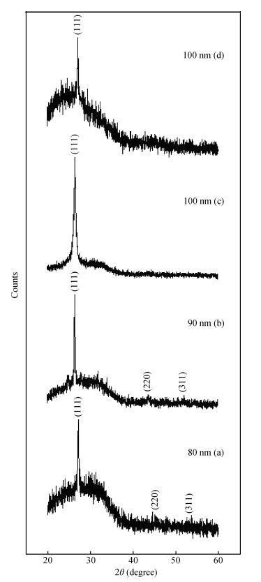
Fig. 1.
XRD spectra of ZnSe/ITO/glass thin films of (a) 80, (b) 90, and (c) 100 nm thickness. (d) The 100 nm thick ZnSe/glass sample is also included for comparison.
SEMICONDUCTOR MATERIALS
A.A. Khurram1, , M. Imran2, Nawazish A. Khan2 and M. Nasir Mehmood3
Corresponding author: A. A. Khurram, Email: khuram_qau@yahoo.com
Abstract: The crystal structure, electrical and optical properties of ZnSe thin films deposited on an In2O3:Sn (ITO) substrate are evaluated for their suitability as the window layer of CdTe thin film solar cells. ZnSe thin films of 80, 90, and 100 nm thickness were deposited by a physical vapor deposition method on Indium tin oxide coated glass substrates. The lattice parameters are increased to 5.834 Å when the film thickness was 100 nm, which is close to that of CdS. The crystallite size is decreased with the increase of film thickness. The optical transmission analysis shows that the energy gap for the sample with the highest thickness has also increased and is very close to 2.7 eV. The photo decay is also studied as a function of ZnSe film thickness.
Keywords: ZnSe thin films, ITO substrate, XRD, optical transmission, photodecay
| [1] | |
| [2] | |
| [3] |
Meysing D M, Reese M O, Warren C W. Evolution of oxygenated cadmium sulfide (CdS:O) during high-temperature CdTe solar cell fabrication. Sol Energy Mater Solar Cells, 2016, 157:276 doi: 10.1016/j.solmat.2016.05.038
|
| [4] |
Han J, Spanheimer C, Haindl G, et al. Optimized chemical bath deposited CdS layers for the improvement of CdTe solar cells. Sol Energy Mater Sol Cells, 2011, 95(3):816 doi: 10.1016/j.solmat.2010.10.027
|
| [5] |
Dang H, Singh V P, Guduru S, et al. Embedded nanowire window layers for enhanced quantum efficiency in window-absorber type solar cells like CdS/CdTe. Sol Energy Mater Sol Cells, 2016, 144:641 doi: 10.1016/j.solmat.2015.09.044
|
| [6] |
Kumara S G, Rao K S R K. Physics and chemistry of CdTe/CdS thin film heterojunction photovoltaic devices:fundamental and critical aspects. Energy Environ Sci, 2014, 7:45 doi: 10.1039/C3EE41981A
|
| [7] |
Poortmans J, Arkhipov V. Thin film solar cells, fabrication characterization and applications. New York: John Willy and Sons, 2006
|
| [8] |
Luque A, Hegedus S. Hand book of photovoltaic science and engineering. UK: John Wiley & Sons, 2003
|
| [9] |
Kasap S, Capper P. Springer handbook of electronic and photonic materials. Canada:Springer, 2006
|
| [10] |
Bacaksiz E, Aksu S, Polat I, et al. The influence of substrate temperature on the morphology, optical and electrical properties of thermal-evaporated ZnSe thin films. J Alloys Compnd, 2009, 487(1):280 http://www.sciencedirect.com/science/article/pii/S0925838809014674
|
| [11] |
Venkatachalam S, Managalaraj S, Narayandass S K. Characterization of vacuum-evaporated ZnSe thin films. Physica B, 2007, 393(1):47 http://www.sciencedirect.com/science/article/pii/S104458030600341X
|
| [12] |
Pankov J I. Optical processes in semiconductors. New York: Dover, 1971
|
| [13] |
Chen L, Zhang D, Zhai G, et al. Comparative study of ZnSe thin films deposited from modified chemical bath solutions with ammonia-containing and ammonia-free precursors. Mater Chem Phys, 2010, 120(2):456 http://www.sciencedirect.com/science/article/pii/S0254058409007214
|
| [14] |
Enriquez J P, Mathew X. Influence of the thickness on structural, optical and electrical properties of chemical bath deposited CdS thin films. Solar Energy Mater Solar Cells, 2003, 76(3):313 doi: 10.1016/S0927-0248(02)00283-0
|
| [15] |
George P J, Sánchez-Juarez A, Nair P K. Doping of chemically deposited intrinsic CdS thin films to n type by thermal diffusion of indium. Appl Phys Lett, 1995, 66:3624 doi: 10.1063/1.113808
|
| [16] |
Joshi N V. Photoconductivity: art, science and technology. New York: Marcel Dekker, 1991
|
| [17] |
Ray B. Ⅱ-Ⅵ compounds. New York:Pergamon Press, 1969
|
| [18] |
Neamen D A. Semiconductor physics and devices. New York: McGraw-Hill, 2007
|
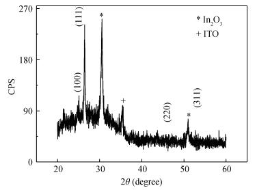
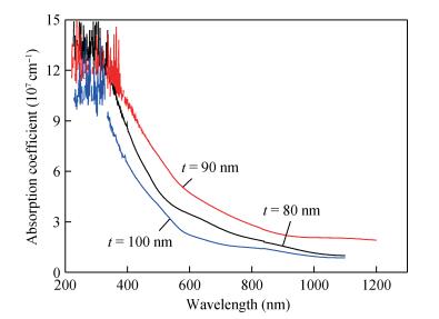
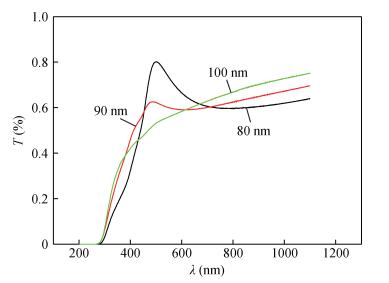
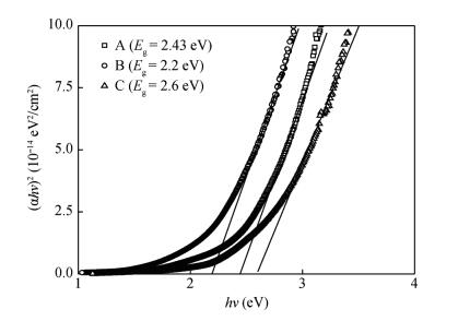
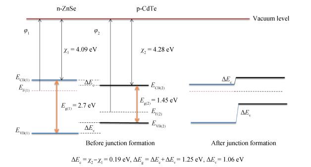
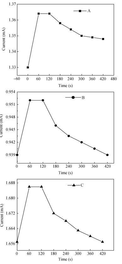
Table 1. The structural parameters of ZnSe thin films calculated from the XRD spectra.

|
 DownLoad: CSV
Table 2. The results of the measurements of electrical conductivity and photosensitivity of ZnSe/ITO/glass thin films.

|
DownLoad: CSV
| [1] | |
| [2] | |
| [3] |
Meysing D M, Reese M O, Warren C W. Evolution of oxygenated cadmium sulfide (CdS:O) during high-temperature CdTe solar cell fabrication. Sol Energy Mater Solar Cells, 2016, 157:276 doi: 10.1016/j.solmat.2016.05.038
|
| [4] |
Han J, Spanheimer C, Haindl G, et al. Optimized chemical bath deposited CdS layers for the improvement of CdTe solar cells. Sol Energy Mater Sol Cells, 2011, 95(3):816 doi: 10.1016/j.solmat.2010.10.027
|
| [5] |
Dang H, Singh V P, Guduru S, et al. Embedded nanowire window layers for enhanced quantum efficiency in window-absorber type solar cells like CdS/CdTe. Sol Energy Mater Sol Cells, 2016, 144:641 doi: 10.1016/j.solmat.2015.09.044
|
| [6] |
Kumara S G, Rao K S R K. Physics and chemistry of CdTe/CdS thin film heterojunction photovoltaic devices:fundamental and critical aspects. Energy Environ Sci, 2014, 7:45 doi: 10.1039/C3EE41981A
|
| [7] |
Poortmans J, Arkhipov V. Thin film solar cells, fabrication characterization and applications. New York: John Willy and Sons, 2006
|
| [8] |
Luque A, Hegedus S. Hand book of photovoltaic science and engineering. UK: John Wiley & Sons, 2003
|
| [9] |
Kasap S, Capper P. Springer handbook of electronic and photonic materials. Canada:Springer, 2006
|
| [10] |
Bacaksiz E, Aksu S, Polat I, et al. The influence of substrate temperature on the morphology, optical and electrical properties of thermal-evaporated ZnSe thin films. J Alloys Compnd, 2009, 487(1):280 http://www.sciencedirect.com/science/article/pii/S0925838809014674
|
| [11] |
Venkatachalam S, Managalaraj S, Narayandass S K. Characterization of vacuum-evaporated ZnSe thin films. Physica B, 2007, 393(1):47 http://www.sciencedirect.com/science/article/pii/S104458030600341X
|
| [12] |
Pankov J I. Optical processes in semiconductors. New York: Dover, 1971
|
| [13] |
Chen L, Zhang D, Zhai G, et al. Comparative study of ZnSe thin films deposited from modified chemical bath solutions with ammonia-containing and ammonia-free precursors. Mater Chem Phys, 2010, 120(2):456 http://www.sciencedirect.com/science/article/pii/S0254058409007214
|
| [14] |
Enriquez J P, Mathew X. Influence of the thickness on structural, optical and electrical properties of chemical bath deposited CdS thin films. Solar Energy Mater Solar Cells, 2003, 76(3):313 doi: 10.1016/S0927-0248(02)00283-0
|
| [15] |
George P J, Sánchez-Juarez A, Nair P K. Doping of chemically deposited intrinsic CdS thin films to n type by thermal diffusion of indium. Appl Phys Lett, 1995, 66:3624 doi: 10.1063/1.113808
|
| [16] |
Joshi N V. Photoconductivity: art, science and technology. New York: Marcel Dekker, 1991
|
| [17] |
Ray B. Ⅱ-Ⅵ compounds. New York:Pergamon Press, 1969
|
| [18] |
Neamen D A. Semiconductor physics and devices. New York: McGraw-Hill, 2007
|


Article views: 5688 Times PDF downloads: 47 Times Cited by: 0 Times
Received: 27 June 2016 Revised: 31 March 2017 Online: Published: 01 September 2017
| Citation: |
A.A. Khurram, M. Imran, Nawazish A. Khan, M. Nasir Mehmood. ZnSe/ITO thin films:candidate for CdTe solar cell window layer[J]. Journal of Semiconductors, 2017, 38(9): 093001. doi: 10.1088/1674-4926/38/9/093001
****
A A Khurram, M Imran, N A Khan, M N Mehmood. ZnSe/ITO thin films:candidate for CdTe solar cell window layer[J]. J. Semicond., 2017, 38(9): 093001. doi: 10.1088/1674-4926/38/9/093001.

|
| [1] | |
| [2] | |
| [3] |
Meysing D M, Reese M O, Warren C W. Evolution of oxygenated cadmium sulfide (CdS:O) during high-temperature CdTe solar cell fabrication. Sol Energy Mater Solar Cells, 2016, 157:276 doi: 10.1016/j.solmat.2016.05.038
|
| [4] |
Han J, Spanheimer C, Haindl G, et al. Optimized chemical bath deposited CdS layers for the improvement of CdTe solar cells. Sol Energy Mater Sol Cells, 2011, 95(3):816 doi: 10.1016/j.solmat.2010.10.027
|
| [5] |
Dang H, Singh V P, Guduru S, et al. Embedded nanowire window layers for enhanced quantum efficiency in window-absorber type solar cells like CdS/CdTe. Sol Energy Mater Sol Cells, 2016, 144:641 doi: 10.1016/j.solmat.2015.09.044
|
| [6] |
Kumara S G, Rao K S R K. Physics and chemistry of CdTe/CdS thin film heterojunction photovoltaic devices:fundamental and critical aspects. Energy Environ Sci, 2014, 7:45 doi: 10.1039/C3EE41981A
|
| [7] |
Poortmans J, Arkhipov V. Thin film solar cells, fabrication characterization and applications. New York: John Willy and Sons, 2006
|
| [8] |
Luque A, Hegedus S. Hand book of photovoltaic science and engineering. UK: John Wiley & Sons, 2003
|
| [9] |
Kasap S, Capper P. Springer handbook of electronic and photonic materials. Canada:Springer, 2006
|
| [10] |
Bacaksiz E, Aksu S, Polat I, et al. The influence of substrate temperature on the morphology, optical and electrical properties of thermal-evaporated ZnSe thin films. J Alloys Compnd, 2009, 487(1):280 http://www.sciencedirect.com/science/article/pii/S0925838809014674
|
| [11] |
Venkatachalam S, Managalaraj S, Narayandass S K. Characterization of vacuum-evaporated ZnSe thin films. Physica B, 2007, 393(1):47 http://www.sciencedirect.com/science/article/pii/S104458030600341X
|
| [12] |
Pankov J I. Optical processes in semiconductors. New York: Dover, 1971
|
| [13] |
Chen L, Zhang D, Zhai G, et al. Comparative study of ZnSe thin films deposited from modified chemical bath solutions with ammonia-containing and ammonia-free precursors. Mater Chem Phys, 2010, 120(2):456 http://www.sciencedirect.com/science/article/pii/S0254058409007214
|
| [14] |
Enriquez J P, Mathew X. Influence of the thickness on structural, optical and electrical properties of chemical bath deposited CdS thin films. Solar Energy Mater Solar Cells, 2003, 76(3):313 doi: 10.1016/S0927-0248(02)00283-0
|
| [15] |
George P J, Sánchez-Juarez A, Nair P K. Doping of chemically deposited intrinsic CdS thin films to n type by thermal diffusion of indium. Appl Phys Lett, 1995, 66:3624 doi: 10.1063/1.113808
|
| [16] |
Joshi N V. Photoconductivity: art, science and technology. New York: Marcel Dekker, 1991
|
| [17] |
Ray B. Ⅱ-Ⅵ compounds. New York:Pergamon Press, 1969
|
| [18] |
Neamen D A. Semiconductor physics and devices. New York: McGraw-Hill, 2007
|

 WeChat ID
Journal of Semiconductors © 2017 All Rights Reserved 京ICP备05085259号-2


