Fig. 1.
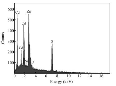
Elemental composition analysis of Cd1-xZnxS nanoparticles.
SEMICONDUCTOR MATERIALS
Abideen A. Ibiyemi1, , Ayodeji O Awodugba2, Olusola Akinrinola2 and Abass A Faremi1
Corresponding author: Abideen A. Ibiyemi, Email: abideen.ibiyemi@fuoye.edu.ng
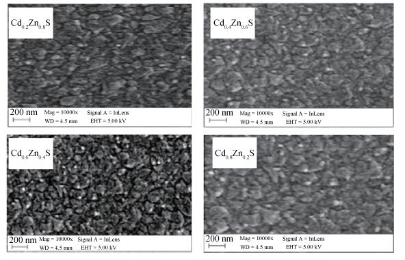
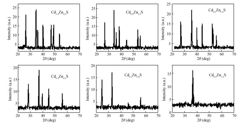
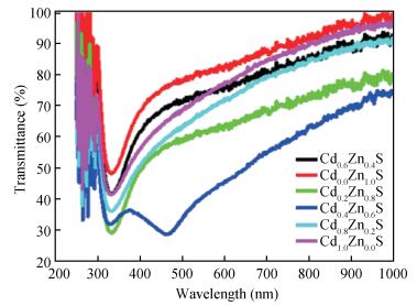
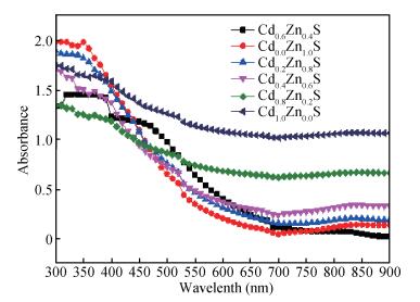
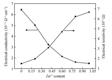
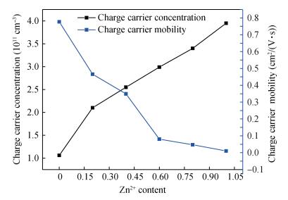
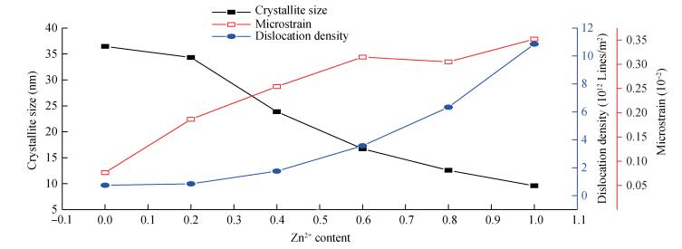
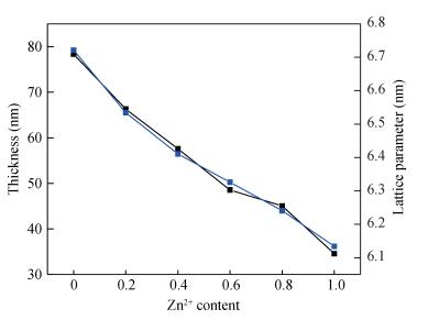
Abstract: Cd1-xZnxS nanoparticles were grown on pre-cleaned glass substrates using microwave-assisted chemical bath deposition technique. Nanoparticles obtained by this method were smooth, uniform, good adherent, brownish yellow in color where the brightness of the yellow color nature decreases with increasing Zn2+ content. The elemental composition analysis confirmed that the nanoparticles comprise of Cd2+, Zn2+and S2-. Scanning electron microscope images confirmed the surface uniformity of the Cd1-xZnxS nanoparticles devoid of any void, pinhole or cracks and covered the substrate well. The particle size also decreases with increasing Zn ion content. X-ray diffraction (XRD) indicates the hexagonal structure (002) without phase transition. The grain size decreases from 36.45 to 9.60 nm, dislocation density increases from 0.000745 to 0.01085 Line2/m2 and lattice parameter decreased from 6.868 to 6.155 nm with increasing Zn2+ content. The best transmittance of about 95% was achieved for x=1.0. The nanoparticles showed reduction in the absorbance as Zn ion content increased. Four point probe revealed that the electrical resistivity increased from 1.51×10¹⁰ to 6.67×10¹⁰ Ω ·cm while electrical conductivity decreases from 6.62×10⁻¹¹ to 1.49×10⁻¹¹ (Ω ·cm)-1 with increasing Zn2+ content. The other electrical properties such as sheet resistance increased from 1.52×10⁸ to 1.58×10⁸Ω, charge carrier mobility decreased from 0.777 to 0.0105 cm2/(V·s) and charge carrier density increased from 1.06×10¹² to 3.95×1012 cm-3.
Keywords: Cd1-xZnxS, nanoparticles, transmittance, XRD, SEM, carrier mobility
| [1] |
Awodugba A O, Adedokun O. On the physical and optical characteristics of CdS thin films deposited by chemical bath deposition technique. Pac J Sci Technol, 2011, 12(2):334
|
| [2] |
Celalettin B M, Orhan N. Band alignment of Cd1-xZnxS produced by spray pyrolysis method. Thin Solid Films, 2010, 518:1925 doi: 10.1016/j.tsf.2009.07.142
|
| [3] |
Oztas M, Bedir M. Some properties of Cd1-xZnxS and Cd1-xZnxS(In) thin films prepared by pyrolytic spray technique. J Appl Sci, 2005, 4:534
|
| [4] |
Dona J M, Herrero J. Chemical bath codeposited CdS-ZnS characterization. Thin Solid Films, 2002, 268:5
|
| [5] |
Illican S, Caglar Y, Caglar M. Effect of the substrate temperatures on the optical properties of the Cd0.22Zn0.78S thin films by spray pyrolysis method. Physica Macedonica, 2006, 56:43
|
| [6] |
Dzhafarov T D, Ongul F, Karabay I. Formation of CdZnS thin films by Zn diffusion. J Appl Phys, 2006, 39:32
|
| [7] |
Ravangave L S, Biradar U V. Study of structural, morphological and electrical properties of CdxZn1-xS thin films. IOSR J Appl Phys, 2013, 3(3):41 doi: 10.9790/4861
|
| [8] |
Kumar T P, Sankaranarayanan K. Growth and characterization of CdZnS thin films by short duration microwave assisted chemical bath deposition technique. Chalcogenide Lett, 2009, 6(10):555
|
| [9] |
Vidhya Y, Velumani A. Electrical characterization of chemically deposited thin films under magnetic field. Phys Stat Sol, 2009, 167:143
|
| [10] |
Patidar D, Saxena N S, Sharma K, et al. Conduction mechanism in CdZnS thin films. Optoelectron Adv Mater Rapid Commun, 2007, 1(7):329
|
| [11] |
Mustapha G, Chowdhury M R I, Saha D K, et al. Annealing effects on the properties of chemically deposited CdS thin films at ambient condition. Dhaka Univ J Sci, 2012, 60(2):283 http://www.banglajol.info/index.php/DUJS/article/view/11536
|
| [12] |
Al-Tememee N A, Saeed N M, Al-Dujayli S M A, et al. The effect of Zn concentration on the optical properties of Cd1-xZnxS films for solar cells applications. Adv Mater Phys Chem, 2012, 2:69 doi: 10.4236/ampc.2012.22012
|
| [13] |
Gorji N E. Deposition and doping of CdS/CdTe thin film solar cells. J Semicond, 2015, 36(5):054001 doi: 10.1088/1674-4926/36/5/054001
|
| [14] |
Errai M, El Kaaouachi A, El Idrissi H. Variable range hopping conduction in n-CdSe samples at very low temperature. J Semicond, 2015, 36(12):122001 doi: 10.1088/1674-4926/36/12/122001
|
| [15] |
Das S, Mukhopadhyay A K, Datta S, et al. Prospects of microwave processing:an overview. Bull Mater Sci, 2009, 32(1):1 doi: 10.1007/s12034-009-0001-4
|


Article views: 5141 Times PDF downloads: 25 Times Cited by: 0 Times
Received: 08 August 2016 Revised: 18 March 2017 Online: Published: 01 September 2017
| Citation: |
Abideen A. Ibiyemi, Ayodeji O Awodugba, Olusola Akinrinola, Abass A Faremi. Zinc-doped CdS nanoparticles synthesized by microwave-assisted deposition[J]. Journal of Semiconductors, 2017, 38(9): 093002. doi: 10.1088/1674-4926/38/9/093002
****
A A Ibiyemi, A O Awodugba, O Akinrinola, A A Faremi. Zinc-doped CdS nanoparticles synthesized by microwave-assisted deposition[J]. J. Semicond., 2017, 38(9): 093002. doi: 10.1088/1674-4926/38/9/093002.

|
| [1] |
Awodugba A O, Adedokun O. On the physical and optical characteristics of CdS thin films deposited by chemical bath deposition technique. Pac J Sci Technol, 2011, 12(2):334
|
| [2] |
Celalettin B M, Orhan N. Band alignment of Cd1-xZnxS produced by spray pyrolysis method. Thin Solid Films, 2010, 518:1925 doi: 10.1016/j.tsf.2009.07.142
|
| [3] |
Oztas M, Bedir M. Some properties of Cd1-xZnxS and Cd1-xZnxS(In) thin films prepared by pyrolytic spray technique. J Appl Sci, 2005, 4:534
|
| [4] |
Dona J M, Herrero J. Chemical bath codeposited CdS-ZnS characterization. Thin Solid Films, 2002, 268:5
|
| [5] |
Illican S, Caglar Y, Caglar M. Effect of the substrate temperatures on the optical properties of the Cd0.22Zn0.78S thin films by spray pyrolysis method. Physica Macedonica, 2006, 56:43
|
| [6] |
Dzhafarov T D, Ongul F, Karabay I. Formation of CdZnS thin films by Zn diffusion. J Appl Phys, 2006, 39:32
|
| [7] |
Ravangave L S, Biradar U V. Study of structural, morphological and electrical properties of CdxZn1-xS thin films. IOSR J Appl Phys, 2013, 3(3):41 doi: 10.9790/4861
|
| [8] |
Kumar T P, Sankaranarayanan K. Growth and characterization of CdZnS thin films by short duration microwave assisted chemical bath deposition technique. Chalcogenide Lett, 2009, 6(10):555
|
| [9] |
Vidhya Y, Velumani A. Electrical characterization of chemically deposited thin films under magnetic field. Phys Stat Sol, 2009, 167:143
|
| [10] |
Patidar D, Saxena N S, Sharma K, et al. Conduction mechanism in CdZnS thin films. Optoelectron Adv Mater Rapid Commun, 2007, 1(7):329
|
| [11] |
Mustapha G, Chowdhury M R I, Saha D K, et al. Annealing effects on the properties of chemically deposited CdS thin films at ambient condition. Dhaka Univ J Sci, 2012, 60(2):283 http://www.banglajol.info/index.php/DUJS/article/view/11536
|
| [12] |
Al-Tememee N A, Saeed N M, Al-Dujayli S M A, et al. The effect of Zn concentration on the optical properties of Cd1-xZnxS films for solar cells applications. Adv Mater Phys Chem, 2012, 2:69 doi: 10.4236/ampc.2012.22012
|
| [13] |
Gorji N E. Deposition and doping of CdS/CdTe thin film solar cells. J Semicond, 2015, 36(5):054001 doi: 10.1088/1674-4926/36/5/054001
|
| [14] |
Errai M, El Kaaouachi A, El Idrissi H. Variable range hopping conduction in n-CdSe samples at very low temperature. J Semicond, 2015, 36(12):122001 doi: 10.1088/1674-4926/36/12/122001
|
| [15] |
Das S, Mukhopadhyay A K, Datta S, et al. Prospects of microwave processing:an overview. Bull Mater Sci, 2009, 32(1):1 doi: 10.1007/s12034-009-0001-4
|

 WeChat ID
Journal of Semiconductors © 2017 All Rights Reserved 京ICP备05085259号-2

 DownLoad: