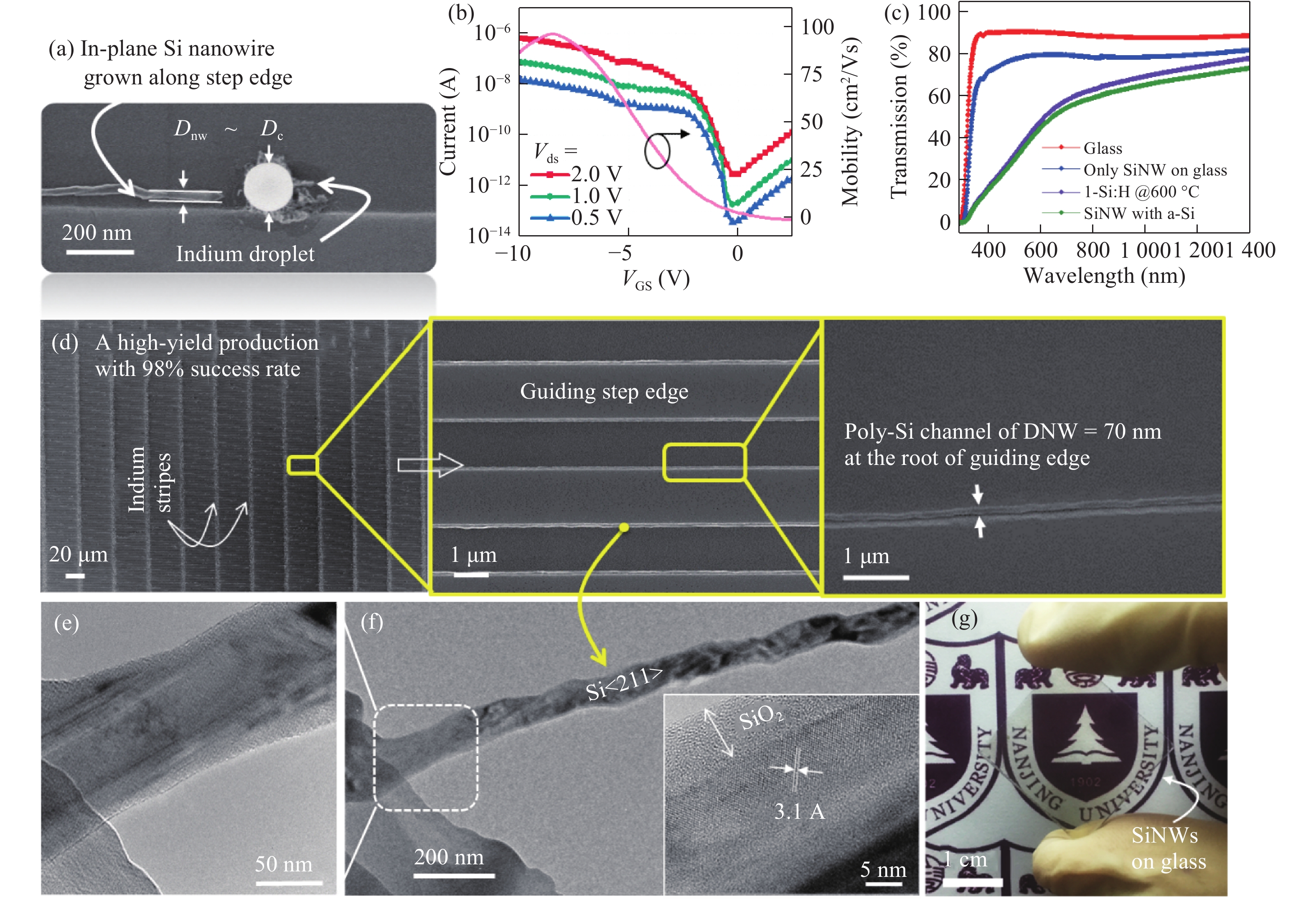
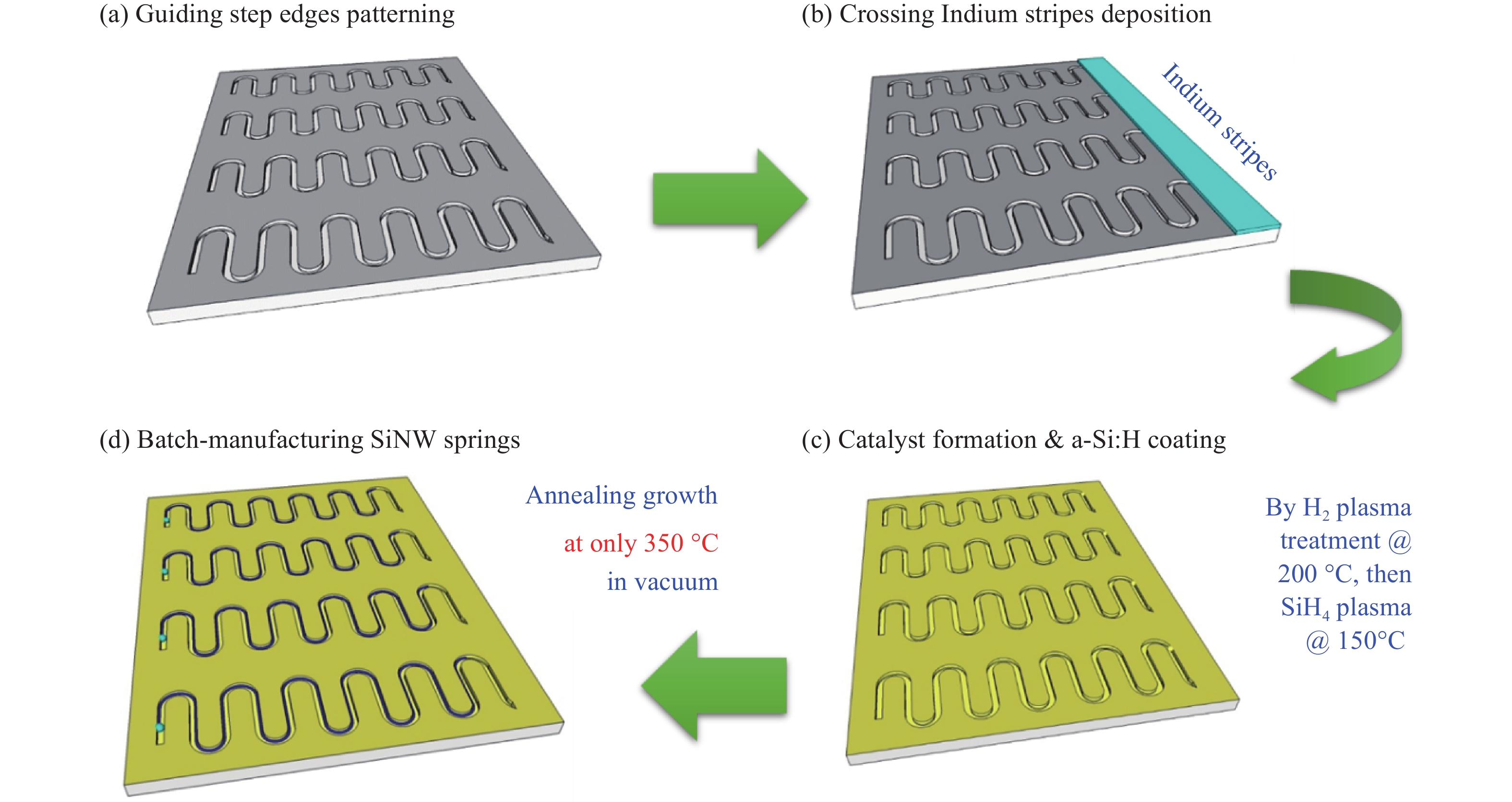
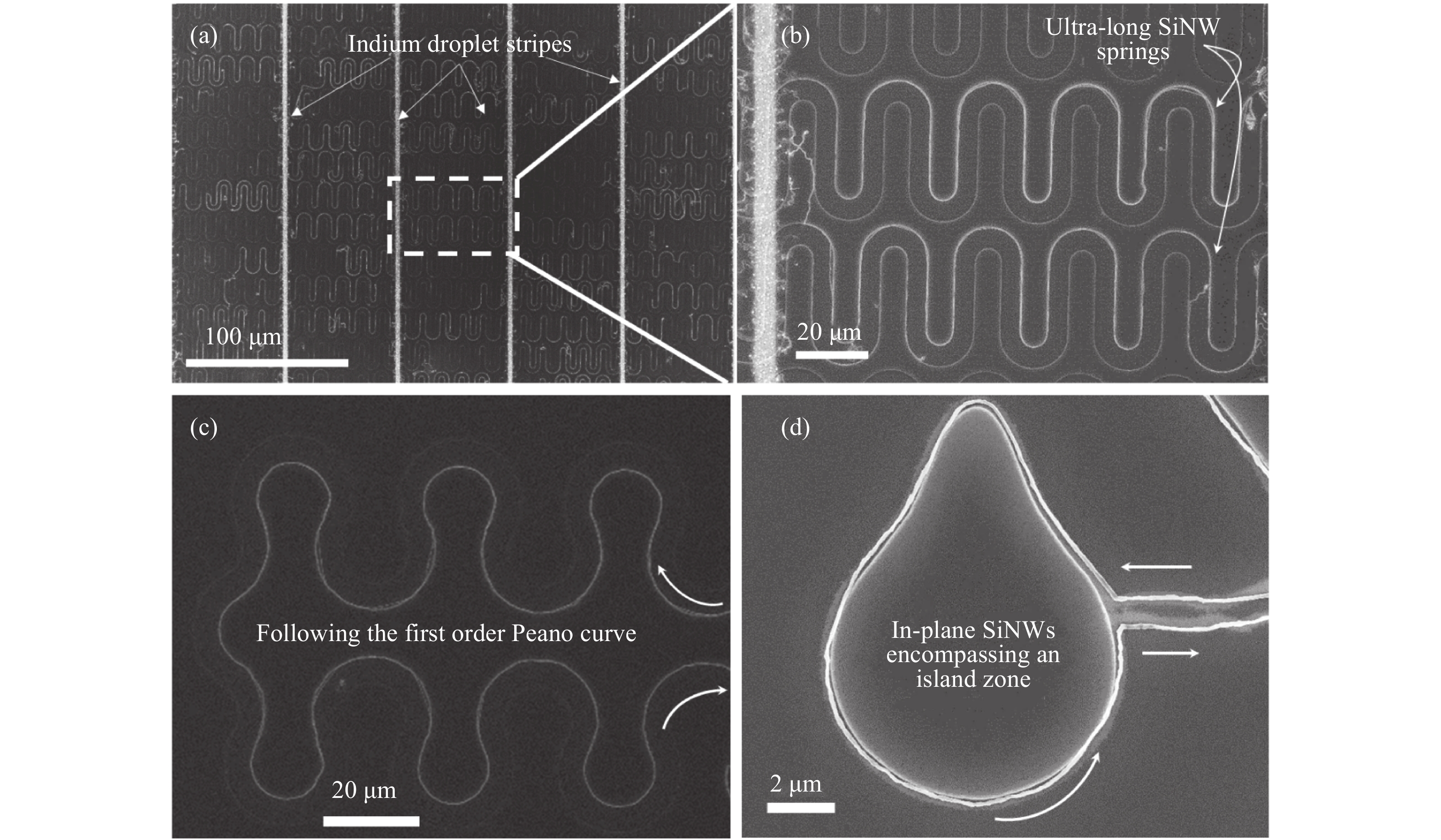
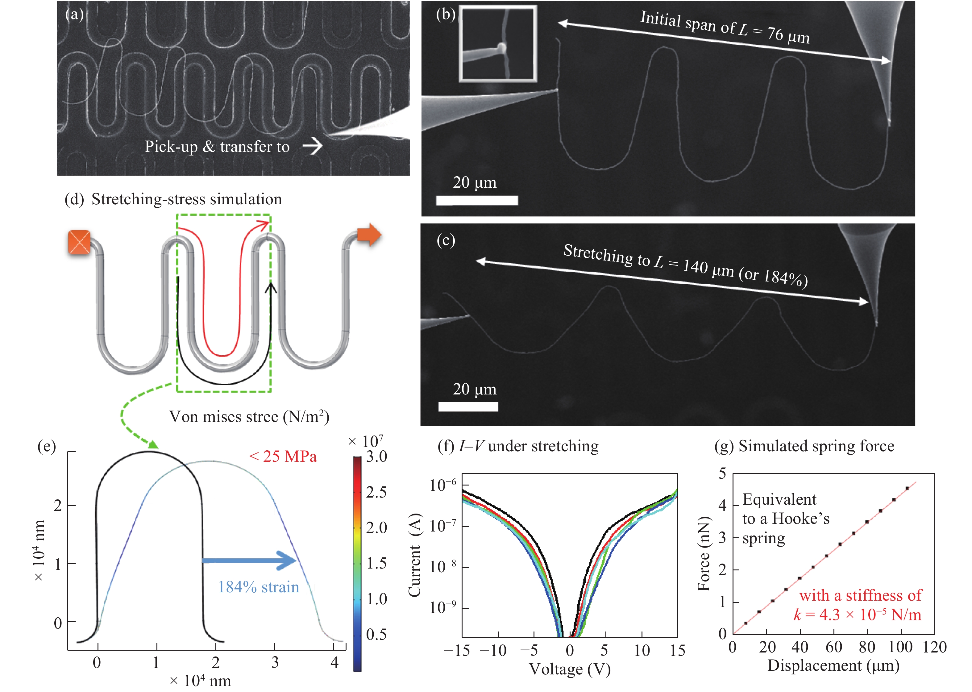
| [1] |
Kim J, Salvatore G A, Araki H, et al. Stretchable optoelectronic systems for wireless optical characterization of the skin. Sci Adv, 2016, 2: e1600418 doi: 10.1126/sciadv.1600418 |
| [2] |
Xu B, Rogers J A. Mechanics-driven approaches to manufacturing—A perspective. Extrem Mech Lett, 2016, 7: 44 doi: 10.1016/j.eml.2015.12.012 |
| [3] |
|
| [4] |
Hussain A M, Hussain M M. CMOS-technology-enabled flexible and stretchable electronics for internet of everything applications. Adv Mater, 2016, 28: 4219 doi: 10.1002/adma.v28.22 |
| [5] |
Hammock M L, Chortos A, Tee B C K, et al. The evolution of electronic skin (e-skin): a brief history, design considerations, and recent progress. Adv Mater, 2013, 25: 5997 doi: 10.1002/adma.201302240 |
| [6] |
Cheng T, Zhang Y, Lai. Stretchable thin-film electrodes for flexible electronics with high deformability and stretchability. Adv Mater, 2015, 27: 3349 doi: 10.1002/adma.v27.22 |
| [7] |
Wang Y, Zhu C, Pfattner R, et al. A highly stretchable, transparent, and conductive polymer. Sci Adv, 2017, 3: e1602076 doi: 10.1126/sciadv.1602076 |
| [8] |
Roberts M E, Mannsfeld S C B, Stoltenberg R M, et al. Flexible, plastic transistor-based chemical sensors. Org Electron, 2009, 10: 377 doi: 10.1016/j.orgel.2008.12.001 |
| [9] |
|
| [10] |
Arias A C, MacKenzie J D, McCulloch I, et al. Materials and applications for large area electronics: solution-based approaches. Chem Rev, 2010, 110: 3 doi: 10.1021/cr900150b |
| [11] |
Lei Z, Wang Q, Sun S, et al. A bioinspired mineral hydrogel as a self-healable, mechanically adaptable ionic skin for highly sensitive pressure sensing. Adv Mater, 2017, 29: 1700321 doi: 10.1002/adma.201700321 |
| [12] |
Lin P, Yan F. Organic thin-film transistors for chemical and biological sensing. Adv Mater, 2012, 24: 34 doi: 10.1002/adma.201103334 |
| [13] |
Wang L, Liu P, Guan P, et al. In situ atomic-scale observation of continuous and reversible lattice deformation beyond the elastic limit. Nat Commun, 2013, 4: 2413 doi: 10.1038/ncomms3413 |
| [14] |
Wang L, Zheng K, Zhang Z, et al. Direct atomic-scale imaging about the mechanisms of ultralarge bent straining in Si nanowires. Nano Lett, 2011, 11: 2382 doi: 10.1021/nl200735p |
| [15] |
Zheng K, Han X, Wang L, et al. Atomic mechanisms governing the elastic limit and the incipient plasticity of bending Si nanowires. Nano Lett, 2009, 9: 2471 doi: 10.1021/nl9012425 |
| [16] |
Zhu Y, Xu F, Qin Q, et al. Mechanical properties of vapor-liquid-solid synthesized silicon nanowires. Nano Lett, 2009, 9: 3934 doi: 10.1021/nl902132w |
| [17] |
Khang D Y, Jiang H, Huang Y, et al. A stretchable form of single-crystal silicon for high-performance electronics on rubber substrates. Science, 2006, 311: 208 doi: 10.1126/science.1121401 |
| [18] |
Kim H W, Shim S H. Helical nanostructures of SiO x synthesized through the heating of Co-coated substrates. Appl Surf Sci, 2007, 253: 3664 doi: 10.1016/j.apsusc.2006.07.083 |
| [19] |
Zhang H F, Wang C M, Buck E C, et al. Synthesis, characterization, and manipulation of helical SiO 2 nanosprings. Nano Lett, 2003, 3: 577 doi: 10.1021/nl0341180 |
| [20] |
Swain B S, Lee S S, Lee S H, et al. Transformation of silicon nanowires to nanocoils by annealing in reducing atmosphere. J Cryst Growth, 2011, 327: 276 doi: 10.1016/j.jcrysgro.2011.06.018 |
| [21] |
Tang Y H, Zhang Y F, Wang N, et al. Morphology of Si nanowires synthesized by high-temperature laser ablation. J Appl Phys, 1999, 85: 7981 doi: 10.1063/1.369389 |
| [22] |
Tian B, Xie P, Kempa T J, et al. Single-crystalline kinked semiconductor nanowire superstructures. Nat Nano, 2009, 4: 824 doi: 10.1038/nnano.2009.304 |
| [23] |
Lugstein A, Steinmair M, Hyun Y J, et al. Pressure-induced orientation control of the growth of epitaxial silicon nanowires. Nano Lett, 2008, 8: 2310 doi: 10.1021/nl8011006 |
| [24] |
Musin I R, Filler M A. Chemical control of semiconductor nanowire kinking and superstructure. Nano Lett, 2012, 12: 3363 doi: 10.1021/nl204065p |
| [25] |
Schmidt V, Wittemann J V, Senz S, et al. Silicon nanowires: a review on aspects of their growth and their electrical properties. Adv Mater, 2009, 21: 2681 doi: 10.1002/adma.200803754 |
| [26] |
Wagner R S, Ellis W C. Vapor-liquid-solid mechanism of single crystal growth. Appl Phys Lett, 1964, 4: 89 doi: 10.1063/1.1753975 |
| [27] |
Xu F, Lu W, Zhu Y. Controlled 3D buckling of silicon nanowires for stretchable electronics. ACS Nano, 2011, 5: 672 doi: 10.1021/nn103189z |
| [28] |
Kim D H, Ahn J H, Choi W M, et al. Stretchable and foldable silicon integrated circuits. Science, 2008, 320: 507 doi: 10.1126/science.1154367 |
| [29] |
Jang K I, Li K, Chung H U, et al. Self-assembled three dimensional network designs for soft electronics. Nat Commun, 2017, 8: 15894
|
| [30] |
Sepulveda A C C, Cordero M S D, Carreño A A A, et al. Stretchable and foldable silicon-based electronics. Appl Phys Lett, 2017, 110: 134103 doi: 10.1063/1.4979545 |
| [31] |
Rojas J P, Arevalo A, Foulds I G, et al. Design and characterization of ultra-stretchable monolithic silicon fabric. Appl Phys Lett, 2014, 105: 154101 doi: 10.1063/1.4898128 |
| [32] |
Kim J, Lee M, Shim H J, et al. Stretchable silicon nanoribbon electronics for skin prosthesis. Nat Commun, 2014, 5: 5747 doi: 10.1038/ncomms6747 |
| [33] |
Pevzner A, Engel Y, Elnathan R, et al. Confinement-guided shaping of semiconductor nanowires and nanoribbons: " writing with nanowires”. Nano Lett, 2012, 12: 7 doi: 10.1021/nl201527h |
| [34] |
Gonzalez M, Axisa F, Bulcke M V, et al. Design of metal interconnects for stretchable electronic circuits. Microelectron Rel, 2008, 48: 825 doi: 10.1016/j.microrel.2008.03.025 |
| [35] |
Vanfleteren J, Gonzalez M, Bossuyt F, et al. Printed circuit board technology inspired stretchable circuits. MRS Bull, 2012, 37: 254 doi: 10.1557/mrs.2012.48 |
| [36] |
Yu L, Alet P J, Picardi G, et al. An in-plane solid-liquid-solid growth mode for self-avoiding lateral silicon nanowires. Phys Rev Lett, 2009, 102: 125501 doi: 10.1103/PhysRevLett.102.125501 |
| [37] |
Yu L, P Roca i Cabarrocas. Initial nucleation and growth of in-plane solid-liquid-solid silicon nanowires catalyzed by indium. Phys Rev B, 2009, 80: 085313 doi: 10.1103/PhysRevB.80.085313 |
| [38] |
Yu L, P Roca i Cabarrocas. Growth mechanism and dynamics of in-plane solid-liquid-solid silicon nanowires. Phys Rev B, 2010, 81: 085323 doi: 10.1103/PhysRevB.81.085323 |
| [39] |
Scarontich I, Car R, Parrinello M. Amorphous silicon studied by ab initio molecular dynamics: preparation, structure, and properties. Phys Rev B, 1991, 44: 11092 doi: 10.1103/PhysRevB.44.11092 |
| [40] |
Roorda S, Doorn S, Sinke W C, et al. Calorimetric evidence for structural relaxation in amorphous silicon. Phys Rev Lett, 1989, 62: 1880 doi: 10.1103/PhysRevLett.62.1880 |
| [41] |
Yu L P. Morphology control and growth dynamics of in-plane solid–liquid–solid silicon nanowires. Physica E, 2012, 44: 1045 doi: 10.1016/j.physe.2011.06.005 |
| [42] |
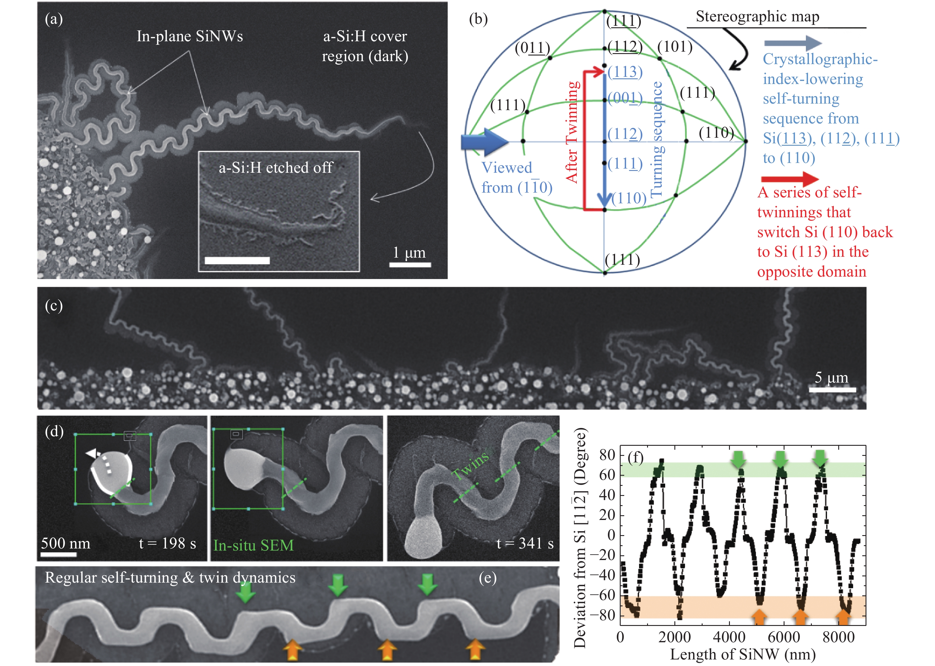
Xue Z, Xu M, Li X, et al. In-plane self-turning and twin dynamics renders large stretchability to mono-like zigzag silicon nanowire springs. Adv Func Mater, 2016, 26: 5352 doi: 10.1002/adfm.201600780 |
| [43] |
Xue Z, Xu M, Zhao Y, et al. Engineering island-chain silicon nanowires via a droplet mediated Plateau-Rayleigh transformation. Nat Commun, 2016, 7: 12836 doi: 10.1038/ncomms12836 |
| [44] |
Shin N, Chi M, Howe J Y, et al. Rational defect introduction in silicon nanowires. Nano Lett, 2013, 13: 1928 doi: 10.1021/nl3042728 |
| [45] |
Algra R E, Verheijen M A, Borgstrom M T, et al. Twinning superlattices in indium phosphide nanowires. Nature, 2008, 456: 369 doi: 10.1038/nature07570 |
| [46] |
Li X, Wei X, Xu T, et al. Remarkable and crystal-structure-dependent piezoelectric and piezoresistive effects of InAs nanowires. Adv Mater, 2015, 27: 2852 doi: 10.1002/adma.v27.18 |
| [47] |
Li X, Wei X L, Xu T T, et al. Mechanical properties of individual InAs nanowires studied by tensile tests. Appl Phys Lett, 2014, 104: 103110 doi: 10.1063/1.4868133 |
| [48] |
Xu M, Xue Z, Yu L, et al. Operating principles of in-plane silicon nanowires at simple step-edges. Nanoscale, 2015, 7: 5197 doi: 10.1039/C4NR06531J |
| [49] |
Yu L, Moustapha O, Oudwan M, et al. Guided growth of in-plane lateral SiNWs led by indium catalysts. Mater Res Soc Symp Proc, 2009, 1178E: AA07
|
| [50] |
Yu L, Oudwan M, Moustapha O, et al. Guided growth of in-plane silicon nanowires. Appl Phys Lett, 2009, 95: 113106 doi: 10.1063/1.3227667 |
| [51] |
Yu L, Chen W, O'Donnell B, et al. Growth-in-place deployment of in-plane silicon nanowires. Appl Phys Lett, 2011, 99: 203104 doi: 10.1063/1.3659895 |
| [52] |
Xu M, Wang J, Xue Z, et al. High performance transparent in-plane silicon nanowire Fin-TFTs via a robust nano-droplet-scanning crystallization dynamics. Nanoscale, 2017, 9: 10350 doi: 10.1039/C7NR02825C |
| [53] |
Chen W, Yu L, Misra S, et al. Incorporation and redistribution of impurities into silicon nanowires during metal-particle-assisted growth. Nat Commun, 2014, 5: 4134
|
| [54] |
Xue Z, Sun M, Zhao Y, et al. Deterministic line-shape programming of silicon nanowires for extremely stretchable springs and electronics. Nano Lett, 2017, 17: 7638
|
| [55] |
O'Mara W, Herring R B, Hunt L P. Handbook of semiconductor silicon technology. Crest Publishing House, 2007
|


 DownLoad: