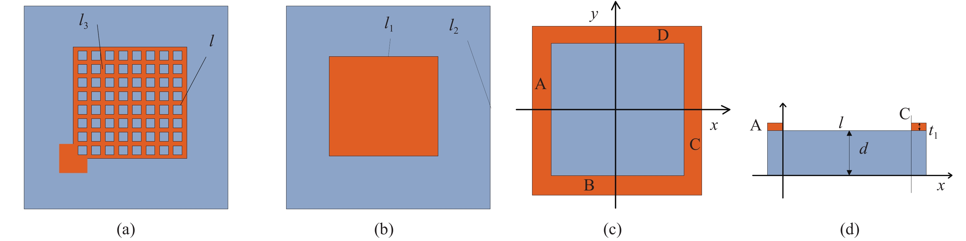
Processing math: 100%
J. Semicond. > 2018, Volume 39 > Issue 11 > 114008

SEMICONDUCTOR DEVICES

Memory characteristics of microcavity dielectric barrier discharge

Yanzhou Sun, Xiaoqian Liu, Dati Su and Huibin Yang

+ Author Affiliations

 Corresponding author: Xiaoqian Liu, Email: 13253567216@163.com

DOI: 10.1088/1674-4926/39/11/114008

PDF

Turn off MathJax

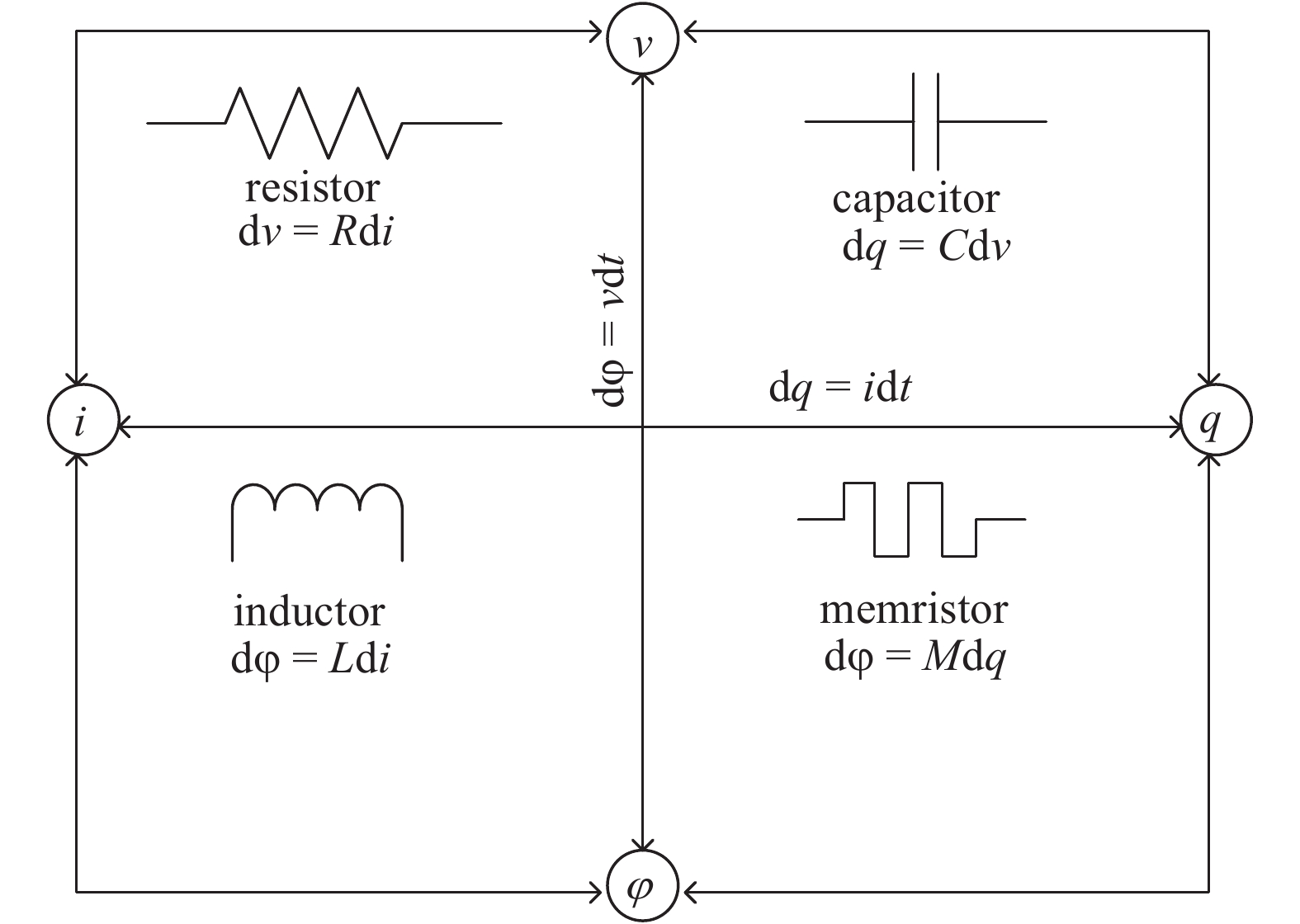
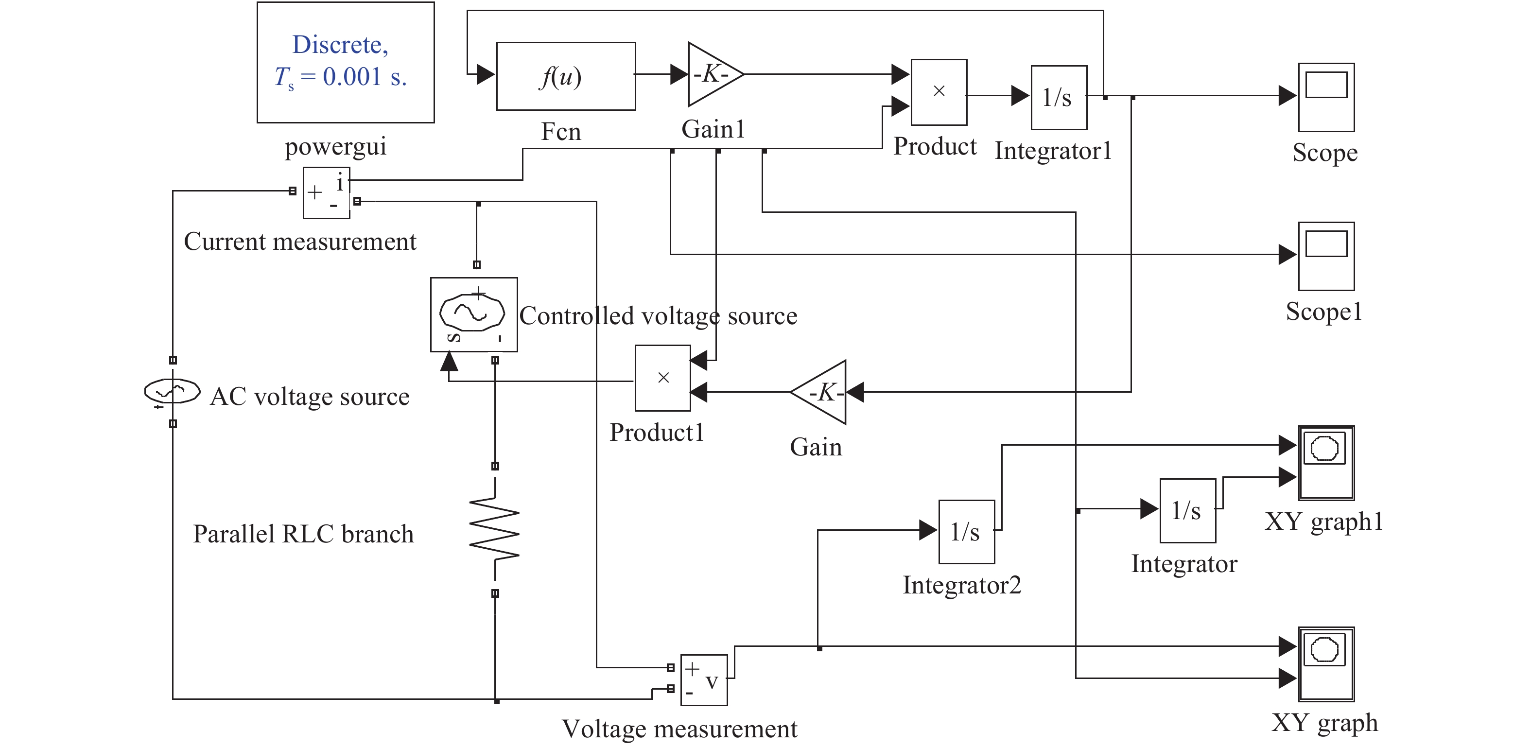
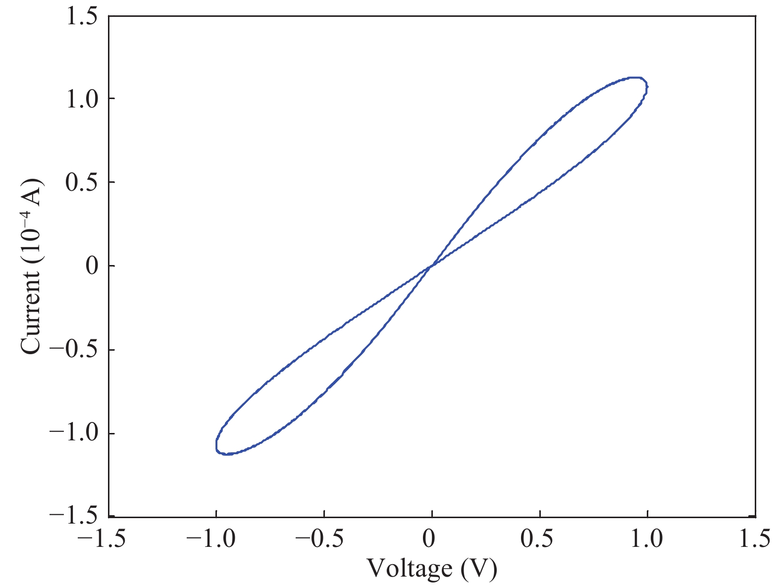
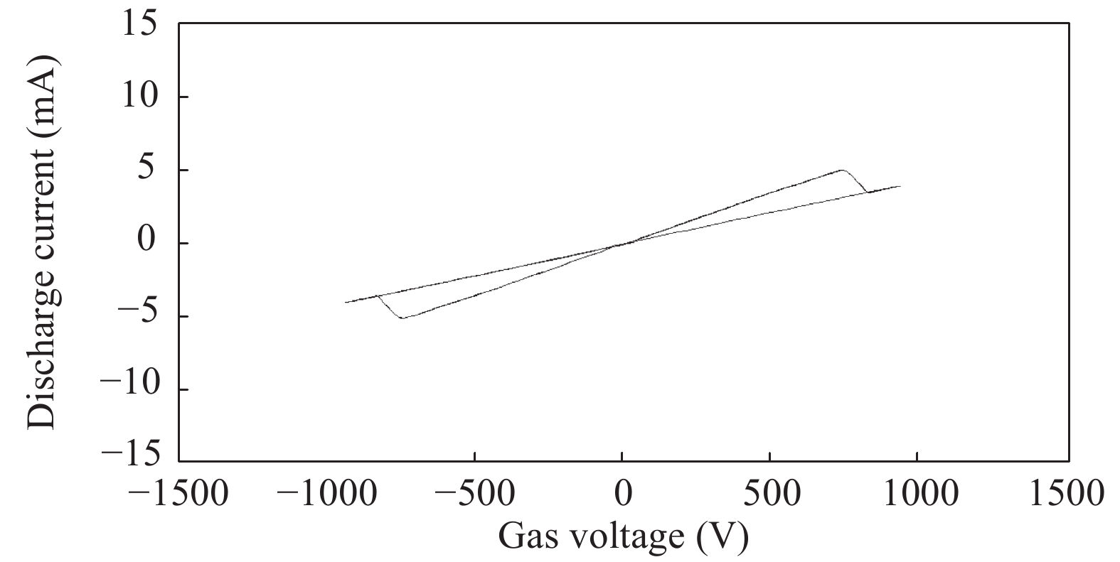
Abstract: The nonlinear resistance characteristics of microcavity dielectric barrier discharge are mainly studied in the paper. A simulation model of microcavity dielectric barrier discharge is herein built to study the relationship between voltage and current in the process of discharge, and thus its I–V characteristic curve can be obtained. The I–V characteristics of the memristor are analyzed and compared with the I–V characteristics of the dielectric barrier discharge; it can be found that the I–V characteristics of the microcavity dielectric barrier discharge are similar to the characteristics of the memristor by analyzing them. The memory characteristics of microcavity dielectric barrier discharge are further analyzed.

Key words: microcavity dielectric barrier dischargememristorI–V characteristicmemory characteristics

The full name of a memristor is memory resistor: its concept was first proposed by Cai, an ethnic Chinese scientist at the University of California, Berkeley, in 1971[1]. He was studying the relationship between current i, voltage v, charge q and magnetic flux φ; he inferred that there should be a fourth basic circuit component according to the circuit of the completeness and symmetry theory besides resistors, capacitors and inductors, which are the three basic circuit elements. Further, he represented the relationship between charge and magnetic flux. This element is the memristor.

Then he introduced the nonlinear dynamic system—the memristive system[2]. In 2003, Professor Cai introduced the nonlinear circuit of a memristor based on nano devices[3]. However, the memristor did not draw much attention until the first memristor was first manufactured by the Hewlett Packard Laboratory in May 2008. In addition, this achievement was published in Nature and proved Chua’s theory was right. Since then, it has become a familiar idea with physicists. The studies of memristors are mainly concentrated on fabrication of the memristors, non-linear circuits, and software simulation[4]. In the 1990s, Prof. Yang claimed that I–V characteristics of gas discharge lamps were similar to the characteristics of flow control memristors[5]. Moreover, some research mainly focused on the modeling[6, 7], while other research concentrated on its applications[8, 9].

A Dielectric Barrier Discharge is the electrical discharge under high pressure between two electrodes separated by an insulating dielectric barrier; this insulating dielectric barrier could be laid on the electrode or the discharge space[10]. This structure works when alternating voltage is added on the electrodes. There is no noise generated in the discharge process, dielectric barrier discharge is therefore also known as silent discharge. Microcavity structure is a special type of discharge structure, where the dielectric barrier discharge can attribute into two categories according to the discharge structure, namely, volume discharge and surface discharge. The volume discharge will discharge running through the whole gas gap between two electrodes. The dielectric barrier discharge of plate electrodes or coaxial tube electrodes belongs to this type. The surface discharge means that it will bring an asymmetrical distribution of electric field near the electrodes when there are some linear small curvature radius electrodes around the insulating medium. Meanwhile, corona and discharge along the dielectric surface will appear on the surface of the dielectric near the electrodes.

From the previous researches on microcavity dielectric barrier discharge, it can be found that the gas voltage and discharge current have the character of a memristor in the discharge process. In this paper, the charge accumulation of the dielectric barrier discharge and the charge variation of the memristor from the perspective of the discharge mechanism of the microcavity dielectric barrier discharge and the resistance variation characteristic of the memristor are analyzed, and a detailed comparison of the I–V characteristics between the microcavity dielectric barrier discharge and the memristor is presented. However, there are still some technical problems in the manufacture of memristors at present.

Microelectrode structure is composed of a high voltage electrode, the microcavity, the dielectric layer and the grounding electrode. The two sides of the dielectric pane are used as the high voltage electrode and the grounding electrode respectively. The polyimide is selected as the dielectric plate. The high voltage electrode and the ground electrode are symmetrically located in the center of the dielectric plate. The structure of the high voltage electrode, the ground electrode, the single microcavity and the relative electrode section are shown in Fig. 1.

Figure  1.  (Color online) Microcavity structure of electrode: (a) high voltage electrode, (b) ground electrode, (c) single microcavity and (d) electrode section of A, C.

Each edge of the two electrodes has an electrical safety distance. The discharge electrode is in the form of an array, where microcavities with different volumes can be obtained by controlling the thickness of the copper layer. These microcavities do not penetrate the dielectric panel and the grounding electrode, so the discharge phenomena appear on the edge of the microcavity and the surface of the dielectric slab. In this paper, the discharge type is called microcavity dielectric barrier discharge (MDBD)[11].

Due to the special structure and nanometer-scale discharge space, it is impossible to obtain air-gas voltage via experiments. Given this, the voltage is obtained by simulation in this paper. Two models are shown to describe dielectric barrier discharge, namely, a physical model and an electric model. The physical model is established by a hydrodynamics equation, which is determined by the particle motion in the discharge space and the boundary conditions. The electric model is established by an equivalent circuit of the discharge process, where the relation between the discharge parameters is mainly considered. Considering the shorter calculation time of the electric model and its ability to study the relationship between the dielectric barrier discharge and the discharge electrical parameters of different structures, the microcavity dielectric barrier discharge was simulated by Matlab and the I–V characteristic was obtained.

Fig. 2 shows the equivalent circuit diagram of the microcavity dielectric barrier discharge[11], where U is power supply voltage, Cd is the equivalent capacitance between the high voltage electrode and the grounding electrode, Cq is the equivalent capacitance between the surfaces of the dielectric plate and the grounding electrode, Cg is the equivalent capacitance of the discharge gap, Cm is the measure capacitance and Rg is the equivalent resistor of the discharge gap. As the microcavity dielectric barrier discharge is more complicated, the equivalent Cg and equivalent resistor Rg will change non-linearly when discharging. This makes the discharge gap present the memory characteristics.

Figure  2.  Equivalent circuit diagram of microcavity dielectric barrier discharge.

In order to describe the non-linear change of the equivalent capacitance Cg and equivalent resistance Rg, which is caused by the changing of the charge level and ionization in the discharge air gap, a simulated micro discharge process called controlled current source is conducted[12]. In this simulated model, the discharge start and end are controlled by a pulse signal and an enable switch. The ideal switch 1 remains off while the ideal switch 2 remains on. Before the micro discharging, switch 1 is off and switch 2 is on. Meanwhile, the “OR” module output low level, Cg2 branch opens to make Cg1 and Cg2 in parallel, in series with Cq and eventually parallel with Cd. Once the micro discharging occurs, “OR” module output high level, switch 2 turns to close, Cg2 is isolated. The branches which contain controlled current source and resistance Rf are connected to the circuit. The whole procedure repeats twice in one period, once in positive and once in negative period. So the simulation of the discharge process can be more accurate.

A simulation model of the microcavity dielectric barrier discharge in Matlab is shown in Fig. 3.

Figure  3.  Matlab simulation model of microcavity dielectric barrier discharge.

In this simulation model, the length of a single microcavity is 1 mm, simulated power U = 12 kV, f = 50 Hz, the equivalent capacitance between the high voltage electrode and the grounding electrode Cd = 3.2 pF, the equivalent capacitance between the surface of the dielectric plate and the grounding electrode Cq = 1.7 pF, Rf = 150 kΩ, Cg1 = 0.63 pF and Cg2 = 0.27 pF. The I–V characteristic of the microcavity dielectric barrier discharge is shown in Fig. 4.

Figure  4.  The I–V characteristic of microcavity dielectric barrier discharge.

Polyimide dielectric plate limits the development of the current between the high voltage electrode during the microcavity dielectric barrier discharge, and the grounding electrode prevents electricity from an arc and spark, which makes discharging stable. Fig. 4 indicates that electron and negative ion move toward, while the high voltage electrode and positive ion move outward. When the sinusoidal alternating current is added on the high voltage electrode of the microcavity dielectric plate, it is exactly in the positive half period of voltage. Combining the mechanism of gas discharge and the law of ion movement, the air inside the microcavity starts to be broken down and an electron avalanche takes place inside with the voltage input increasing. Electrons and charged ions rapidly increase and change during gas discharge. It is very similar to the resistance mechanism of memristors, that is, the number of free electrons in the memristor constantly changes due to the applied electric field. Both have nonlinear resistance characteristics. In this process, electrons and gas molecules collide to produce new electrons, these electrons are subjected to the action of the electric field force to move to the dielectric plate and assemble on the surface of the dielectric plate. The gas voltage will increase as the applied voltage, and the gas voltage will drop sharply due to the constant concentration of the charge in the discharge space. An electric field that is opposite to the applied electric field is formed, it can offset the applied electric field and make the gas voltage gradually decrease. This process goes on until the end of the positive half cycle of the discharge. When the applied voltage reaches the positive peak value, the gas voltage will decrease with the decrease of the applied voltage, and the gas voltage will rise rapidly when the current pulse occurs during the lower half cycle. The gas voltage will decrease with the applied voltage at the end of the discharge. When the applied voltage reaches a negative peak value, the gas voltage will increase with the applied voltage. The positive and negative cycles of voltage are possessing alternately and make the process of discharging continuous.

Prof. Cai prophesied the existence of the fourth electronic component–memristor from the point of symmetry, and pointed out that voltageV, current I, charge Q and magnetic flux Φ are four element variables in the circuit. Fig. 5 shows their relations.

Figure  5.  Relationship diagram of four basic circuit components.

The HP laboratory built a physical memristor model based on the theory presented by Cai[13]. Two nano-scale TiO2 thin films were placed within the two platinum chips. One layer was doped with a TiO2–x oxygen vacancy to make it semi-conductive, and the other without the TiO2 oxygen vacancy worked as an insulator. The mathematical model was built according to this physical model[14].

The resistance of an ideal memristor is defined as

Rm(t)=ROFF+(RONROFF)ωD=RONXt+(1Xt)ROFF, (1)

where

Xt=ωD, (2)

D is the thickness of both TiO2 films, ω is the thickness of the doped region, Rm is the total resistance of the memristor, RON and ROFF are the limit values when ω = D and ω = 0 respectively. In addition, a window function was introduced to describe the non-linear change of the charge migration

dxdt=kf(x)i(t), (3)

where

k=μvROND2, (4)

μv is the ionic mobility and μv = 10−14 m2s−1V−1.

Fig. 6 is the Matlab simulation model of the memristor; the memory function is realized by an integrator with feedback in this model. The non-linear characteristic is simulated by the window function

Figure  6.  The Matlab simulation model of memristor.
f(x)=1(2x1)20, (5)

where RON is set to 100 and ROFF is set to 16 000[15]. The input module is the sinusoidal voltage source, where the amplitude is set to 1 V, frequency is 1 Hz, resolver is ode45 and step size is 1 ms. From the simulation by Matlab, the figure of the other characteristics and the I–V characteristic of the memristor can be acquired. Finally, the various characteristics of the memristor can be further studied.

As the manufacture of memristors still has some technical problems, the current researches are mainly carried out on the modeling and simulation.

In this paper, the I–V characteristic of a memristor is mainly studied. The I–V curve is shown in Fig. 7.

Figure  7.  (Color online) The I–V characteristic of the memristor.

It can be seen from the above curve that the I–V characteristic curve of the memristor is shown as the smooth character curve, which is called an italic "8" shaped hysteresis loop. This proves that the memristor has a non-linear character, its resistance value is changing constantly, which is highly related to the non-linear migration of the electric charge in the memristor. This phenomenon is introduced as follows from the perspective of the resistance change characteristics.

During microcavity dielectric barrier discharge, due to the large area of the isopotential surface, the electric field intensity is relatively low compared to the one of the high voltage electrode. Therefore, it is assuming that discharging only occurs in the microcavity of the high voltage electrode. When a high voltage source is applied on the high voltage electrode, electrons and negative ions are forced to accumulate on the surface of the dielectric plate, while the positive ions move outside; meanwhile, the accumulation also occurs in the microcavity. With the voltage input increasing, the air inside the microcavity starts to breakdown and an electron avalanche takes place inside. At the beginning of the discharge process, the discharge occurs at the edge of the discharge microcavity. Abundant electrons migrate to the dielectric layer under electric field force. Hence, discharging current increases rapidly and extra electrons accumulate. Discharging moves to the microcavity center and spreads to the entire microcavity. Meanwhile, electrons accumulate on the surface of the dielectric plate and lead to a formation of an opposite virtual electric field. This field generates memory voltage. When discharging current reaches to the maximum point, the virtual field intensity is strong enough to weaken the impressed electric field, and thus to lower the whole electric field and inhibit the avalanche. At this time, a large number of electrons gather on the surface of the dielectric layer, the free charge of the gas gap will continue to be consumed until discharging ends. It is the electrons migration and accumulation that makes the gas voltage and discharge current change non-linearly, which performs as a hysteresis loop in the I–V curve.

The memristor is an element with a resistance change characteristic: the resistance of the memristor changes with the charge. At present, there is still no conclusion on the resistance mechanism of the memristor and there are even some controversies. According to the current researches, the resistance mechanism of the memristor can be attributed to the ion effect, electronic effect and thermal effect. In this paper, the electronic effect has been adopted. The electronic effect is a physical phenomenon based on the motion of electrons, which can change the resistance of the memristor by injecting and transferring charge in order to change the energy band structure and the barrier etc.[16]. Charge injection can generate space charge and also make the device appear to have the hysteresis characteristic. The transfer of charge can change the resistance, which occurs between the electron donor and acceptor under the electric field. The resistance will increase continuously with the increase of charge through the memristor. The impedance value of the memristor is the ratio between voltage and current, which can be achieved through the slope of the I–V characteristic curve. The charge constantly changes through the memristor, which is presented as the change of the resistance, namely the change of the slope of the curve. Consequently, the I–V characteristic curve of the memristor is called the hysteresis curve.

Comparing Fig. 4 with Fig. 7, it can be seen that both the I–V characteristic of the gas discharge and the I–V characteristic of the memristor have nonlinear characteristics. If we only consider the I–V characteristics during the positive and negative cycle of the gas discharge process, that is, counting from the moment of the breakdown of the gas, it can be found that the I–V curves in the discharge process are analemmas, which are the same as the I–V characteristics of the memristor. This shows that the change trend of the discharge-gap resistance in the discharge process is the same as the change trend of the memristor resistance. Based on the analyses above, the reason that the resistance value of the discharge gap changes constantly during the dielectric barrier discharge process can be attributed to its internal charge movement and accumulation. The reason behind the change of the memristor resistance is the change of its internal charge. So, the resistance change of both the dielectric barrier discharge and the memristor is caused by the change of the internal charge.

In this paper, the I–V characteristics of the microcavity dielectric barrier discharge and the memristor are obtained through simulation. The conclusions are shown in the following.

(1) During microcavity dielectric barrier discharge, the migration and accumulation of electrons inside the microcavity make the discharging current and gas voltage nonlinear. The memristor is an element with resistance change characteristics, of which the resistance changes via the change of internal electrons. Therefore, the change of the electrons inside the microcavity makes the resistance variation.

(2) The resistance of the memristor and the microcavity dielectric barrier discharge process share the same change regularity. Their I–V characteristics are hysteresis curves, which indicate that they own the same I–V characteristics and nonlinear character. It can be concluded that the microcavity dielectric barrier discharge process has the memory characteristics.

(3) The physical manufacture of memristors is still a problem needing to be solved at present. The results in this paper provide a new solution for memristor implementation.


[1]
Chua L O. Memristor—the missing circuit element. IEEE Trans Circuit Theory, 1971, 18(5): 507 doi: 10.1109/TCT.1971.1083337
[2]
Chua L O, Kang S M. Memristive devices and systems. Proc IEEE, 1976, 64(2): 209 doi: 10.1109/PROC.1976.10092
[3]
Chua L O. Nonlinear circuit foundations for nanodevices. Part I. The four-element torus. Proc IEEE, 2003, 91(11): 1830
[4]
Wu J, Mccreery R L. Solid-state electrochemistry in molecule/TiO2 molecular heterojunction as the basis of the TiO2 "memristor". Electrochem Soc, 2009, 156(1): 29 doi: 10.1149/1.3021033
[5]
Yang L X, Wang L C, Qi K J. Gas discharge lamp voltage current function. Journal of Zhengzhou Institute of Technology, 1995, 16(1): 79
[6]
Shinde S S, Dongle T D. Modelling of nanostructured TiO2-based memristors. J Semicond, 2015, 36(3): 034001 doi: 10.1088/1674-4926/36/3/034001
[7]
Liang Y, Yu D S, Chen H. A novel meminductor emulator based on analog circuits. Acta Phys Sin, 2013, 62(15): 158501
[8]
Ho P W C, Almurib H A F, Kumar T N. Memristive SRAM cell of seven transistors and one memristor. J Semicond, 2016, 37(10): 104002 doi: 10.1088/1674-4926/37/10/104002
[9]
Wang X Y, Andrew L F, Herbert H C I, et al. Implementation of an analogue model of a memristor based on a light-dependent resistor. Chin Phys B, 2012, 21(10): 108501 doi: 10.1088/1674-1056/21/10/108501
[10]
Wang X X. Dielectric barrier discharge and its applications. High Volt Eng, 2009, 35(1): 1
[11]
Sun Y Z, Sun N N, Gong Y M. Electrical characteristics of microcavity structure dielectric barrier dischargec. High Volt Eng, 2015, 41(12): 4008
[12]
Zhang C, Fang Z, Zhao L Z, et al. Simulation of dielectric barrier discharge using SIMULINK. High Volt Appar, 2007, 43(3): 218
[13]
Strukov D B, Snider G S, Stewart D R, et al. The missing memristor found. Nature, 2008, 453(7191): 80 doi: 10.1038/nature06932
[14]
Zhu Z M, Wang Y H. Device modeling and parameter analysis of passive electronic component of the memristor. Electron Compon Mater, 2014, 33(8): 62
[15]
Song W P, Ding S S, Ning S P. Memory resistor is based on Simulink model. Journal of Taiyuan University of Science and Technology, 2014, 35(01): 23
[16]
Liu D Q, Cheng H F, Zhu X, et al. Research progress of memristors and memristive mechanism. Acta Phys Sin, 2014, 63(18): 187301
Fig. 1.  (Color online) Microcavity structure of electrode: (a) high voltage electrode, (b) ground electrode, (c) single microcavity and (d) electrode section of A, C.

Fig. 2.  Equivalent circuit diagram of microcavity dielectric barrier discharge.

Fig. 3.  Matlab simulation model of microcavity dielectric barrier discharge.

Fig. 4.  The I–V characteristic of microcavity dielectric barrier discharge.

Fig. 5.  Relationship diagram of four basic circuit components.

Fig. 6.  The Matlab simulation model of memristor.

Fig. 7.  (Color online) The I–V characteristic of the memristor.

[1]
Chua L O. Memristor—the missing circuit element. IEEE Trans Circuit Theory, 1971, 18(5): 507 doi: 10.1109/TCT.1971.1083337
[2]
Chua L O, Kang S M. Memristive devices and systems. Proc IEEE, 1976, 64(2): 209 doi: 10.1109/PROC.1976.10092
[3]
Chua L O. Nonlinear circuit foundations for nanodevices. Part I. The four-element torus. Proc IEEE, 2003, 91(11): 1830
[4]
Wu J, Mccreery R L. Solid-state electrochemistry in molecule/TiO2 molecular heterojunction as the basis of the TiO2 "memristor". Electrochem Soc, 2009, 156(1): 29 doi: 10.1149/1.3021033
[5]
Yang L X, Wang L C, Qi K J. Gas discharge lamp voltage current function. Journal of Zhengzhou Institute of Technology, 1995, 16(1): 79
[6]
Shinde S S, Dongle T D. Modelling of nanostructured TiO2-based memristors. J Semicond, 2015, 36(3): 034001 doi: 10.1088/1674-4926/36/3/034001
[7]
Liang Y, Yu D S, Chen H. A novel meminductor emulator based on analog circuits. Acta Phys Sin, 2013, 62(15): 158501
[8]
Ho P W C, Almurib H A F, Kumar T N. Memristive SRAM cell of seven transistors and one memristor. J Semicond, 2016, 37(10): 104002 doi: 10.1088/1674-4926/37/10/104002
[9]
Wang X Y, Andrew L F, Herbert H C I, et al. Implementation of an analogue model of a memristor based on a light-dependent resistor. Chin Phys B, 2012, 21(10): 108501 doi: 10.1088/1674-1056/21/10/108501
[10]
Wang X X. Dielectric barrier discharge and its applications. High Volt Eng, 2009, 35(1): 1
[11]
Sun Y Z, Sun N N, Gong Y M. Electrical characteristics of microcavity structure dielectric barrier dischargec. High Volt Eng, 2015, 41(12): 4008
[12]
Zhang C, Fang Z, Zhao L Z, et al. Simulation of dielectric barrier discharge using SIMULINK. High Volt Appar, 2007, 43(3): 218
[13]
Strukov D B, Snider G S, Stewart D R, et al. The missing memristor found. Nature, 2008, 453(7191): 80 doi: 10.1038/nature06932
[14]
Zhu Z M, Wang Y H. Device modeling and parameter analysis of passive electronic component of the memristor. Electron Compon Mater, 2014, 33(8): 62
[15]
Song W P, Ding S S, Ning S P. Memory resistor is based on Simulink model. Journal of Taiyuan University of Science and Technology, 2014, 35(01): 23
[16]
Liu D Q, Cheng H F, Zhu X, et al. Research progress of memristors and memristive mechanism. Acta Phys Sin, 2014, 63(18): 187301
1

Electropolymerized dopamine-based memristors using threshold switching behaviors for artificial current-activated spiking neurons

Bowen Zhong, Xiaokun Qin, Zhexin Li, Yiqiang Zheng, Lingchen Liu, et al.

Journal of Semiconductors, 2025, 46(2): 022402. doi: 10.1088/1674-4926/24070007

2

Volatile threshold switching memristor: An emerging enabler in the AIoT era

Wenbin Zuo, Qihang Zhu, Yuyang Fu, Yu Zhang, Tianqing Wan, et al.

Journal of Semiconductors, 2023, 44(5): 053102. doi: 10.1088/1674-4926/44/5/053102

3

Observation of resistive switching in a graphite/hexagonal boron nitride/graphite heterostructure memristor

Yafeng Deng, Yixiang Li, Pengfei Wang, Shuang Wang, Xuan Pan, et al.

Journal of Semiconductors, 2022, 43(5): 052003. doi: 10.1088/1674-4926/43/5/052003

4

Multiply accumulate operations in memristor crossbar arrays for analog computing

Jia Chen, Jiancong Li, Yi Li, Xiangshui Miao

Journal of Semiconductors, 2021, 42(1): 013104. doi: 10.1088/1674-4926/42/1/013104

5

Towards engineering in memristors for emerging memory and neuromorphic computing: A review

Andrey S. Sokolov, Haider Abbas, Yawar Abbas, Changhwan Choi

Journal of Semiconductors, 2021, 42(1): 013101. doi: 10.1088/1674-4926/42/1/013101

6

Voltage-dependent plasticity and image Boolean operations realized in a WOx-based memristive synapse

Jiajuan Shi, Ya Lin, Tao Zeng, Zhongqiang Wang, Xiaoning Zhao, et al.

Journal of Semiconductors, 2021, 42(1): 014102. doi: 10.1088/1674-4926/42/1/014102

7

Comparative analysis of memristor models and memories design

Jeetendra Singh, Balwinder Raj

Journal of Semiconductors, 2018, 39(7): 074006. doi: 10.1088/1674-4926/39/7/074006

8

Memristor interpretations based on constitutive relations

Wei Wu, Ning Deng

Journal of Semiconductors, 2017, 38(10): 104005. doi: 10.1088/1674-4926/38/10/104005

9

Memristive SRAM cell of seven transistors and one memristor

Patrick W. C. Ho, Haider Abbas F. Almurib, T. Nandha Kumar

Journal of Semiconductors, 2016, 37(10): 104002. doi: 10.1088/1674-4926/37/10/104002

10

Inhomogeneous barrier height effect on the current-voltage characteristics of an Au/n-InP Schottky diode

Kamal Zeghdar, Lakhdar Dehimi, Achour Saadoune, Nouredine Sengouga

Journal of Semiconductors, 2015, 36(12): 124002. doi: 10.1088/1674-4926/36/12/124002

11

Modelling of nanostructured TiO2-based memristors

S. S. Shinde, T. D. Dongle

Journal of Semiconductors, 2015, 36(3): 034001. doi: 10.1088/1674-4926/36/3/034001

12

Improved memory performance of metal-oxide-nitride-oxide-silicon by annealing the SiO2 tunnel layer in different nitridation atmospheres

Meilin He, Jingping Xu, Jianxiong Chen, Lu Liu

Journal of Semiconductors, 2013, 34(11): 114005. doi: 10.1088/1674-4926/34/11/114005

13

MOS Capacitance–Voltage Characteristics from Electron-Trapping at Dopant Donor Impurity

Jie Binbin, Sah Chihtang

Journal of Semiconductors, 2011, 32(4): 041001. doi: 10.1088/1674-4926/32/4/041001

14

Photoelectric conversion characteristics of ZnO/SiC/Si heterojunctions

Wu Xiaopeng, Chen Xiaoqing, Sun Lijie, Mao Shun, Fu Zhuxi, et al.

Journal of Semiconductors, 2010, 31(10): 103002. doi: 10.1088/1674-4926/31/10/103002

15

Multi-bias capacitance voltage characteristic of AlGaN/GaN HEMT

Pu Yan, Wang Liang, Yuan Tingting, Ouyang Sihua, Liu Guoguo, et al.

Journal of Semiconductors, 2010, 31(10): 104002. doi: 10.1088/1674-4926/31/10/104002

16

Development and characteristics analysis of recessed-gate MOS HEMT

Wang Chong, Ma Xiaohua, Feng Qian, Hao Yue, Zhang Jincheng, et al.

Journal of Semiconductors, 2009, 30(5): 054002. doi: 10.1088/1674-4926/30/5/054002

17

Structural and electrical characteristics of lanthanum oxide gate dielectric film on GaAs pHEMT technology

Wu Chia-Song, Liu Hsing-Chung

Journal of Semiconductors, 2009, 30(11): 114004. doi: 10.1088/1674-4926/30/11/114004

18

Nonlinear Current-Voltage Characteristics and Electroluminescence of cBN Crystal

Dou Qingping, Chen Zhanguo, Jia Gang, Ma Haitao, Cao Kun, et al.

Chinese Journal of Semiconductors , 2006, 27(4): 609-612.

19

Structural Characteristic of CdS Thin films and Their Influence on Cu(in,Ga)Se2(CIGS) Thin Film Solar Cell

Xue Yuming, Sun Yun, He Qing, Liu Fangfang, Li Changjian,and Ji Mingliang, et al.

Chinese Journal of Semiconductors , 2005, 26(2): 225-229.

20

Analysis on Characteristic of Static Induction Transistor Using Mirror Method

Hu Dongqing, Li Siyuan,and Wang Yongshun

Chinese Journal of Semiconductors , 2005, 26(2): 258-265.

1. Zhao, Y., Shi, Y., Liu, S. et al. Study on the mode transition of multi-hollow dielectric barrier discharge. Journal of Applied Physics, 2023, 134(10): 103301. doi:10.1063/5.0151610
  • Search

    Advanced Search >>

    GET CITATION

    Yanzhou Sun, Xiaoqian Liu, Dati Su, Huibin Yang. Memory characteristics of microcavity dielectric barrier discharge[J]. Journal of Semiconductors, 2018, 39(11): 114008. doi: 10.1088/1674-4926/39/11/114008
    Y Z Sun, X Q Liu, D T Su, H B Yang, Memory characteristics of microcavity dielectric barrier discharge[J]. J. Semicond., 2018, 39(11): 114008. doi: 10.1088/1674-4926/39/11/114008.
    shu

    Export: BibTex EndNote

    Article Metrics

    Article views: 3827 Times PDF downloads: 41 Times Cited by: 1 Times

    History

    Received: 16 January 2018 Revised: 27 April 2018 Online: Uncorrected proof: 14 June 2018Published: 01 November 2018

    Catalog

      Email This Article

      User name:
      Email:*请输入正确邮箱
      Code:*验证码错误
      Yanzhou Sun, Xiaoqian Liu, Dati Su, Huibin Yang. Memory characteristics of microcavity dielectric barrier discharge[J]. Journal of Semiconductors, 2018, 39(11): 114008. doi: 10.1088/1674-4926/39/11/114008 ****Y Z Sun, X Q Liu, D T Su, H B Yang, Memory characteristics of microcavity dielectric barrier discharge[J]. J. Semicond., 2018, 39(11): 114008. doi: 10.1088/1674-4926/39/11/114008.
      Citation:
      Yanzhou Sun, Xiaoqian Liu, Dati Su, Huibin Yang. Memory characteristics of microcavity dielectric barrier discharge[J]. Journal of Semiconductors, 2018, 39(11): 114008. doi: 10.1088/1674-4926/39/11/114008 ****
      Y Z Sun, X Q Liu, D T Su, H B Yang, Memory characteristics of microcavity dielectric barrier discharge[J]. J. Semicond., 2018, 39(11): 114008. doi: 10.1088/1674-4926/39/11/114008.

      Memory characteristics of microcavity dielectric barrier discharge

      DOI: 10.1088/1674-4926/39/11/114008
      Funds:

      Project supported by the National Natural Science Foundation of China (Nos. U1204506, 11405044).

      More Information
      • Corresponding author: Email: 13253567216@163.com
      • Received Date: 2018-01-16
      • Revised Date: 2018-04-27
      • Published Date: 2018-11-01

      Catalog

        /

        DownLoad:  Full-Size Img  PowerPoint
        Return
        Return