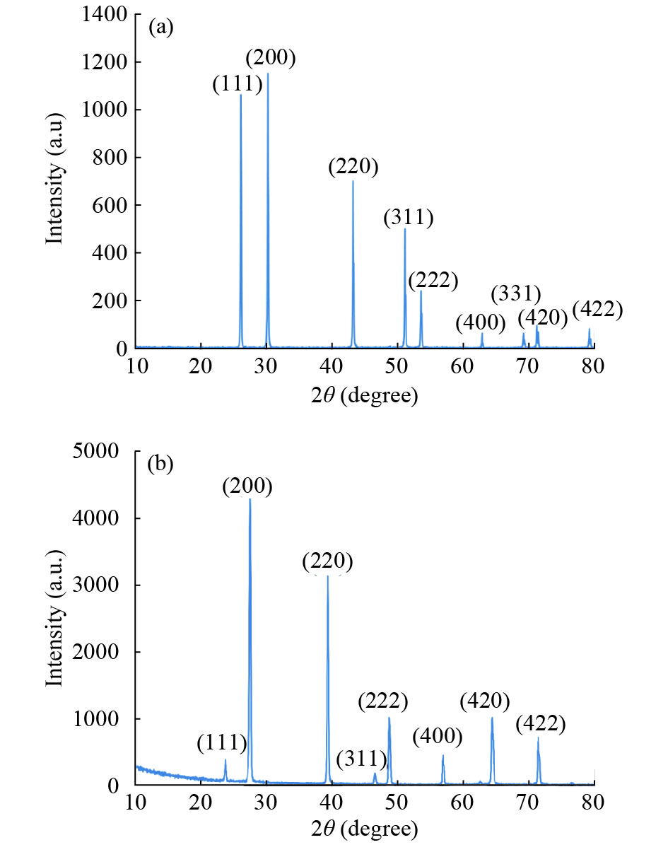
Fig. 1.
(Color online) XRD patterens of (a) PbS and (b) PbTe.
SEMICONDUCTOR MATERIALS
A. A. Azab1, , Azza A. Ward2, G. M. Mahmoud1, Eman M. El-Hanafy1, H. El-Zahed3 and F. S. Terra1
Corresponding author: A.A. Azab mail; aliazab@hotmail.com
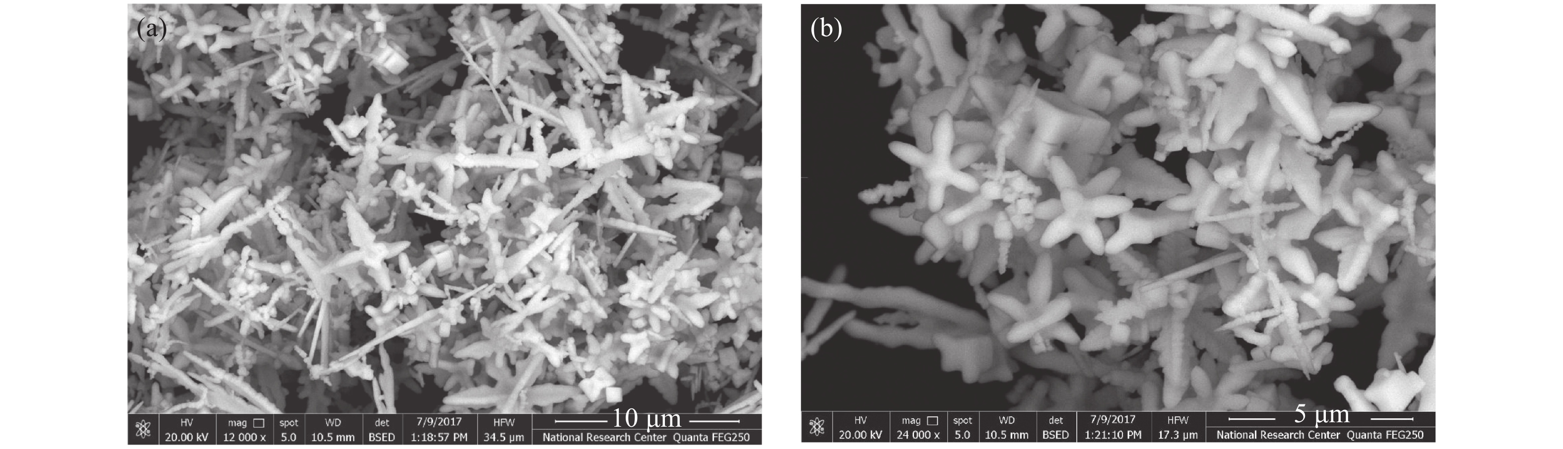
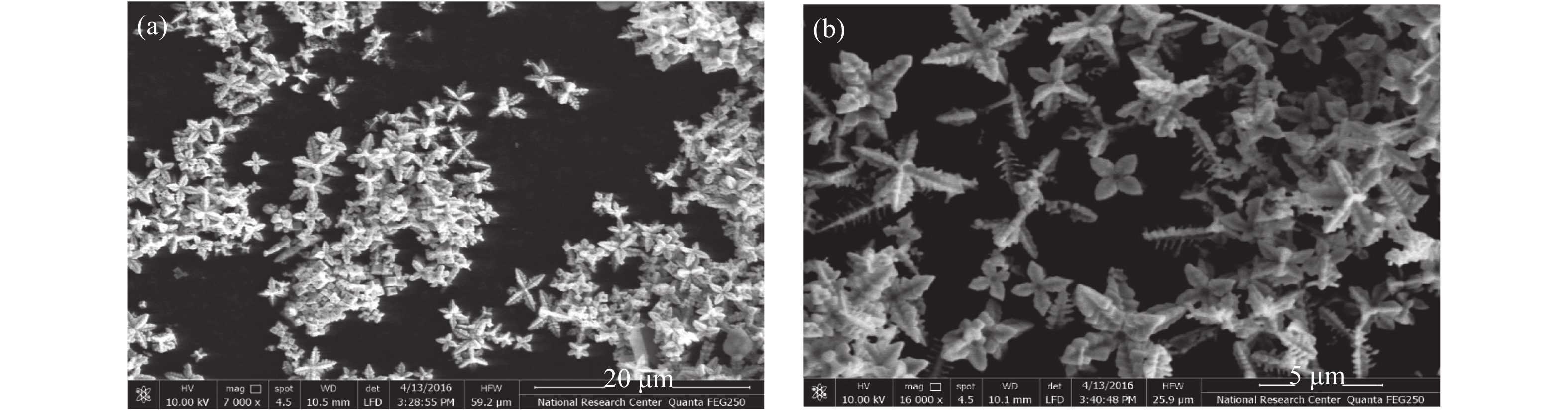
Abstract: In this work, PbS and PbTe nanomaterials with various morphologies were synthesized by a hydrothermal method. The structural properties were investigated by using X-ray diffraction (XRD) and corresponding scanning electron microscopy together with their EDX analysis. Both the PbS and PbTe nanomaterials possess good polycrystalline structure. The crystallite size, determined from the XRD data, of PbS is 5 nm whereas the corresponding value of PbTe is 2.69 nm. SEM micrographs reveal that the prepared PbS nanomaterial has star-shaped structures, micro-flowers, some cubes, and semi-dendrites, whereas PbTe has semi-flower structures. Additionally, the dielectric properties have been studied in a broad frequency range from 0.1 Hz up to 1 MHz at temperatures from 298–423 K. The real and imaginary parts of the complex dielectric constant ε' and ε'' of PbTe are comparatively higher than those of PbS. Moreover, the dielectric data were analyzed on the basis of the electric modulus.
Keywords: dielectric properties, PbS, PbTe, SEM, EDX, electric modulus
| [1] |
Yadav S, Pal R K, Sharma S K, et al. Determination of trap depth and trap density in Se70Te30−xZnx thin films using thermally stimulated current measurements. Physica B, 2009, 404: 2225 doi: 10.1016/j.physb.2009.04.015
|
| [2] |
Zakery A, Elliot S R. Optical properties and applications of chalcogenide glasses. J Non-Cryst Solids, 2003, 330: 1 doi: 10.1016/j.jnoncrysol.2003.08.064
|
| [3] |
Smith A W. Injection laser writing on chalcogenide films. Appl Opt, 1974, 13: 795 doi: 10.1364/AO.13.000795
|
| [4] |
Ohta T, Inoue K, Uchida M, et al. Phase change disk media having rapid cooling structure. Jpn J Appl Phys, 1989, 28: 123
|
| [5] |
Masoud S N, Ghanbari D, Logh M R, et al. Star-shaped PbS nanocrystals prepared by hydrothermal process in the presence of thioglycolic acid. Polyhedron, 2012, 35: 149 doi: 10.1016/j.poly.2012.01.010
|
| [6] |
Song C W, Sun M, Yin Y, et al. Synthesis of star-shaped lead sulfide (PbS) nanomaterials and their gas sensing properties. Mater Res, 2016, 19,6: 1351
|
| [7] |
Zhao Z H, Zhang K, Yang K, et al. Synthesis of size and shape controlled PbS nanocrystals and their self-assembly. Colloids and Surfaces A, 2010, 355: 114 doi: 10.1016/j.colsurfa.2009.12.009
|
| [8] |
Tohidi V, Jamshidi K, Namdar A, et al. Comparatve Studies on the structural, morphological, optical and electrical properties of nanocrystalline PbS thin films grown by using two different bath compositions. Mater Sci Semicond Process, 2014, 25: 197 doi: 10.1016/j.mssp.2013.11.028
|
| [9] |
Susan G, Masoud S, Bazarganipour M, et al. Novel precoursers for synthesis of dendrite-like PbTe nanostructures and investigation of photoluminescence behavior. Adv Powder Technol, 2014, 25(5): 1585 doi: 10.1016/j.apt.2014.05.007
|
| [10] |
Poudel B, Wang W Z, Wang D Z, et al. Shape evolution of lead telluride and selenide nanostructures under different hydrothermal synthesis conditons. J Nanosci Nanotechnol, 2006, 6: 1050 doi: 10.1166/jnn.2006.163
|
| [11] |
Chongjian Z, Shi Z, Ge B, Wang K, et al. Scalable solution-based synthesis of component-controllable ultrathin PbTe1−xSex nanowires with high n-type thermoelectric performance. J Mater Chem A, 2017, 5: 2876 doi: 10.1039/C6TA09189J
|
| [12] |
Kingumadevi L, Sathyamoorthy R. Synthesis of PbTe nanocubes, worm-like structures and nanoparticles by simple thermal evaporation method. Bull Mater Sci, 2013, 36,5: 771
|
| [13] |
Clemens B, Chen X, Narayanan R, et al. Chemistry and properties of nanocrystals of different shapes. Chem Rev, 2005, 105(4): 1025
|
| [14] |
Yadaiah K, Krishnaiah J, Vasudeva R, et al. Dielectric properties of (CdSe)1–x(ZnS)x mixed semiconductor compounds. Mater Sci Res Ind, 2012, 9(2): 179
|
| [15] |
Sedeek K, Adam A, Wahab L A, et al. Dielectric relaxation in Ge1–xSe2Pbx (x = 0, 0.2 and 0.6) nano-crystalline system. Mater Chem Phys, 2004, 85: 20 doi: 10.1016/j.matchemphys.2003.11.035
|
| [16] |
Anjali, Balbir S P, Suresh B, et al. On the AC-conductivity mechanism in nano-crystalline Se79–xTe15In6Pbx (x = 0, 1, 2, 4, 6, 8 and 10) alloys. Physica B, 2017, 523: 52 doi: 10.1016/j.physb.2017.08.001
|
| [17] |
Petrik P. Parameterization of the dielectric function of semiconductor nanocrystals. Physica B, 2014, 453,15: 2
|
| [18] |
Himpsel F J, Karlsson U O, McFeely F R, et al. Dielectrics on semiconductors. Mater Sci Eng B, 1988, 1(1): 9 doi: 10.1016/0921-5107(88)90025-6
|
| [19] |
El-Menyawy E M, Mahmoud G M, Gad S A, et al. Dependence of the structural, electrical and optical properties of PbSe nanomaterial prepared by hydrothermal method on the polyethylene glycol content. J Inorg Organomet Polym, 2015, 25: 1044 doi: 10.1007/s10904-015-0208-3
|
| [20] |
Azab A A, Sukrat A. Effect of grinding time on the structural and magnetic properties of ultrafine Ni0.7Zn0.3Fe2O4. J Ovon Res, 2015, 11: 195
|
| [21] |
Ahmed M A, Afify H H, ElZawawi I K, et al. Novel structural and magnetic properties of Mg doped copper nanoferrites prepared by conventional and wet methods. J Magnet Magnet Mater, 2012, 324: 2199 doi: 10.1016/j.jmmm.2012.02.025
|
| [22] |
Šalkus T, Kazakevičius E, Banys J, et al. Influence of grain size effect on electrical properties of Cu6PS5I superionic ceramics. Solid State Ion, 2014, 262: 597 doi: 10.1016/j.ssi.2013.10.040
|
| [23] |
Bellino M G, Lamas D G, Walsöe de Reca N E. Enhanced Ionic Conductivity in Nanostructured, Heavily Doped Ceria Ceramics. Adv Funct Mater, 2006, 16: 107 doi: 10.1002/(ISSN)1616-3028
|
| [24] |
Bellino M G, Lamas D G, Walsöe de Reca N E. A mechanism for the fast ionic transport in nanostructured oxide-ion solid electrolytes. Adv Mater, 2006, 18: 3005 doi: 10.1002/(ISSN)1521-4095
|
| [25] |
Jonscher A K. Understanding of the dielectric relaxation of solids. In: Physics of Thin Films. Ed by Hass, Francombe. New York: Academic, 1980, 11: 231
|
| [26] |
Taha T A, Azab A A. AC conductivity and dielectric properties of borotellurite glass. J Electron Mater, 2016, 45: 5170 doi: 10.1007/s11664-016-4749-1
|
| [27] |
Funke K. Jump relaxation in solid electrolytes. Prog Solid State Chem, 1993, 22: 111 doi: 10.1016/0079-6786(93)90002-9
|
| [28] |
Karthickprabhu S, Hirankumar G, Maheswaran A, et al. Structural and electrical studies on Zn2+ doped LiCoPO4. J Electrost, 2014, 72: 181 doi: 10.1016/j.elstat.2014.02.001
|
| [29] |
Murugavel S, Upadhyay M. Conduction in amorphous semiconductors. J Indian Inst Sci, 2011, 9: 1303
|
| [30] |
Elkony D. Electrical properties and conduction mechanism of Al-substituted Ni-Cdspinel ferrites. J Am Sci, 2012, 8: 8
|
| [31] |
Kumari N, Ghosh A, Bhattacharjee A. Investigation of structural and electrical transport mechanism of SnO2 with Al dopants. Indian J Phys, 2014, 88(10): 1059 doi: 10.1007/s12648-014-0514-6
|
| [32] |
Ahmed M A, Azab A A, El-Khawas E H, et al. Characterization and transport properties of mixed ferrite system Mn1–xCuxFe2O4; 0.0 ≤ x ≤ 0.7. Synthesis and Reactivity in Inorganic, Metal-Organic, and Nano-Metal Chemistry, 2016, 46: 376 doi: 10.1080/15533174.2014.988243
|
| [33] |
Adachi S. Optical constants of crystalline and amorphous semiconductors. New York: Springer Science & Business,1999
|
| [34] |
Ahmed M A, Azab A A, El-Khawas E H. Structural, magnetic and electrical properties of Bi doped LaFeO3 nano-crystals, synthesized by auto-combustion method. J Mater Sci, 2015, 26: 8765
|
| [35] |
Ashery A A, Zaki A H, Mourad H. Structural and frequency dependencies of a.c. and dielectric characterizations of epitaxial InSb-based heterojunctions. Bull Mater Sci, 2016, 39: 1057 doi: 10.1007/s12034-016-1224-9
|
| [36] |
Elliott S R. Temperature dependence of a.c. conductivity of chalcogenide glasses. Philos Mag B, 1978, 37: 553 doi: 10.1080/01418637808226448
|
| [37] |
Long A R. Frequency-dependent loss in amorphous semiconductors. Adv Phys, 1982, 31: 553 doi: 10.1080/00018738200101418
|
| [38] |
Gad S A, Moustafa A M, Ward A A. Preparation and some physical properties of Zn1−xCrxO. J Inorgan Organometal Polym Mater, 2015, 25: 1077 doi: 10.1007/s10904-015-0214-5
|
| [39] |
El-Nahass M M, Hassanien A M, Atta A A, et al. Ward electrical conductivity and dielectric relaxation of cerium (IV) oxide. J Mater Sci, 2017, 28: 1501
|
| [40] |
Ahmed M K, Mohammad L H, Azza A W. Novel nanofibrillated cellulose/polyvinylpyrrolidone/silver nanoparticles films with electrical conductivity properties. Carbohydrate Polymers, 2017, 157: 503 doi: 10.1016/j.carbpol.2016.10.008
|
| [41] |
Ahmed M N, Abd El-Khalek H M, El-Nahass M M. Dielectric and electric modulus studies on Ni (II)tetraphenyl porphyrin thin films. Org Opto-Elect, 2015, 1(1): 25
|
| [42] |
Macedo P B, Moynihan C T, Bose R. Role of ionic diffusion in polarization in vitreous ionic conductors. J Phys Chem Glass, 1972, 13: 171
|
| [43] |
Suriani I, Siti M M, Meng Ng, et al. Conductivity and dielectric behavior of PEO-based solid nanocomposite polymer electrolytes. Solid State Commun, 2012, 152: 426 doi: 10.1016/j.ssc.2011.11.037
|
| [44] |
Baskaran R, Selvasekarapandian S, Hirankumar G, et al. Dielectric and conductivity relaxation in PVAc based polymer electrolytes. Ionics, 2004, 10: 129 doi: 10.1007/BF02410321
|
| [45] |
Dhankhar S, Kund R S, Dult M, et al. Electrical conductivity and modulus formulation in zinc modified bismuth boro-tellurite glasses. AIP Conference Proceedings, 2016, 1728(1): 2
|
| [46] |
Abdellatif M H, Azab A A, Moustafa A M. Dielectric spectroscopy of localized electrical charges in ferrite thin film. J Electron Maters, 2018, 47(1): 378 doi: 10.1007/s11664-017-5782-4
|
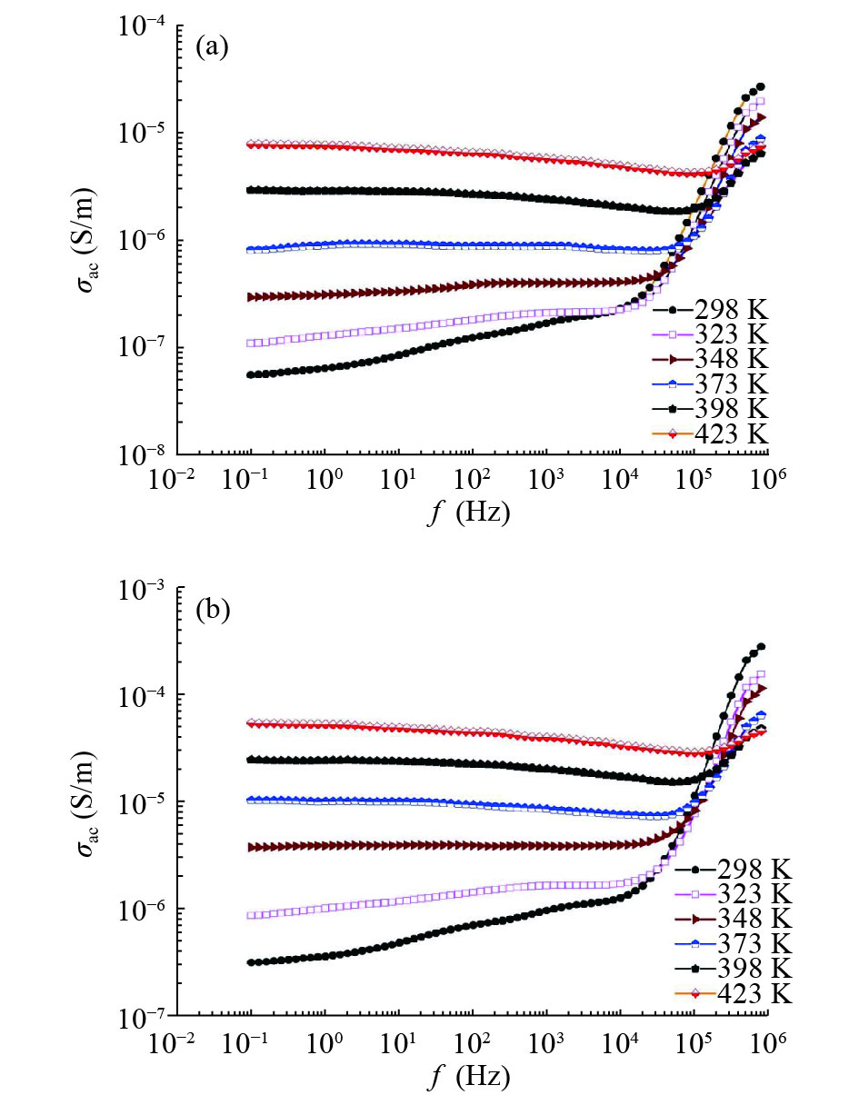
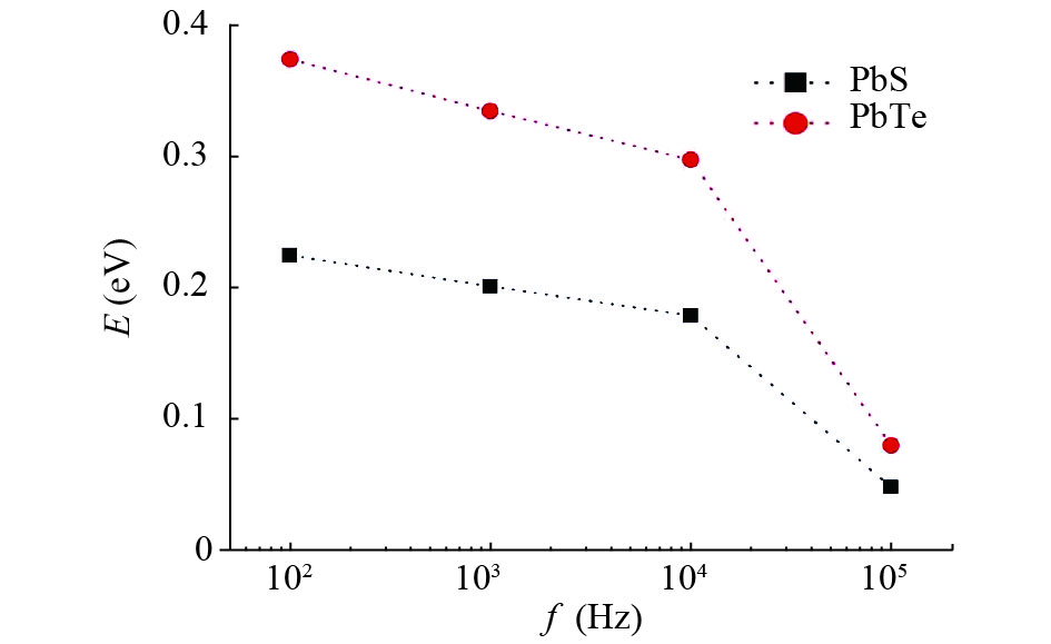
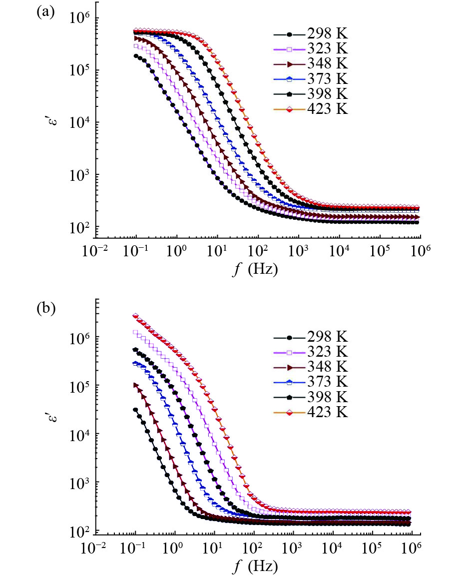
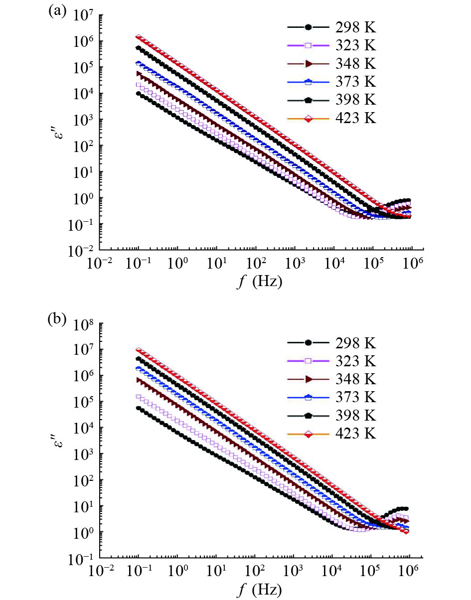
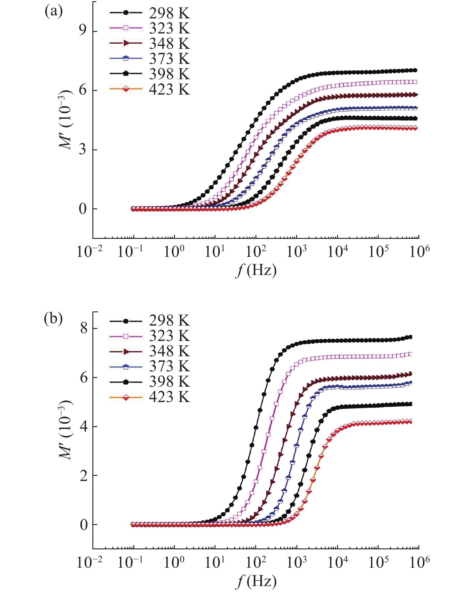
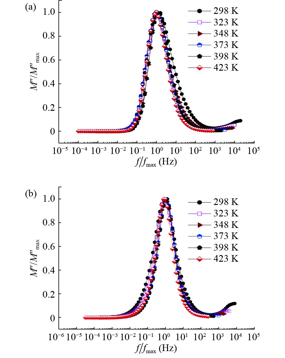
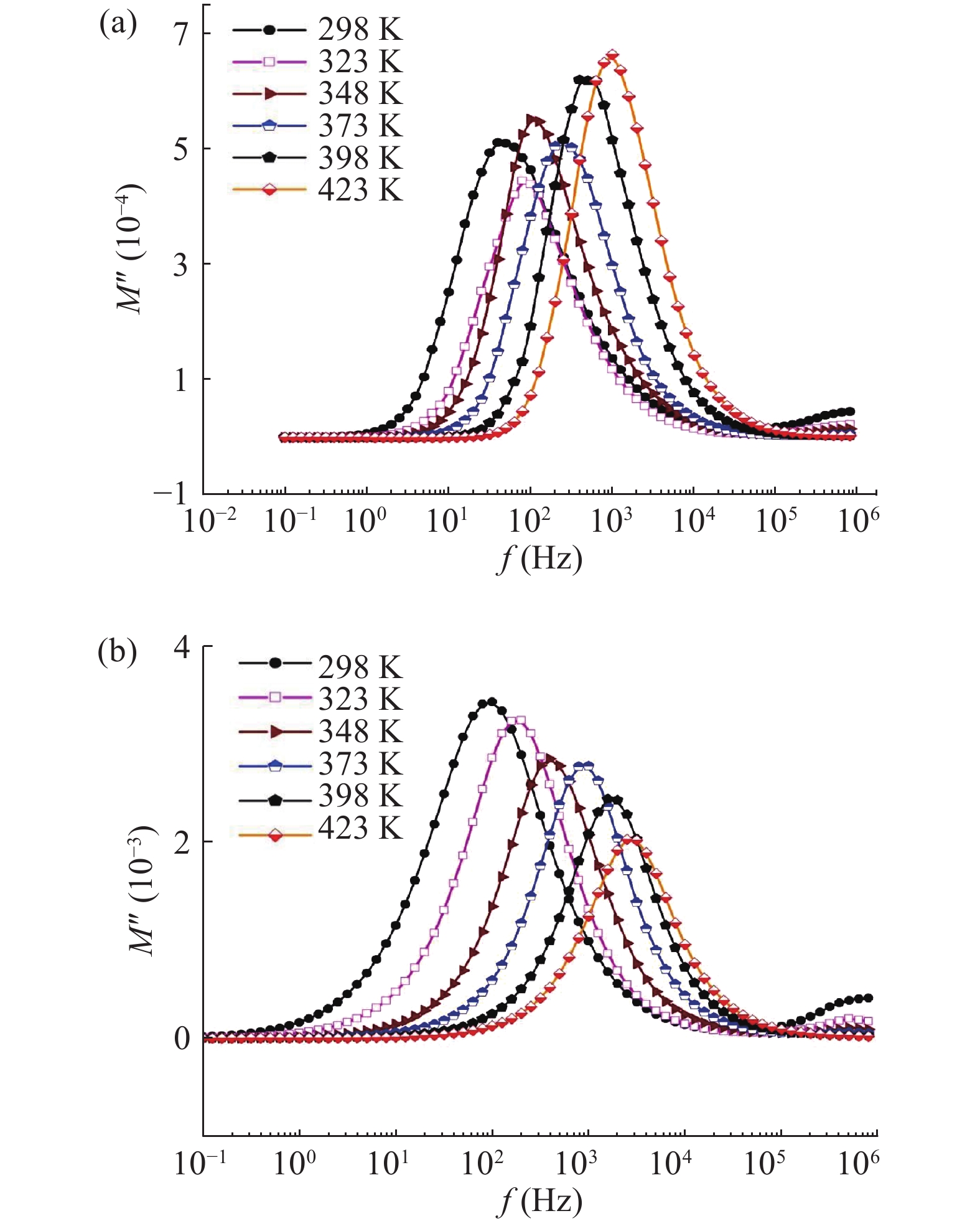
Table 1. Lattice parameter (a), average lattice parameter (aav.), crystallite size (D), average crystallite size (Dav.), strain (ϵ) and dislocation density (dd) for PbS and PbTe
| Parameter | a (Å) | aav. (Å) | D (nm) | Dav. (nm) | ϵ | dd |
| PbS | 5.91 | 5.92 | 5.00 | 6.01 | 0.0005 | 0.376 |
| PbTe | 6.47 | 6.57 | 2.69 | 1.95 | 0.0016 | 3.164 |
 DownLoad: CSV
Table 2. The frequency exponent (s), relaxation time (τm) and the Kohlraush exponentialparameters (β) for PbS and PbTe at different temperatures.
| T (K) | s | Tm | β | |||||
| PbS | PbTe | PbS | PbTe | PbS | PbTe | |||
| 298 | 1.28 | 1.40 | 6.05 × 10⁻³ | 2.41 × 10⁻³ | 0.12 | 0.24 | ||
| 323 | 1.23 | 1.17 | 3.03 × 10⁻³ | 1.21 × 10⁻³ | 0.24 | 0.30 | ||
| 348 | 0.95 | 1.24 | 2.41 × 10⁻³ | 6.09 × 10⁻⁴ | 0.19 | 0.31 | ||
| 373 | 0.89 | 0.86 | 9.57 × 10⁻⁴ | 3.05 × 10⁻⁴ | 0.24 | 0.31 | ||
| 398 | 0.48 | 0.58 | 6.09 × 10⁻⁴ | 1.53 × 10⁻⁴ | 0.19 | 0.31 | ||
| 423 | 0.25 | 0.24 | 2.43 × 10⁻⁴ | 7.64 × 10⁻⁴ | 0.31 | 0.39 | ||
DownLoad: CSV
| [1] |
Yadav S, Pal R K, Sharma S K, et al. Determination of trap depth and trap density in Se70Te30−xZnx thin films using thermally stimulated current measurements. Physica B, 2009, 404: 2225 doi: 10.1016/j.physb.2009.04.015
|
| [2] |
Zakery A, Elliot S R. Optical properties and applications of chalcogenide glasses. J Non-Cryst Solids, 2003, 330: 1 doi: 10.1016/j.jnoncrysol.2003.08.064
|
| [3] |
Smith A W. Injection laser writing on chalcogenide films. Appl Opt, 1974, 13: 795 doi: 10.1364/AO.13.000795
|
| [4] |
Ohta T, Inoue K, Uchida M, et al. Phase change disk media having rapid cooling structure. Jpn J Appl Phys, 1989, 28: 123
|
| [5] |
Masoud S N, Ghanbari D, Logh M R, et al. Star-shaped PbS nanocrystals prepared by hydrothermal process in the presence of thioglycolic acid. Polyhedron, 2012, 35: 149 doi: 10.1016/j.poly.2012.01.010
|
| [6] |
Song C W, Sun M, Yin Y, et al. Synthesis of star-shaped lead sulfide (PbS) nanomaterials and their gas sensing properties. Mater Res, 2016, 19,6: 1351
|
| [7] |
Zhao Z H, Zhang K, Yang K, et al. Synthesis of size and shape controlled PbS nanocrystals and their self-assembly. Colloids and Surfaces A, 2010, 355: 114 doi: 10.1016/j.colsurfa.2009.12.009
|
| [8] |
Tohidi V, Jamshidi K, Namdar A, et al. Comparatve Studies on the structural, morphological, optical and electrical properties of nanocrystalline PbS thin films grown by using two different bath compositions. Mater Sci Semicond Process, 2014, 25: 197 doi: 10.1016/j.mssp.2013.11.028
|
| [9] |
Susan G, Masoud S, Bazarganipour M, et al. Novel precoursers for synthesis of dendrite-like PbTe nanostructures and investigation of photoluminescence behavior. Adv Powder Technol, 2014, 25(5): 1585 doi: 10.1016/j.apt.2014.05.007
|
| [10] |
Poudel B, Wang W Z, Wang D Z, et al. Shape evolution of lead telluride and selenide nanostructures under different hydrothermal synthesis conditons. J Nanosci Nanotechnol, 2006, 6: 1050 doi: 10.1166/jnn.2006.163
|
| [11] |
Chongjian Z, Shi Z, Ge B, Wang K, et al. Scalable solution-based synthesis of component-controllable ultrathin PbTe1−xSex nanowires with high n-type thermoelectric performance. J Mater Chem A, 2017, 5: 2876 doi: 10.1039/C6TA09189J
|
| [12] |
Kingumadevi L, Sathyamoorthy R. Synthesis of PbTe nanocubes, worm-like structures and nanoparticles by simple thermal evaporation method. Bull Mater Sci, 2013, 36,5: 771
|
| [13] |
Clemens B, Chen X, Narayanan R, et al. Chemistry and properties of nanocrystals of different shapes. Chem Rev, 2005, 105(4): 1025
|
| [14] |
Yadaiah K, Krishnaiah J, Vasudeva R, et al. Dielectric properties of (CdSe)1–x(ZnS)x mixed semiconductor compounds. Mater Sci Res Ind, 2012, 9(2): 179
|
| [15] |
Sedeek K, Adam A, Wahab L A, et al. Dielectric relaxation in Ge1–xSe2Pbx (x = 0, 0.2 and 0.6) nano-crystalline system. Mater Chem Phys, 2004, 85: 20 doi: 10.1016/j.matchemphys.2003.11.035
|
| [16] |
Anjali, Balbir S P, Suresh B, et al. On the AC-conductivity mechanism in nano-crystalline Se79–xTe15In6Pbx (x = 0, 1, 2, 4, 6, 8 and 10) alloys. Physica B, 2017, 523: 52 doi: 10.1016/j.physb.2017.08.001
|
| [17] |
Petrik P. Parameterization of the dielectric function of semiconductor nanocrystals. Physica B, 2014, 453,15: 2
|
| [18] |
Himpsel F J, Karlsson U O, McFeely F R, et al. Dielectrics on semiconductors. Mater Sci Eng B, 1988, 1(1): 9 doi: 10.1016/0921-5107(88)90025-6
|
| [19] |
El-Menyawy E M, Mahmoud G M, Gad S A, et al. Dependence of the structural, electrical and optical properties of PbSe nanomaterial prepared by hydrothermal method on the polyethylene glycol content. J Inorg Organomet Polym, 2015, 25: 1044 doi: 10.1007/s10904-015-0208-3
|
| [20] |
Azab A A, Sukrat A. Effect of grinding time on the structural and magnetic properties of ultrafine Ni0.7Zn0.3Fe2O4. J Ovon Res, 2015, 11: 195
|
| [21] |
Ahmed M A, Afify H H, ElZawawi I K, et al. Novel structural and magnetic properties of Mg doped copper nanoferrites prepared by conventional and wet methods. J Magnet Magnet Mater, 2012, 324: 2199 doi: 10.1016/j.jmmm.2012.02.025
|
| [22] |
Šalkus T, Kazakevičius E, Banys J, et al. Influence of grain size effect on electrical properties of Cu6PS5I superionic ceramics. Solid State Ion, 2014, 262: 597 doi: 10.1016/j.ssi.2013.10.040
|
| [23] |
Bellino M G, Lamas D G, Walsöe de Reca N E. Enhanced Ionic Conductivity in Nanostructured, Heavily Doped Ceria Ceramics. Adv Funct Mater, 2006, 16: 107 doi: 10.1002/(ISSN)1616-3028
|
| [24] |
Bellino M G, Lamas D G, Walsöe de Reca N E. A mechanism for the fast ionic transport in nanostructured oxide-ion solid electrolytes. Adv Mater, 2006, 18: 3005 doi: 10.1002/(ISSN)1521-4095
|
| [25] |
Jonscher A K. Understanding of the dielectric relaxation of solids. In: Physics of Thin Films. Ed by Hass, Francombe. New York: Academic, 1980, 11: 231
|
| [26] |
Taha T A, Azab A A. AC conductivity and dielectric properties of borotellurite glass. J Electron Mater, 2016, 45: 5170 doi: 10.1007/s11664-016-4749-1
|
| [27] |
Funke K. Jump relaxation in solid electrolytes. Prog Solid State Chem, 1993, 22: 111 doi: 10.1016/0079-6786(93)90002-9
|
| [28] |
Karthickprabhu S, Hirankumar G, Maheswaran A, et al. Structural and electrical studies on Zn2+ doped LiCoPO4. J Electrost, 2014, 72: 181 doi: 10.1016/j.elstat.2014.02.001
|
| [29] |
Murugavel S, Upadhyay M. Conduction in amorphous semiconductors. J Indian Inst Sci, 2011, 9: 1303
|
| [30] |
Elkony D. Electrical properties and conduction mechanism of Al-substituted Ni-Cdspinel ferrites. J Am Sci, 2012, 8: 8
|
| [31] |
Kumari N, Ghosh A, Bhattacharjee A. Investigation of structural and electrical transport mechanism of SnO2 with Al dopants. Indian J Phys, 2014, 88(10): 1059 doi: 10.1007/s12648-014-0514-6
|
| [32] |
Ahmed M A, Azab A A, El-Khawas E H, et al. Characterization and transport properties of mixed ferrite system Mn1–xCuxFe2O4; 0.0 ≤ x ≤ 0.7. Synthesis and Reactivity in Inorganic, Metal-Organic, and Nano-Metal Chemistry, 2016, 46: 376 doi: 10.1080/15533174.2014.988243
|
| [33] |
Adachi S. Optical constants of crystalline and amorphous semiconductors. New York: Springer Science & Business,1999
|
| [34] |
Ahmed M A, Azab A A, El-Khawas E H. Structural, magnetic and electrical properties of Bi doped LaFeO3 nano-crystals, synthesized by auto-combustion method. J Mater Sci, 2015, 26: 8765
|
| [35] |
Ashery A A, Zaki A H, Mourad H. Structural and frequency dependencies of a.c. and dielectric characterizations of epitaxial InSb-based heterojunctions. Bull Mater Sci, 2016, 39: 1057 doi: 10.1007/s12034-016-1224-9
|
| [36] |
Elliott S R. Temperature dependence of a.c. conductivity of chalcogenide glasses. Philos Mag B, 1978, 37: 553 doi: 10.1080/01418637808226448
|
| [37] |
Long A R. Frequency-dependent loss in amorphous semiconductors. Adv Phys, 1982, 31: 553 doi: 10.1080/00018738200101418
|
| [38] |
Gad S A, Moustafa A M, Ward A A. Preparation and some physical properties of Zn1−xCrxO. J Inorgan Organometal Polym Mater, 2015, 25: 1077 doi: 10.1007/s10904-015-0214-5
|
| [39] |
El-Nahass M M, Hassanien A M, Atta A A, et al. Ward electrical conductivity and dielectric relaxation of cerium (IV) oxide. J Mater Sci, 2017, 28: 1501
|
| [40] |
Ahmed M K, Mohammad L H, Azza A W. Novel nanofibrillated cellulose/polyvinylpyrrolidone/silver nanoparticles films with electrical conductivity properties. Carbohydrate Polymers, 2017, 157: 503 doi: 10.1016/j.carbpol.2016.10.008
|
| [41] |
Ahmed M N, Abd El-Khalek H M, El-Nahass M M. Dielectric and electric modulus studies on Ni (II)tetraphenyl porphyrin thin films. Org Opto-Elect, 2015, 1(1): 25
|
| [42] |
Macedo P B, Moynihan C T, Bose R. Role of ionic diffusion in polarization in vitreous ionic conductors. J Phys Chem Glass, 1972, 13: 171
|
| [43] |
Suriani I, Siti M M, Meng Ng, et al. Conductivity and dielectric behavior of PEO-based solid nanocomposite polymer electrolytes. Solid State Commun, 2012, 152: 426 doi: 10.1016/j.ssc.2011.11.037
|
| [44] |
Baskaran R, Selvasekarapandian S, Hirankumar G, et al. Dielectric and conductivity relaxation in PVAc based polymer electrolytes. Ionics, 2004, 10: 129 doi: 10.1007/BF02410321
|
| [45] |
Dhankhar S, Kund R S, Dult M, et al. Electrical conductivity and modulus formulation in zinc modified bismuth boro-tellurite glasses. AIP Conference Proceedings, 2016, 1728(1): 2
|
| [46] |
Abdellatif M H, Azab A A, Moustafa A M. Dielectric spectroscopy of localized electrical charges in ferrite thin film. J Electron Maters, 2018, 47(1): 378 doi: 10.1007/s11664-017-5782-4
|


Article views: 5257 Times PDF downloads: 109 Times Cited by: 0 Times
Received: 20 July 2018 Revised: 15 September 2018 Online: Accepted Manuscript: 07 November 2018Uncorrected proof: 14 November 2018Published: 13 December 2018
| Citation: |
A. A. Azab, Azza A. Ward, G. M. Mahmoud, Eman M. El-Hanafy, H. El-Zahed, F. S. Terra. Structural and dielectric properties of prepared PbS and PbTe nanomaterials[J]. Journal of Semiconductors, 2018, 39(12): 123006. doi: 10.1088/1674-4926/39/12/123006
****
A A Azab, A A Ward, G M Mahmoud, E M El-Hanafy, H El-Zahed, F S Terra, Structural and dielectric properties of prepared PbS and PbTe nanomaterials[J]. J. Semicond., 2018, 39(12): 123006. doi: 10.1088/1674-4926/39/12/123006.

|
| [1] |
Yadav S, Pal R K, Sharma S K, et al. Determination of trap depth and trap density in Se70Te30−xZnx thin films using thermally stimulated current measurements. Physica B, 2009, 404: 2225 doi: 10.1016/j.physb.2009.04.015
|
| [2] |
Zakery A, Elliot S R. Optical properties and applications of chalcogenide glasses. J Non-Cryst Solids, 2003, 330: 1 doi: 10.1016/j.jnoncrysol.2003.08.064
|
| [3] |
Smith A W. Injection laser writing on chalcogenide films. Appl Opt, 1974, 13: 795 doi: 10.1364/AO.13.000795
|
| [4] |
Ohta T, Inoue K, Uchida M, et al. Phase change disk media having rapid cooling structure. Jpn J Appl Phys, 1989, 28: 123
|
| [5] |
Masoud S N, Ghanbari D, Logh M R, et al. Star-shaped PbS nanocrystals prepared by hydrothermal process in the presence of thioglycolic acid. Polyhedron, 2012, 35: 149 doi: 10.1016/j.poly.2012.01.010
|
| [6] |
Song C W, Sun M, Yin Y, et al. Synthesis of star-shaped lead sulfide (PbS) nanomaterials and their gas sensing properties. Mater Res, 2016, 19,6: 1351
|
| [7] |
Zhao Z H, Zhang K, Yang K, et al. Synthesis of size and shape controlled PbS nanocrystals and their self-assembly. Colloids and Surfaces A, 2010, 355: 114 doi: 10.1016/j.colsurfa.2009.12.009
|
| [8] |
Tohidi V, Jamshidi K, Namdar A, et al. Comparatve Studies on the structural, morphological, optical and electrical properties of nanocrystalline PbS thin films grown by using two different bath compositions. Mater Sci Semicond Process, 2014, 25: 197 doi: 10.1016/j.mssp.2013.11.028
|
| [9] |
Susan G, Masoud S, Bazarganipour M, et al. Novel precoursers for synthesis of dendrite-like PbTe nanostructures and investigation of photoluminescence behavior. Adv Powder Technol, 2014, 25(5): 1585 doi: 10.1016/j.apt.2014.05.007
|
| [10] |
Poudel B, Wang W Z, Wang D Z, et al. Shape evolution of lead telluride and selenide nanostructures under different hydrothermal synthesis conditons. J Nanosci Nanotechnol, 2006, 6: 1050 doi: 10.1166/jnn.2006.163
|
| [11] |
Chongjian Z, Shi Z, Ge B, Wang K, et al. Scalable solution-based synthesis of component-controllable ultrathin PbTe1−xSex nanowires with high n-type thermoelectric performance. J Mater Chem A, 2017, 5: 2876 doi: 10.1039/C6TA09189J
|
| [12] |
Kingumadevi L, Sathyamoorthy R. Synthesis of PbTe nanocubes, worm-like structures and nanoparticles by simple thermal evaporation method. Bull Mater Sci, 2013, 36,5: 771
|
| [13] |
Clemens B, Chen X, Narayanan R, et al. Chemistry and properties of nanocrystals of different shapes. Chem Rev, 2005, 105(4): 1025
|
| [14] |
Yadaiah K, Krishnaiah J, Vasudeva R, et al. Dielectric properties of (CdSe)1–x(ZnS)x mixed semiconductor compounds. Mater Sci Res Ind, 2012, 9(2): 179
|
| [15] |
Sedeek K, Adam A, Wahab L A, et al. Dielectric relaxation in Ge1–xSe2Pbx (x = 0, 0.2 and 0.6) nano-crystalline system. Mater Chem Phys, 2004, 85: 20 doi: 10.1016/j.matchemphys.2003.11.035
|
| [16] |
Anjali, Balbir S P, Suresh B, et al. On the AC-conductivity mechanism in nano-crystalline Se79–xTe15In6Pbx (x = 0, 1, 2, 4, 6, 8 and 10) alloys. Physica B, 2017, 523: 52 doi: 10.1016/j.physb.2017.08.001
|
| [17] |
Petrik P. Parameterization of the dielectric function of semiconductor nanocrystals. Physica B, 2014, 453,15: 2
|
| [18] |
Himpsel F J, Karlsson U O, McFeely F R, et al. Dielectrics on semiconductors. Mater Sci Eng B, 1988, 1(1): 9 doi: 10.1016/0921-5107(88)90025-6
|
| [19] |
El-Menyawy E M, Mahmoud G M, Gad S A, et al. Dependence of the structural, electrical and optical properties of PbSe nanomaterial prepared by hydrothermal method on the polyethylene glycol content. J Inorg Organomet Polym, 2015, 25: 1044 doi: 10.1007/s10904-015-0208-3
|
| [20] |
Azab A A, Sukrat A. Effect of grinding time on the structural and magnetic properties of ultrafine Ni0.7Zn0.3Fe2O4. J Ovon Res, 2015, 11: 195
|
| [21] |
Ahmed M A, Afify H H, ElZawawi I K, et al. Novel structural and magnetic properties of Mg doped copper nanoferrites prepared by conventional and wet methods. J Magnet Magnet Mater, 2012, 324: 2199 doi: 10.1016/j.jmmm.2012.02.025
|
| [22] |
Šalkus T, Kazakevičius E, Banys J, et al. Influence of grain size effect on electrical properties of Cu6PS5I superionic ceramics. Solid State Ion, 2014, 262: 597 doi: 10.1016/j.ssi.2013.10.040
|
| [23] |
Bellino M G, Lamas D G, Walsöe de Reca N E. Enhanced Ionic Conductivity in Nanostructured, Heavily Doped Ceria Ceramics. Adv Funct Mater, 2006, 16: 107 doi: 10.1002/(ISSN)1616-3028
|
| [24] |
Bellino M G, Lamas D G, Walsöe de Reca N E. A mechanism for the fast ionic transport in nanostructured oxide-ion solid electrolytes. Adv Mater, 2006, 18: 3005 doi: 10.1002/(ISSN)1521-4095
|
| [25] |
Jonscher A K. Understanding of the dielectric relaxation of solids. In: Physics of Thin Films. Ed by Hass, Francombe. New York: Academic, 1980, 11: 231
|
| [26] |
Taha T A, Azab A A. AC conductivity and dielectric properties of borotellurite glass. J Electron Mater, 2016, 45: 5170 doi: 10.1007/s11664-016-4749-1
|
| [27] |
Funke K. Jump relaxation in solid electrolytes. Prog Solid State Chem, 1993, 22: 111 doi: 10.1016/0079-6786(93)90002-9
|
| [28] |
Karthickprabhu S, Hirankumar G, Maheswaran A, et al. Structural and electrical studies on Zn2+ doped LiCoPO4. J Electrost, 2014, 72: 181 doi: 10.1016/j.elstat.2014.02.001
|
| [29] |
Murugavel S, Upadhyay M. Conduction in amorphous semiconductors. J Indian Inst Sci, 2011, 9: 1303
|
| [30] |
Elkony D. Electrical properties and conduction mechanism of Al-substituted Ni-Cdspinel ferrites. J Am Sci, 2012, 8: 8
|
| [31] |
Kumari N, Ghosh A, Bhattacharjee A. Investigation of structural and electrical transport mechanism of SnO2 with Al dopants. Indian J Phys, 2014, 88(10): 1059 doi: 10.1007/s12648-014-0514-6
|
| [32] |
Ahmed M A, Azab A A, El-Khawas E H, et al. Characterization and transport properties of mixed ferrite system Mn1–xCuxFe2O4; 0.0 ≤ x ≤ 0.7. Synthesis and Reactivity in Inorganic, Metal-Organic, and Nano-Metal Chemistry, 2016, 46: 376 doi: 10.1080/15533174.2014.988243
|
| [33] |
Adachi S. Optical constants of crystalline and amorphous semiconductors. New York: Springer Science & Business,1999
|
| [34] |
Ahmed M A, Azab A A, El-Khawas E H. Structural, magnetic and electrical properties of Bi doped LaFeO3 nano-crystals, synthesized by auto-combustion method. J Mater Sci, 2015, 26: 8765
|
| [35] |
Ashery A A, Zaki A H, Mourad H. Structural and frequency dependencies of a.c. and dielectric characterizations of epitaxial InSb-based heterojunctions. Bull Mater Sci, 2016, 39: 1057 doi: 10.1007/s12034-016-1224-9
|
| [36] |
Elliott S R. Temperature dependence of a.c. conductivity of chalcogenide glasses. Philos Mag B, 1978, 37: 553 doi: 10.1080/01418637808226448
|
| [37] |
Long A R. Frequency-dependent loss in amorphous semiconductors. Adv Phys, 1982, 31: 553 doi: 10.1080/00018738200101418
|
| [38] |
Gad S A, Moustafa A M, Ward A A. Preparation and some physical properties of Zn1−xCrxO. J Inorgan Organometal Polym Mater, 2015, 25: 1077 doi: 10.1007/s10904-015-0214-5
|
| [39] |
El-Nahass M M, Hassanien A M, Atta A A, et al. Ward electrical conductivity and dielectric relaxation of cerium (IV) oxide. J Mater Sci, 2017, 28: 1501
|
| [40] |
Ahmed M K, Mohammad L H, Azza A W. Novel nanofibrillated cellulose/polyvinylpyrrolidone/silver nanoparticles films with electrical conductivity properties. Carbohydrate Polymers, 2017, 157: 503 doi: 10.1016/j.carbpol.2016.10.008
|
| [41] |
Ahmed M N, Abd El-Khalek H M, El-Nahass M M. Dielectric and electric modulus studies on Ni (II)tetraphenyl porphyrin thin films. Org Opto-Elect, 2015, 1(1): 25
|
| [42] |
Macedo P B, Moynihan C T, Bose R. Role of ionic diffusion in polarization in vitreous ionic conductors. J Phys Chem Glass, 1972, 13: 171
|
| [43] |
Suriani I, Siti M M, Meng Ng, et al. Conductivity and dielectric behavior of PEO-based solid nanocomposite polymer electrolytes. Solid State Commun, 2012, 152: 426 doi: 10.1016/j.ssc.2011.11.037
|
| [44] |
Baskaran R, Selvasekarapandian S, Hirankumar G, et al. Dielectric and conductivity relaxation in PVAc based polymer electrolytes. Ionics, 2004, 10: 129 doi: 10.1007/BF02410321
|
| [45] |
Dhankhar S, Kund R S, Dult M, et al. Electrical conductivity and modulus formulation in zinc modified bismuth boro-tellurite glasses. AIP Conference Proceedings, 2016, 1728(1): 2
|
| [46] |
Abdellatif M H, Azab A A, Moustafa A M. Dielectric spectroscopy of localized electrical charges in ferrite thin film. J Electron Maters, 2018, 47(1): 378 doi: 10.1007/s11664-017-5782-4
|

 WeChat ID
Journal of Semiconductors © 2017 All Rights Reserved 京ICP备05085259号-2