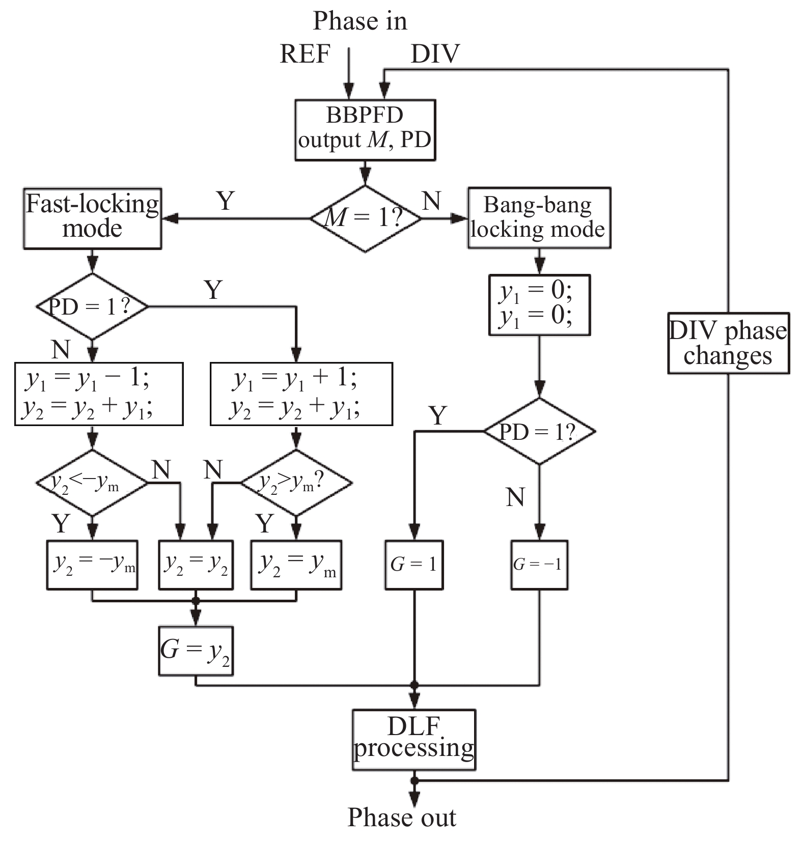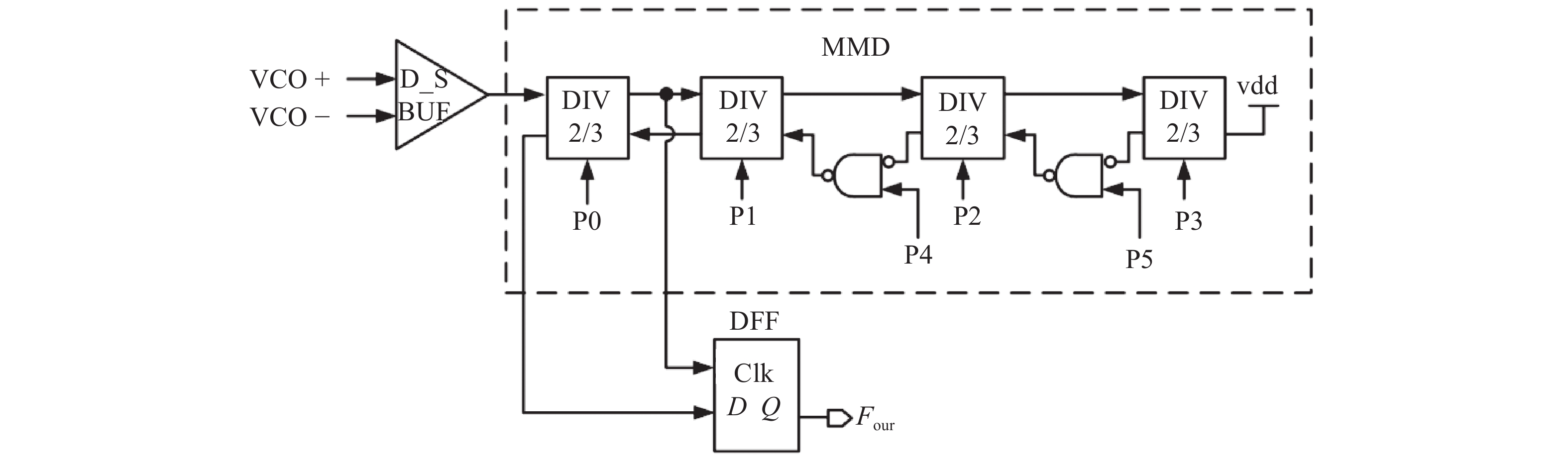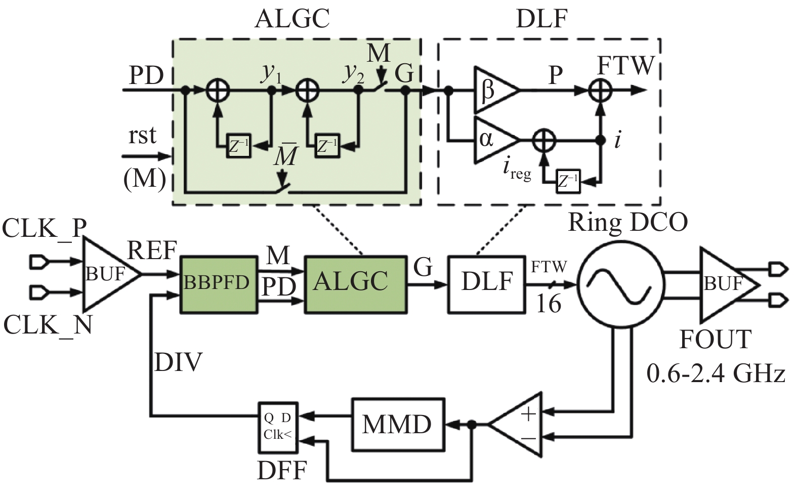
Fig. 1.
(Color online) Architecture of proposed fast-locking BBPLL.
SEMICONDUCTOR INTEGRATED CIRCUITS
Jincheng Yang1, 2, Zhao Zhang1, 2, Nan Qi1, 2, Liyuan Liu1, 2, , Jian Liu1, 2 and Nanjian Wu1, 2,
Corresponding author: Liyuan Liu, Email: liuly@semi.ac.cn; Nanjian Wu, nanjian@red.semi.ac.cn
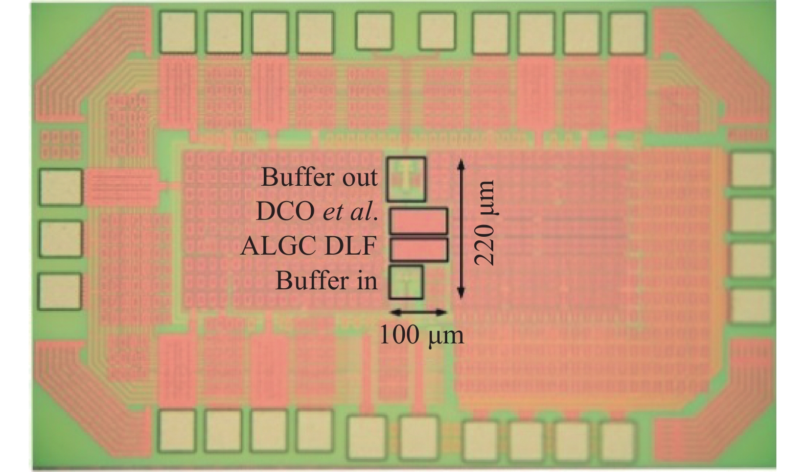
Abstract: This paper proposes a fast-locking bang-bang phase-locked loop (BBPLL). A novel adaptive loop gain controller (ALGC) is proposed to increase the locking speed of the BBPLL. A novel bang-bang phase/frequency detector (BBPFD) with adaptive-mode-selective circuits is proposed to select the locking mode of the BBPLL during the locking process. Based on the detected results of the BBPFD, the ALGC can dynamically adjust the overall gain of the loop for fast-locking procedure. Compared with the conventional BBPFD, only a few gates are added in the proposed BBPFD. Therefore, the proposed BBPFD with adaptive-mode-selective circuits is realized with little area and power penalties. The fast-locking BBPLL is implemented in a 65 nm CMOS technology. The core area of the BBPLL is 0.022 mm2. Measured results show that the BBPLL operates at a frequency range from 0.6 to 2.4 GHz. When operating at 1.8 GHz, the power consumption is 3.1 mW with a 0.9-V supply voltage. With the proposed techniques, the BBPLL achieves a normalized locked time of 1.1 μs @ 100 MHz frequency jump. The figure-of-merit of the fast-locking BBPLL is −334 dB.
Keywords: BBPLL, fast-locking, adaptive loop gain controller (ALGC), ADPLL, BBPFD, BBPD
| [1] |
Liu W Y, Chen J J, Liu X D, et al. A 2.4 GHz low power CMOS transceiver for LR-WPAN applications. Sci Chin Inform Sci, 2014, 57(8): 1
|
| [2] |
Chi B Y C, Song Z, Kuang L X, et al. CMOS mm-wave transceivers for Gbps wireless communication. J Semicond, 2016, 37(7): 071001 doi: 10.1088/1674-4926/37/7/071001
|
| [3] |
Doris K, Janssen E, Nani C, et al. A 480 mW 2.6 GS/s 10b time-interleaved ADC with 48.5 dB SNDR up to Nyquist in 65 nm CMOS. IEEE J Solid-State Circuits, 2011, 46(12): 2821 doi: 10.1109/JSSC.2011.2164961
|
| [4] |
Zhang X, Jiang H, Zhang L, et al. An energy-efficient ASIC for wireless body sensor networks in medical applications. IEEE Trans Biomed Circuits Syst, 2010, 4(1): 11 doi: 10.1109/TBCAS.2009.2031627
|
| [5] |
Elkholy A, Saxena S, Nandwana R K, et al. A 2.0–5.5 GHz wide bandwidth ring-based digital fractional-N PLL with extended range multi-modulus divider. IEEE J Solid-State Circuits, 2016, 51(8): 1771 doi: 10.1109/JSSC.2016.2557807
|
| [6] |
Liao D, Wang H, Dai F F, et al. An 802.11 a/b/g/n digital fractional-N PLL with automatic TDC linearity calibration for spur cancellation. IEEE J Solid-State Circuits, 2017, 52(5): 1210 doi: 10.1109/JSSC.2016.2638882
|
| [7] |
Wu Y, Shahmohammadi M, Chen Y, et al. A 3.5–6.8-GHz wide-bandwidth DTC-assisted fractional-N all-digital PLL with a MASH ΔΣ-TDC for low in-band phase noise. IEEE J Solid-State Circuits, 2017, 52(7): 1885 doi: 10.1109/JSSC.2017.2682841
|
| [8] |
Xu H, Abidi A A. Design methodology for phase-locked loops using binary (bang-bang) phase detectors. IEEE Trans Circuits Syst I, 2017, 64(7): 1637 doi: 10.1109/TCSI.2017.2679683
|
| [9] |
Kuan T K, Liu S I. A bang bang phase-locked loop using automatic loop gain control and loop latency reduction techniques. IEEE J Solid-State Circuits, 2016, 51(4): 821 doi: 10.1109/JSSC.2016.2519391
|
| [10] |
Elkholy A, Elmallah A, Elzeftawi M, et al. A 6.75-to-8.25 GHz, 250 fs rms-integrated-jitter 3.25 mW rapid on/off PVT-insensitive fractional-N injection-locked clock multiplier in 65 nm CMOS. Proc IEEE ISSCC Dig Tech Papers, San Francisco, 2016: 192
|
| [11] |
Nonis R, Grollitsch W, Santa T, et al. digPLL-Lite: A low-complexity, low-jitter fractional-N digital PLL architecture. IEEE J Solid-State Circuits, 2013, 48(12): 3134 doi: 10.1109/JSSC.2013.2272340
|
| [12] |
Marucci G, Levantino S, Maffezzoni P, et al. Analysis and design of low-jitter digital bang-bang phase-locked loops. IEEE Trans Circuits Syst I, 2014, 61(1): 26 doi: 10.1109/TCSI.2013.2268514
|
| [13] |
Huang Q, Zhan C, Burm J. A low-complexity fast-locking digital PLL with multi-output bang-bang phase detector. IEEE Asia Pacific Conference on Circuits and Systems (APCCAS), 2016: 418
|
| [14] |
Lin J M, Yang C Y. A fast-locking all-digital phase-locked loop with dynamic loop bandwidth adjustment. IEEE Trans Circuits Syst I, 2015, 62(10): 2411 doi: 10.1109/TCSI.2015.2477575
|
| [15] |
Lotfy A, Ghoneima M, Abdel-Moneum M. A fast locking hybrid TDC-BB ADPLL utilizing proportional derivative digital loop filter and power gated DCO. IEEE International Symposium on Circuits and Systems (ISCAS), 2016: 1646
|
| [16] |
Hung C C, Liu S I. A 40-GHz fast-locked all-digital phase-locked loop using a modified bang-bang algorithm. IEEE Trans Circuits Systems II, 2011, 58(6): 321 doi: 10.1109/TCSII.2011.2149610
|
| [17] |
Bertulessi L, Grimaldi L, Dmytro C, et al. A low-phase-noise digital bang-bang PLL with fast lock over a wide lock range. Proc IEEE ISSCC Dig Tech Papers, San Francisco, 2018: 252
|
| [18] |
Paliwal P, Laad P, Sattineni M, et al. Tradeoffs between settling time and jitter in phase locked loops. IEEE 56th International Midwest Symposium on Circuits and Systems (MWSCAS), 2013: 746
|
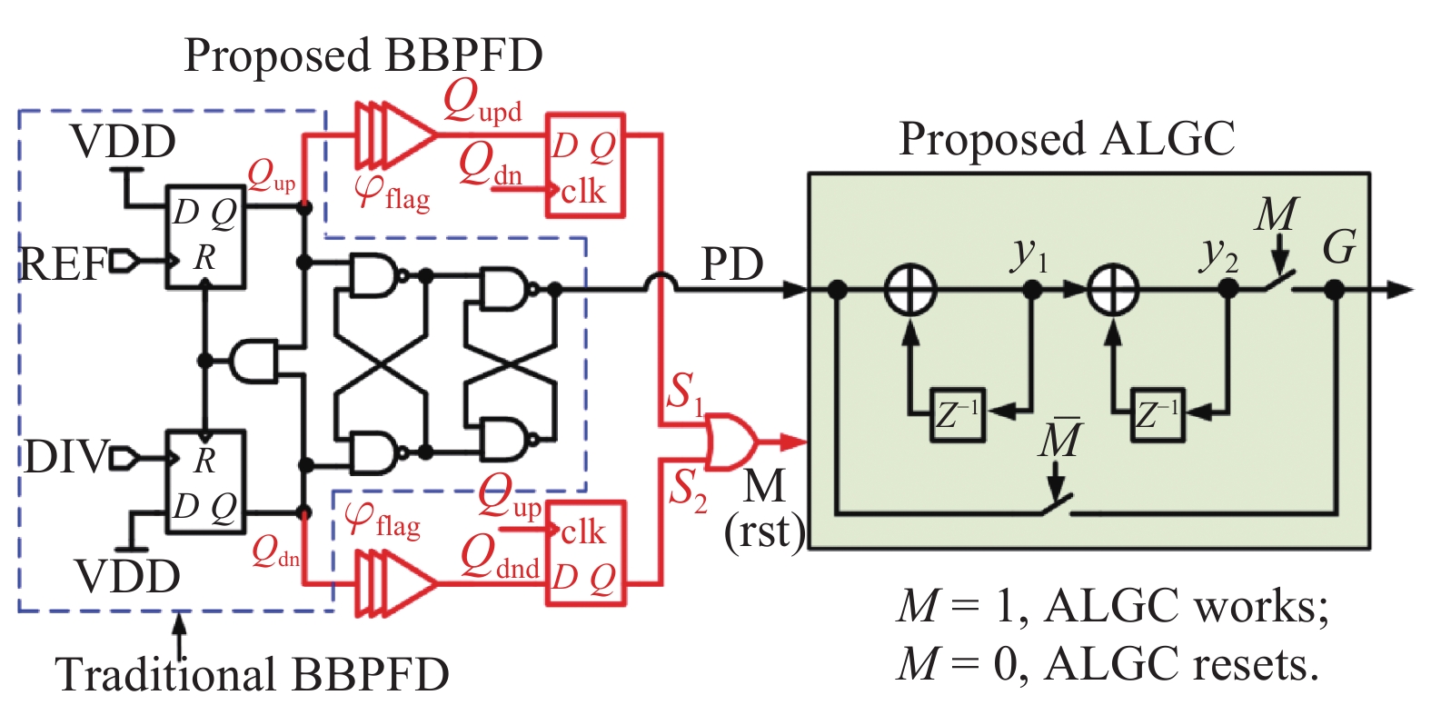
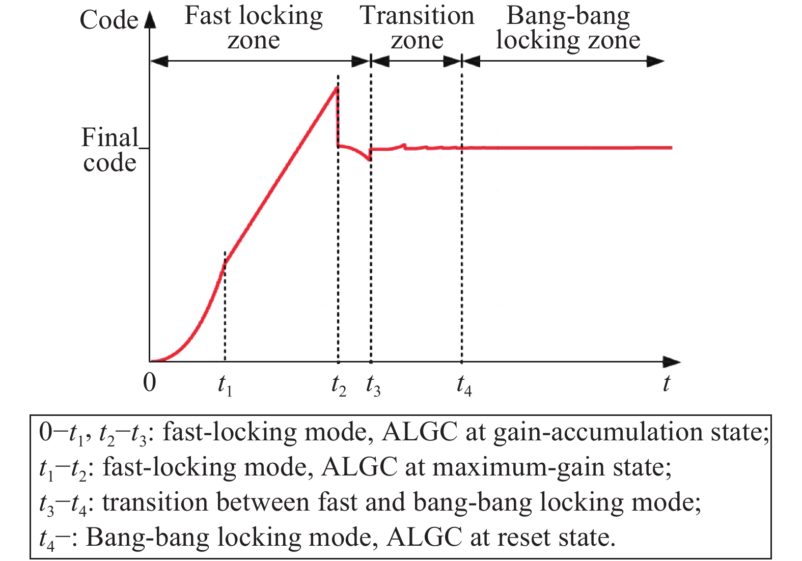
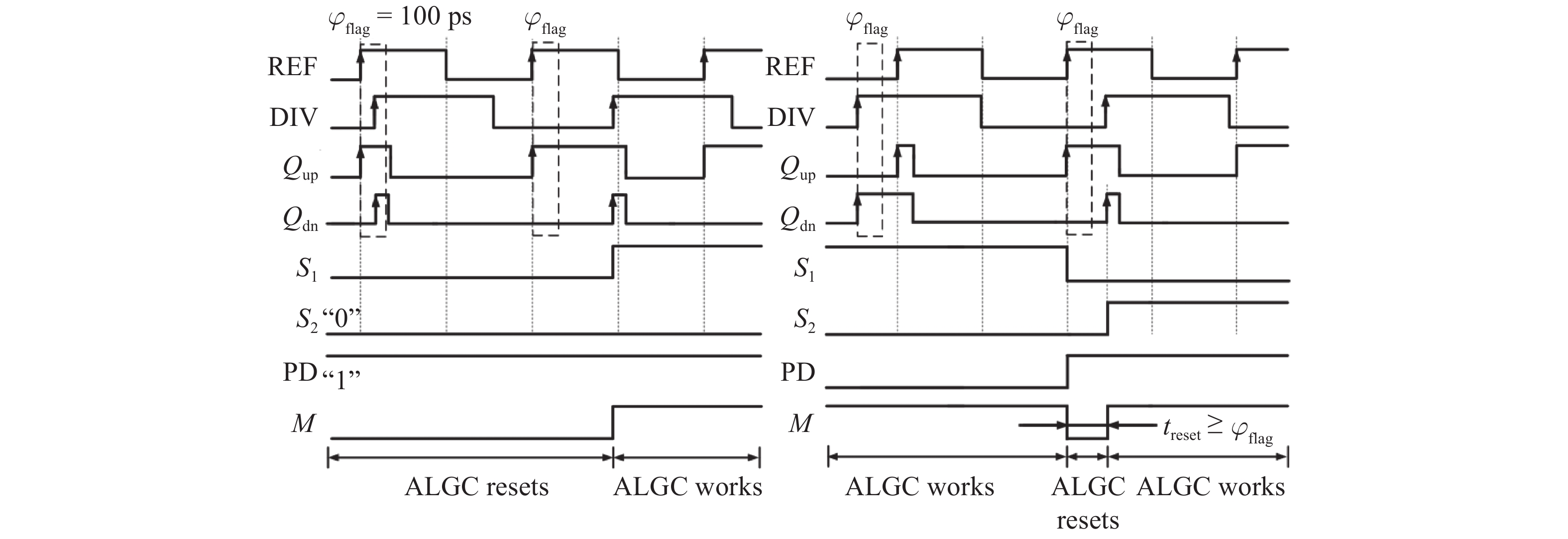
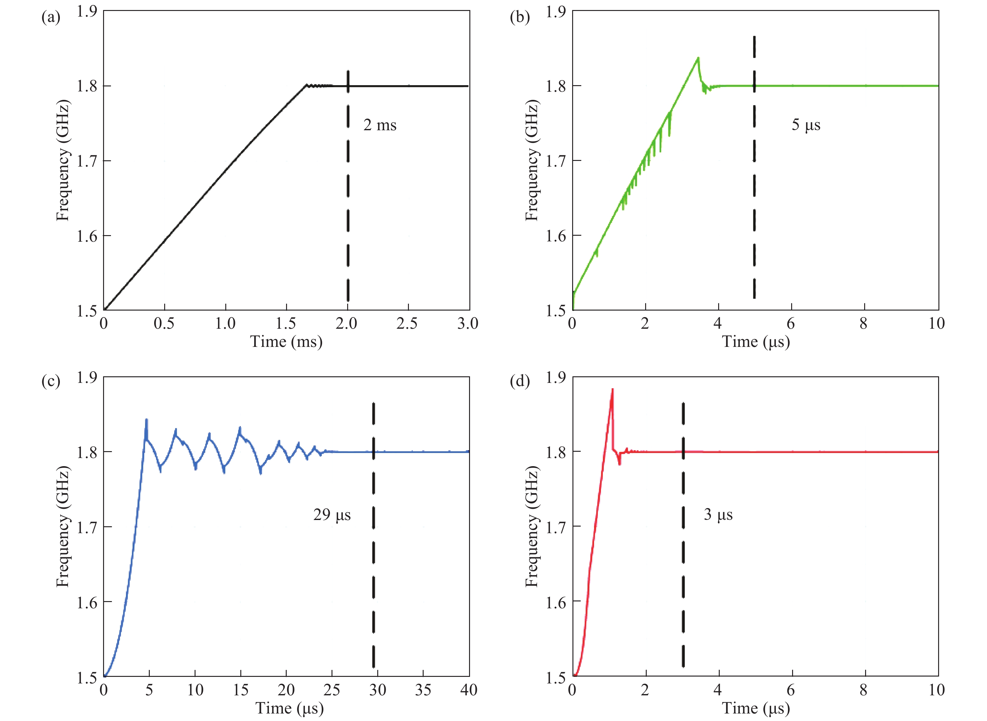
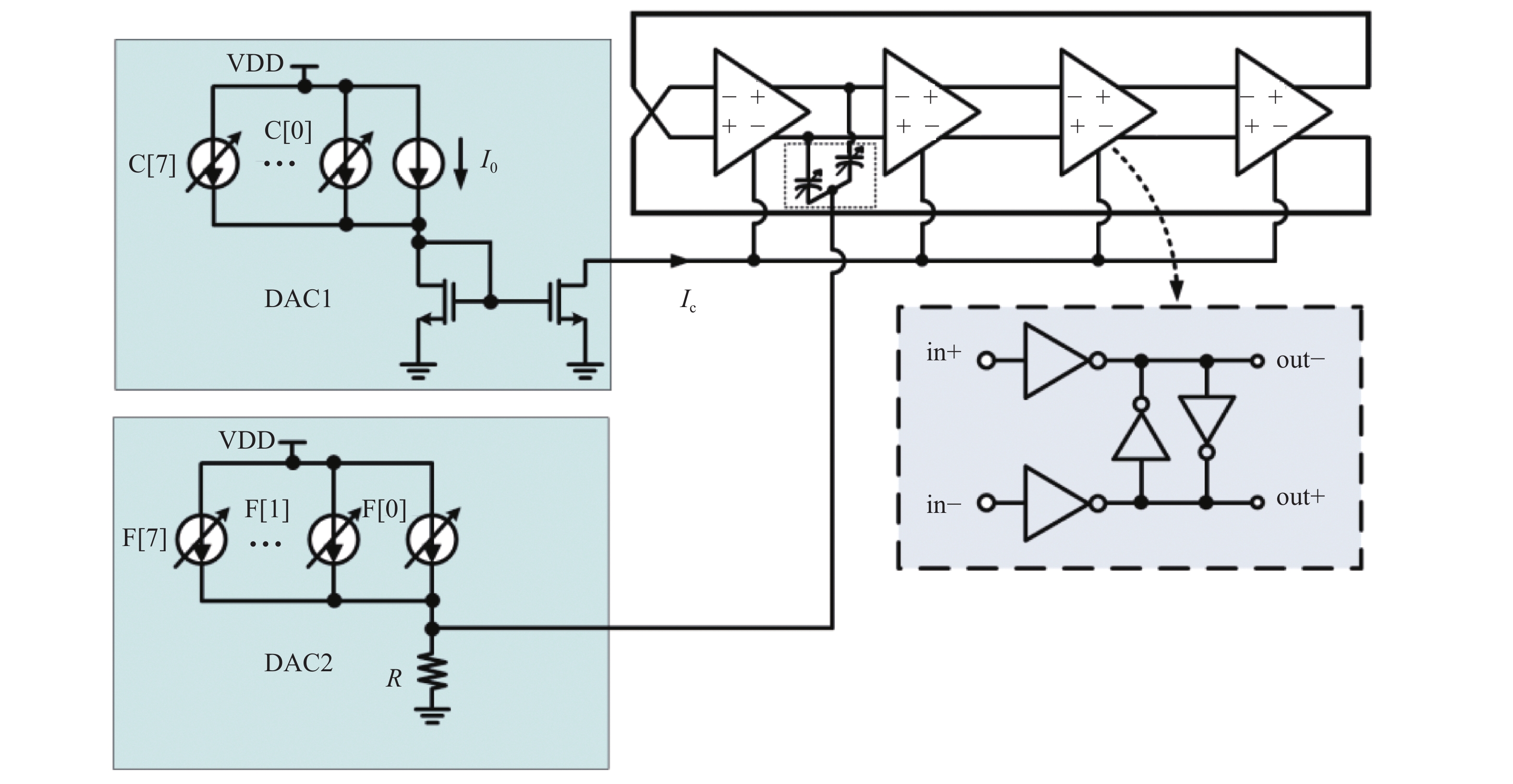
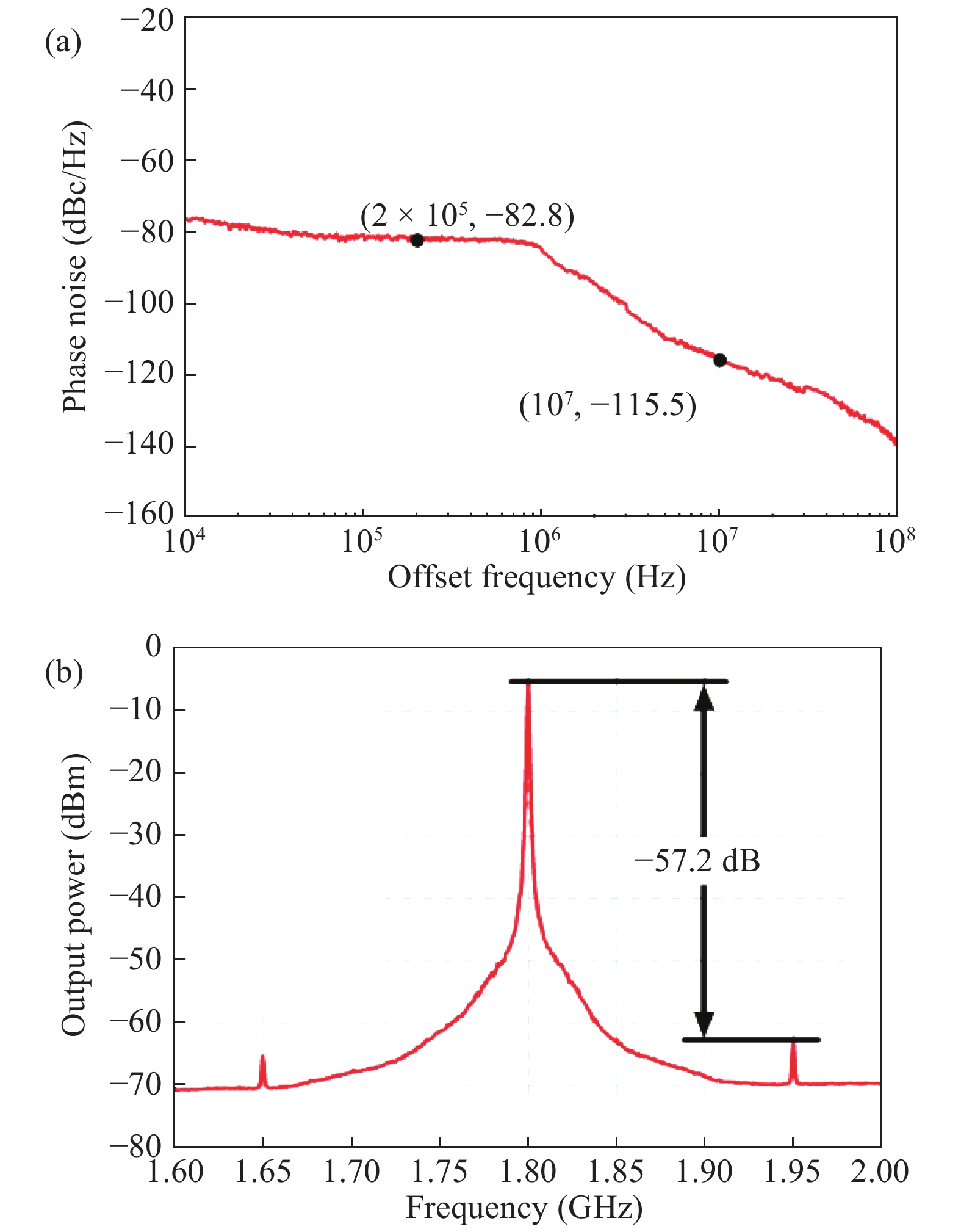
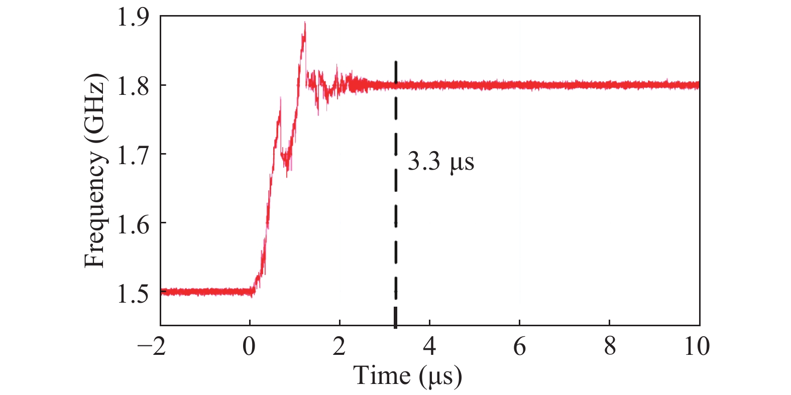
Table 1. Performances summary and comparisons.
| Parameter | This work | Ref. [13] | Ref. [14] | Ref. [16] | Ref. [17] |
| Technology (nm) | 65 | 180 | 180 | 90 | 65 |
| Type of DCO | Ring | Ring | Ring | LC | LC |
| Out. freq. (GHz) | 0.6 – 2.4 | 1.1 – 2.2 | 0.25 – 1.37 | 39 – 42 | 3.7 – 4.1 |
| Ref. freq. (MHz) | 150 | 11.1 | 19.5 | 156.25 | 52 |
| Area (mm2) | 0.022 | 0.42 | 0.77 | 0.3 | 0.61 |
| Power (mW) | 3.1 | 5.1 | 35 | 46 | 5.3 |
| RMS jitter (ps) | 10.3 | – | 8.9 | 0.3 | 0.18 |
| Ref. spur (dB) | −57.2 | – | −43.4 | −48.1 | – |
| Locked time (μs) (Freq. jump) | 3.3 (300 MHz) | 25 (400 MHz) | 2.9 (39 MHz) | 15 (50 MHz) | 5.6 (364 MHz) |
| Nor. locked time (μs @ 100 MHz) | 1.1 | 6.25 | 7.4 | 30 | 1.54 |
| FoM (dB) | −334.0 | – | −308.2 | −324.3 | −363.9 |
 DownLoad: CSV
| [1] |
Liu W Y, Chen J J, Liu X D, et al. A 2.4 GHz low power CMOS transceiver for LR-WPAN applications. Sci Chin Inform Sci, 2014, 57(8): 1
|
| [2] |
Chi B Y C, Song Z, Kuang L X, et al. CMOS mm-wave transceivers for Gbps wireless communication. J Semicond, 2016, 37(7): 071001 doi: 10.1088/1674-4926/37/7/071001
|
| [3] |
Doris K, Janssen E, Nani C, et al. A 480 mW 2.6 GS/s 10b time-interleaved ADC with 48.5 dB SNDR up to Nyquist in 65 nm CMOS. IEEE J Solid-State Circuits, 2011, 46(12): 2821 doi: 10.1109/JSSC.2011.2164961
|
| [4] |
Zhang X, Jiang H, Zhang L, et al. An energy-efficient ASIC for wireless body sensor networks in medical applications. IEEE Trans Biomed Circuits Syst, 2010, 4(1): 11 doi: 10.1109/TBCAS.2009.2031627
|
| [5] |
Elkholy A, Saxena S, Nandwana R K, et al. A 2.0–5.5 GHz wide bandwidth ring-based digital fractional-N PLL with extended range multi-modulus divider. IEEE J Solid-State Circuits, 2016, 51(8): 1771 doi: 10.1109/JSSC.2016.2557807
|
| [6] |
Liao D, Wang H, Dai F F, et al. An 802.11 a/b/g/n digital fractional-N PLL with automatic TDC linearity calibration for spur cancellation. IEEE J Solid-State Circuits, 2017, 52(5): 1210 doi: 10.1109/JSSC.2016.2638882
|
| [7] |
Wu Y, Shahmohammadi M, Chen Y, et al. A 3.5–6.8-GHz wide-bandwidth DTC-assisted fractional-N all-digital PLL with a MASH ΔΣ-TDC for low in-band phase noise. IEEE J Solid-State Circuits, 2017, 52(7): 1885 doi: 10.1109/JSSC.2017.2682841
|
| [8] |
Xu H, Abidi A A. Design methodology for phase-locked loops using binary (bang-bang) phase detectors. IEEE Trans Circuits Syst I, 2017, 64(7): 1637 doi: 10.1109/TCSI.2017.2679683
|
| [9] |
Kuan T K, Liu S I. A bang bang phase-locked loop using automatic loop gain control and loop latency reduction techniques. IEEE J Solid-State Circuits, 2016, 51(4): 821 doi: 10.1109/JSSC.2016.2519391
|
| [10] |
Elkholy A, Elmallah A, Elzeftawi M, et al. A 6.75-to-8.25 GHz, 250 fs rms-integrated-jitter 3.25 mW rapid on/off PVT-insensitive fractional-N injection-locked clock multiplier in 65 nm CMOS. Proc IEEE ISSCC Dig Tech Papers, San Francisco, 2016: 192
|
| [11] |
Nonis R, Grollitsch W, Santa T, et al. digPLL-Lite: A low-complexity, low-jitter fractional-N digital PLL architecture. IEEE J Solid-State Circuits, 2013, 48(12): 3134 doi: 10.1109/JSSC.2013.2272340
|
| [12] |
Marucci G, Levantino S, Maffezzoni P, et al. Analysis and design of low-jitter digital bang-bang phase-locked loops. IEEE Trans Circuits Syst I, 2014, 61(1): 26 doi: 10.1109/TCSI.2013.2268514
|
| [13] |
Huang Q, Zhan C, Burm J. A low-complexity fast-locking digital PLL with multi-output bang-bang phase detector. IEEE Asia Pacific Conference on Circuits and Systems (APCCAS), 2016: 418
|
| [14] |
Lin J M, Yang C Y. A fast-locking all-digital phase-locked loop with dynamic loop bandwidth adjustment. IEEE Trans Circuits Syst I, 2015, 62(10): 2411 doi: 10.1109/TCSI.2015.2477575
|
| [15] |
Lotfy A, Ghoneima M, Abdel-Moneum M. A fast locking hybrid TDC-BB ADPLL utilizing proportional derivative digital loop filter and power gated DCO. IEEE International Symposium on Circuits and Systems (ISCAS), 2016: 1646
|
| [16] |
Hung C C, Liu S I. A 40-GHz fast-locked all-digital phase-locked loop using a modified bang-bang algorithm. IEEE Trans Circuits Systems II, 2011, 58(6): 321 doi: 10.1109/TCSII.2011.2149610
|
| [17] |
Bertulessi L, Grimaldi L, Dmytro C, et al. A low-phase-noise digital bang-bang PLL with fast lock over a wide lock range. Proc IEEE ISSCC Dig Tech Papers, San Francisco, 2018: 252
|
| [18] |
Paliwal P, Laad P, Sattineni M, et al. Tradeoffs between settling time and jitter in phase locked loops. IEEE 56th International Midwest Symposium on Circuits and Systems (MWSCAS), 2013: 746
|


Article views: 7505 Times PDF downloads: 350 Times Cited by: 0 Times
Received: 06 April 2018 Revised: 04 May 2018 Online: Uncorrected proof: 04 July 2018Accepted Manuscript: 05 July 2018Corrected proof: 01 November 2018Published: 13 December 2018
| Citation: |
Jincheng Yang, Zhao Zhang, Nan Qi, Liyuan Liu, Jian Liu, Nanjian Wu. A fast-locking bang-bang phase-locked loop with adaptive loop gain controller[J]. Journal of Semiconductors, 2018, 39(12): 125002. doi: 10.1088/1674-4926/39/12/125002
****
J C Yang, Z Zhang, N Qi, L Y Liu, J Liu, N J Wu, A fast-locking bang-bang phase-locked loop with adaptive loop gain controller[J]. J. Semicond., 2018, 39(12): 125002. doi: 10.1088/1674-4926/39/12/125002.

|
| [1] |
Liu W Y, Chen J J, Liu X D, et al. A 2.4 GHz low power CMOS transceiver for LR-WPAN applications. Sci Chin Inform Sci, 2014, 57(8): 1
|
| [2] |
Chi B Y C, Song Z, Kuang L X, et al. CMOS mm-wave transceivers for Gbps wireless communication. J Semicond, 2016, 37(7): 071001 doi: 10.1088/1674-4926/37/7/071001
|
| [3] |
Doris K, Janssen E, Nani C, et al. A 480 mW 2.6 GS/s 10b time-interleaved ADC with 48.5 dB SNDR up to Nyquist in 65 nm CMOS. IEEE J Solid-State Circuits, 2011, 46(12): 2821 doi: 10.1109/JSSC.2011.2164961
|
| [4] |
Zhang X, Jiang H, Zhang L, et al. An energy-efficient ASIC for wireless body sensor networks in medical applications. IEEE Trans Biomed Circuits Syst, 2010, 4(1): 11 doi: 10.1109/TBCAS.2009.2031627
|
| [5] |
Elkholy A, Saxena S, Nandwana R K, et al. A 2.0–5.5 GHz wide bandwidth ring-based digital fractional-N PLL with extended range multi-modulus divider. IEEE J Solid-State Circuits, 2016, 51(8): 1771 doi: 10.1109/JSSC.2016.2557807
|
| [6] |
Liao D, Wang H, Dai F F, et al. An 802.11 a/b/g/n digital fractional-N PLL with automatic TDC linearity calibration for spur cancellation. IEEE J Solid-State Circuits, 2017, 52(5): 1210 doi: 10.1109/JSSC.2016.2638882
|
| [7] |
Wu Y, Shahmohammadi M, Chen Y, et al. A 3.5–6.8-GHz wide-bandwidth DTC-assisted fractional-N all-digital PLL with a MASH ΔΣ-TDC for low in-band phase noise. IEEE J Solid-State Circuits, 2017, 52(7): 1885 doi: 10.1109/JSSC.2017.2682841
|
| [8] |
Xu H, Abidi A A. Design methodology for phase-locked loops using binary (bang-bang) phase detectors. IEEE Trans Circuits Syst I, 2017, 64(7): 1637 doi: 10.1109/TCSI.2017.2679683
|
| [9] |
Kuan T K, Liu S I. A bang bang phase-locked loop using automatic loop gain control and loop latency reduction techniques. IEEE J Solid-State Circuits, 2016, 51(4): 821 doi: 10.1109/JSSC.2016.2519391
|
| [10] |
Elkholy A, Elmallah A, Elzeftawi M, et al. A 6.75-to-8.25 GHz, 250 fs rms-integrated-jitter 3.25 mW rapid on/off PVT-insensitive fractional-N injection-locked clock multiplier in 65 nm CMOS. Proc IEEE ISSCC Dig Tech Papers, San Francisco, 2016: 192
|
| [11] |
Nonis R, Grollitsch W, Santa T, et al. digPLL-Lite: A low-complexity, low-jitter fractional-N digital PLL architecture. IEEE J Solid-State Circuits, 2013, 48(12): 3134 doi: 10.1109/JSSC.2013.2272340
|
| [12] |
Marucci G, Levantino S, Maffezzoni P, et al. Analysis and design of low-jitter digital bang-bang phase-locked loops. IEEE Trans Circuits Syst I, 2014, 61(1): 26 doi: 10.1109/TCSI.2013.2268514
|
| [13] |
Huang Q, Zhan C, Burm J. A low-complexity fast-locking digital PLL with multi-output bang-bang phase detector. IEEE Asia Pacific Conference on Circuits and Systems (APCCAS), 2016: 418
|
| [14] |
Lin J M, Yang C Y. A fast-locking all-digital phase-locked loop with dynamic loop bandwidth adjustment. IEEE Trans Circuits Syst I, 2015, 62(10): 2411 doi: 10.1109/TCSI.2015.2477575
|
| [15] |
Lotfy A, Ghoneima M, Abdel-Moneum M. A fast locking hybrid TDC-BB ADPLL utilizing proportional derivative digital loop filter and power gated DCO. IEEE International Symposium on Circuits and Systems (ISCAS), 2016: 1646
|
| [16] |
Hung C C, Liu S I. A 40-GHz fast-locked all-digital phase-locked loop using a modified bang-bang algorithm. IEEE Trans Circuits Systems II, 2011, 58(6): 321 doi: 10.1109/TCSII.2011.2149610
|
| [17] |
Bertulessi L, Grimaldi L, Dmytro C, et al. A low-phase-noise digital bang-bang PLL with fast lock over a wide lock range. Proc IEEE ISSCC Dig Tech Papers, San Francisco, 2018: 252
|
| [18] |
Paliwal P, Laad P, Sattineni M, et al. Tradeoffs between settling time and jitter in phase locked loops. IEEE 56th International Midwest Symposium on Circuits and Systems (MWSCAS), 2013: 746
|

 WeChat ID
Journal of Semiconductors © 2017 All Rights Reserved 京ICP备05085259号-2