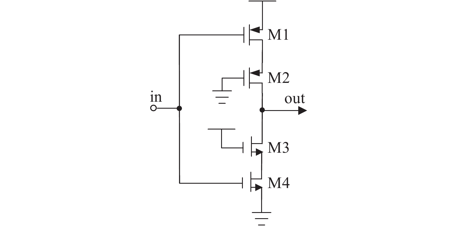
Fig. 1.
Integrator circuit (a) using OTA, (b) using inverter.
SEMICONDUCTOR INTEGRATED CIRCUITS
Chengying Chen and Hongyi Zhang
Corresponding author: Chengying Chen, Email: chenchengying363@163.com
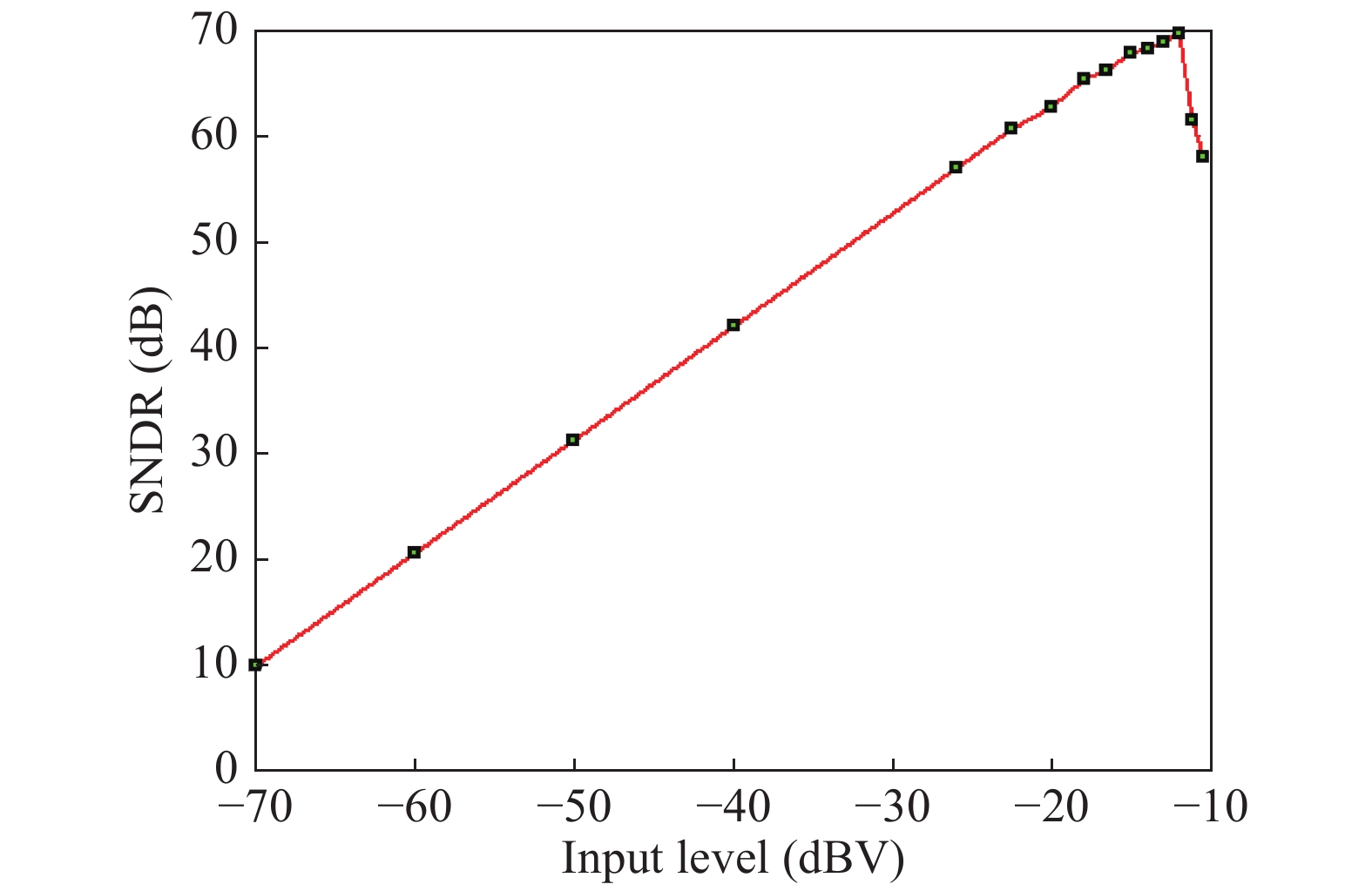
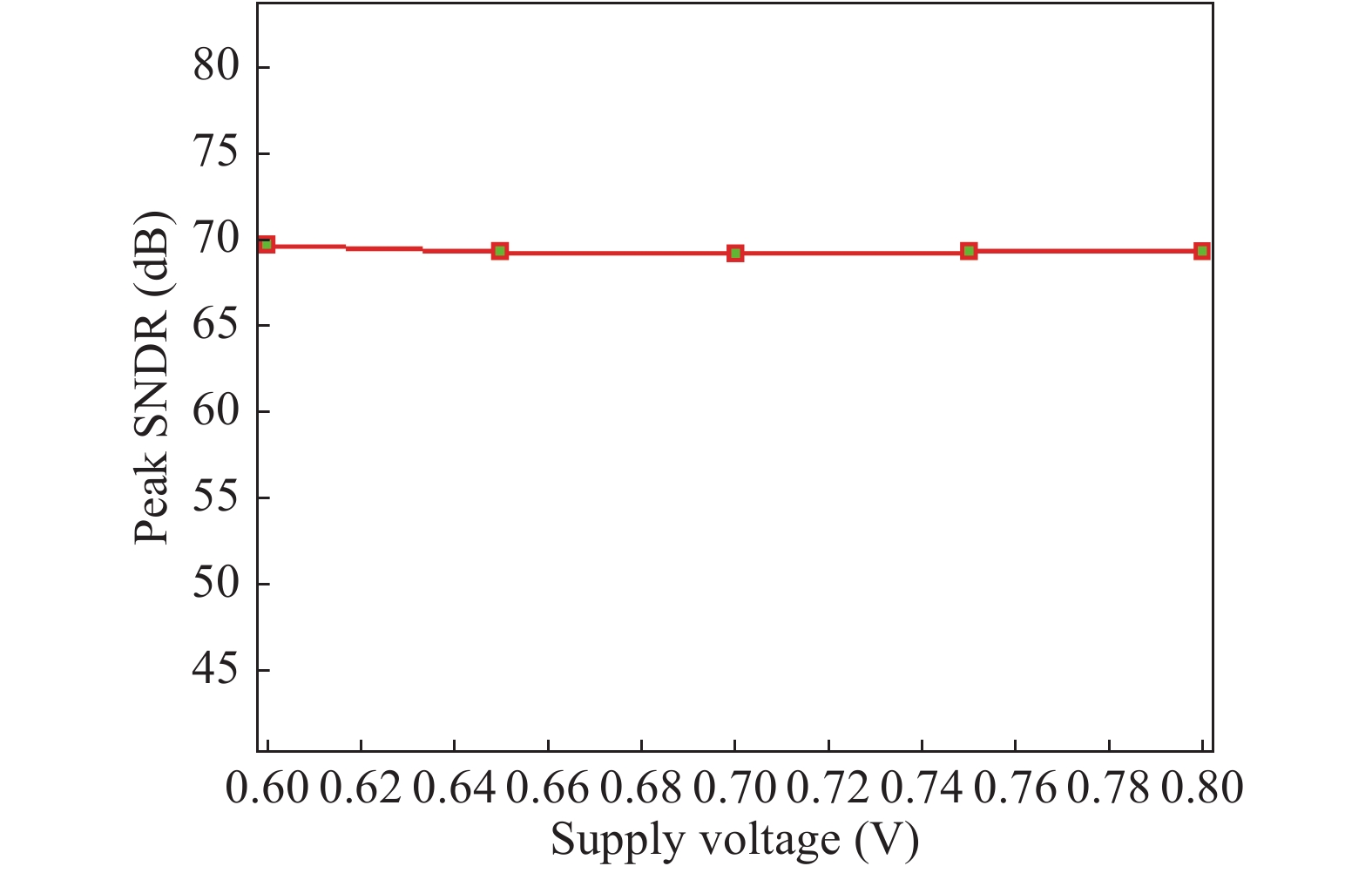
Abstract: In this paper a 0.6 V, 14 bit/500 Hz subthreshold inverter-based sigma–delta modulator is proposed. In the first integrator of the modulator, a bootstrap switch is used to accomplish accurate signal sampling. Without a transconductor operational amplifier (OTA), the sigma–delta modulator adopts a cascode inverter in the subthreshold region to save power consumption. The modulator is fabricated with a 0.13 μm CMOS mixed-signal process. The experiment results show that with the 0.6 V power supply it achieves a maximum SNDR of 69.7 dB and an ENOB of 11.3 bit, respectively, but only consumes 5.07 μw power dissipation.
Keywords: subthreshold, sigma–delta modulator, inverter, bootstrap switch
| [1] |
Wang Y C, Ke K R, W H Q, et al. A low power low noise analog front end for portable healthcare system. J Semicond, 2015, 36(10): 105008 doi: 10.1088/1674-4926/36/10/105008
|
| [2] |
Mao Y Q, Gao T Q, Xu X D, et al. A fully integrated CMOS super-regenerative wake-up receiver for EEG applications. J Semicond, 2016, 37(9): 095001 doi: 10.1088/1674-4926/37/9/095001
|
| [3] |
Xiao G L, Qin Y L, Xu W L, et al. Demonstration of a fully differential VGA chip with small THD for ECG acquisition system. J Semicond, 2015, 36(10): 105005 doi: 10.1088/1674-4926/36/10/105005
|
| [4] |
Panigrahi A, Parhi A. A 0.5-V body driven pseudo-differential OTA for low voltage and low power applications. IEEE India Conference (INDICON), 2015: 1
|
| [5] |
Zhao X K, Song Z, Chi B Y. A 60-dB DR PGA with DC-offset calibration for short-distance wireless receiver. IEEE International Symposium on VLSI design, Automation and Test (VLSI-DAT), 2015: 1
|
| [6] |
Hsu T F, Huang C P, Chao I J, et al. A first-order low distortion sigma–delta modulator using split DWA technique and SAR quantizer. IEEE International Symposium on VLSI design, Automation and Test (VLSI-DAT), 2015: 13
|
| [7] |
Chae Y, Lee I, Han G. A 0.7-V 36-μW 85dB-DR audio sigma–delta modulator using class-C inverter. IEEE Solid-State Circuits Conference, 2008: 490
|
| [8] |
Abiri E, Pournoori N. A 0.5-V 17 μW second-order delta-sigma modulator based on a self-biased digital inverter in 0.13 μm CMOS. J Basic ad Appl Sci Res, 2012, 2(4): 3476
|
| [9] |
Michel F, Steyaert M. A 250 mV 7.5 μW 61 dB SNDR SC sigma–delta Modulator using near-threshold-voltage-biased inverter amplifier in 130 nm CMOS. IEEE J Solid-State Circuits, 2012, 47(3): 709 doi: 10.1109/JSSC.2011.2179732
|
| [10] |
Yang Y, Yang Y, Lu L, et al. Inverter-based second-order sigma–delta modulator for smart sensor. Electron Lett, 2013, 49(7): 31
|
| [11] |
Chae Y, Han G. Low voltage, low power, inverter-based switch-capacitor delta-sigma modulator. IEEE J Solid-State Circuits, 2009, 44(2): 458 doi: 10.1109/JSSC.2008.2010973
|
| [12] |
Singh A, Rawat V, Agarwal A. Low-power 10-bit 100 MS/s pipelined ADC in digital CMOS technology. IET Circuit, Devices & Systems, 2017, 11(6): 589
|
| [13] |
Xu W G, Gao Y F, Liu X D, et al. A 18 mW 12 bit 50 MS/s SHA-less pipelined ADC. IEEE 12th International Conference on ASIC (ASICON), 2017: 776
|
| [14] |
Chao F B, Chen Y Z, Cao Y F, et al. A proved dither-injection method for memory effect in double sampling pipelined ADC. IEEE 12th International Conference on ASIC (ASICON), 2017: 754
|
| [15] |
Sarma V, Jacob N, Sahoo B, et al. A 250-MHz pipelined ADC-based fs/4 noise-shaping bandpass ADC. IEEE Trans Circuit Syst I, 2017, 99: 1
|
| [16] |
Sehgal R, Goes F V D, Bult K. A 13-mW 64-dB SNDR 280-MS/s pipelined ADC using linearized integrating amplifiers. IEEE J Solid-State Circuits, 2018, 53: 1878 doi: 10.1109/JSSC.2018.2815654
|

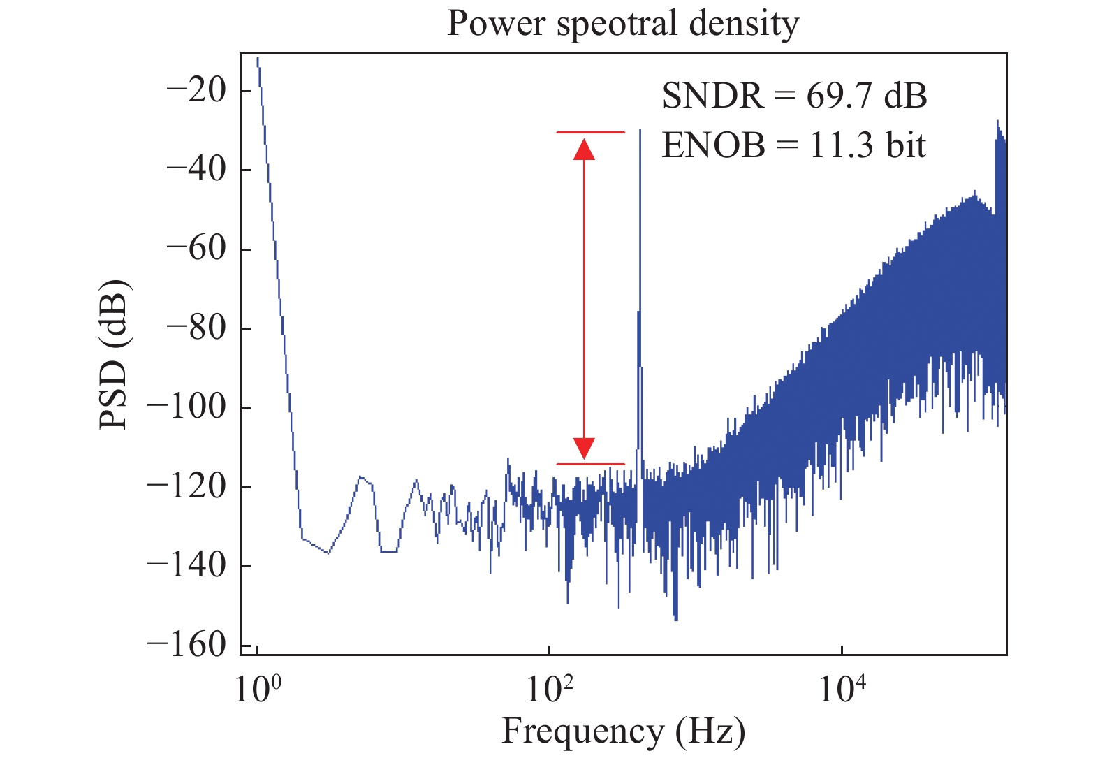
Table 1. Performance comparison.
| Parameter | Ref. [8] | Ref. [9] | Ref. [10] | This work |
| Technology | 130 nm CMOS | 130 nm CMOS | 500 nm CMOS | 130 nm CMOS |
| Power supply (V) | 0.5 | 0.25 | 1.5 | 0.6 |
| Bandwidth (kHz) | 8 | 10 | 0.05 | 0.5 |
| Modulator order | 2 | 2 | 2 | 2 |
| Peak SNDR (dB) | 63.6 | 61 | 55.39 | 69.7 |
| ENOB (bit) | 10.2 | 9.8 | 8.9 | 11.3 |
| Power consumption (μW) | 17 | 7.5 | 58.3 | 5.07 |
| FoM (pJ/conversion step) | 0.9 | 0.41 | 1220 | 2 |
| Area (mm2) | — | 0.37 | 2.25 | 0.72 |
 DownLoad: CSV
| [1] |
Wang Y C, Ke K R, W H Q, et al. A low power low noise analog front end for portable healthcare system. J Semicond, 2015, 36(10): 105008 doi: 10.1088/1674-4926/36/10/105008
|
| [2] |
Mao Y Q, Gao T Q, Xu X D, et al. A fully integrated CMOS super-regenerative wake-up receiver for EEG applications. J Semicond, 2016, 37(9): 095001 doi: 10.1088/1674-4926/37/9/095001
|
| [3] |
Xiao G L, Qin Y L, Xu W L, et al. Demonstration of a fully differential VGA chip with small THD for ECG acquisition system. J Semicond, 2015, 36(10): 105005 doi: 10.1088/1674-4926/36/10/105005
|
| [4] |
Panigrahi A, Parhi A. A 0.5-V body driven pseudo-differential OTA for low voltage and low power applications. IEEE India Conference (INDICON), 2015: 1
|
| [5] |
Zhao X K, Song Z, Chi B Y. A 60-dB DR PGA with DC-offset calibration for short-distance wireless receiver. IEEE International Symposium on VLSI design, Automation and Test (VLSI-DAT), 2015: 1
|
| [6] |
Hsu T F, Huang C P, Chao I J, et al. A first-order low distortion sigma–delta modulator using split DWA technique and SAR quantizer. IEEE International Symposium on VLSI design, Automation and Test (VLSI-DAT), 2015: 13
|
| [7] |
Chae Y, Lee I, Han G. A 0.7-V 36-μW 85dB-DR audio sigma–delta modulator using class-C inverter. IEEE Solid-State Circuits Conference, 2008: 490
|
| [8] |
Abiri E, Pournoori N. A 0.5-V 17 μW second-order delta-sigma modulator based on a self-biased digital inverter in 0.13 μm CMOS. J Basic ad Appl Sci Res, 2012, 2(4): 3476
|
| [9] |
Michel F, Steyaert M. A 250 mV 7.5 μW 61 dB SNDR SC sigma–delta Modulator using near-threshold-voltage-biased inverter amplifier in 130 nm CMOS. IEEE J Solid-State Circuits, 2012, 47(3): 709 doi: 10.1109/JSSC.2011.2179732
|
| [10] |
Yang Y, Yang Y, Lu L, et al. Inverter-based second-order sigma–delta modulator for smart sensor. Electron Lett, 2013, 49(7): 31
|
| [11] |
Chae Y, Han G. Low voltage, low power, inverter-based switch-capacitor delta-sigma modulator. IEEE J Solid-State Circuits, 2009, 44(2): 458 doi: 10.1109/JSSC.2008.2010973
|
| [12] |
Singh A, Rawat V, Agarwal A. Low-power 10-bit 100 MS/s pipelined ADC in digital CMOS technology. IET Circuit, Devices & Systems, 2017, 11(6): 589
|
| [13] |
Xu W G, Gao Y F, Liu X D, et al. A 18 mW 12 bit 50 MS/s SHA-less pipelined ADC. IEEE 12th International Conference on ASIC (ASICON), 2017: 776
|
| [14] |
Chao F B, Chen Y Z, Cao Y F, et al. A proved dither-injection method for memory effect in double sampling pipelined ADC. IEEE 12th International Conference on ASIC (ASICON), 2017: 754
|
| [15] |
Sarma V, Jacob N, Sahoo B, et al. A 250-MHz pipelined ADC-based fs/4 noise-shaping bandpass ADC. IEEE Trans Circuit Syst I, 2017, 99: 1
|
| [16] |
Sehgal R, Goes F V D, Bult K. A 13-mW 64-dB SNDR 280-MS/s pipelined ADC using linearized integrating amplifiers. IEEE J Solid-State Circuits, 2018, 53: 1878 doi: 10.1109/JSSC.2018.2815654
|


Article views: 4939 Times PDF downloads: 102 Times Cited by: 0 Times
Received: 19 April 2018 Revised: 27 June 2018 Online: Accepted Manuscript: 23 July 2018Uncorrected proof: 23 July 2018Published: 13 December 2018
| Citation: |
Chengying Chen, Hongyi Zhang. A 0.6-V, 69-dB subthreshold sigma–delta modulator[J]. Journal of Semiconductors, 2018, 39(12): 125004. doi: 10.1088/1674-4926/39/12/125004
****
C Y Chen, H Y Zhang, A 0.6-V, 69-dB subthreshold sigma–delta modulator[J]. J. Semicond., 2018, 39(12): 125004. doi: 10.1088/1674-4926/39/12/125004.

|
| [1] |
Wang Y C, Ke K R, W H Q, et al. A low power low noise analog front end for portable healthcare system. J Semicond, 2015, 36(10): 105008 doi: 10.1088/1674-4926/36/10/105008
|
| [2] |
Mao Y Q, Gao T Q, Xu X D, et al. A fully integrated CMOS super-regenerative wake-up receiver for EEG applications. J Semicond, 2016, 37(9): 095001 doi: 10.1088/1674-4926/37/9/095001
|
| [3] |
Xiao G L, Qin Y L, Xu W L, et al. Demonstration of a fully differential VGA chip with small THD for ECG acquisition system. J Semicond, 2015, 36(10): 105005 doi: 10.1088/1674-4926/36/10/105005
|
| [4] |
Panigrahi A, Parhi A. A 0.5-V body driven pseudo-differential OTA for low voltage and low power applications. IEEE India Conference (INDICON), 2015: 1
|
| [5] |
Zhao X K, Song Z, Chi B Y. A 60-dB DR PGA with DC-offset calibration for short-distance wireless receiver. IEEE International Symposium on VLSI design, Automation and Test (VLSI-DAT), 2015: 1
|
| [6] |
Hsu T F, Huang C P, Chao I J, et al. A first-order low distortion sigma–delta modulator using split DWA technique and SAR quantizer. IEEE International Symposium on VLSI design, Automation and Test (VLSI-DAT), 2015: 13
|
| [7] |
Chae Y, Lee I, Han G. A 0.7-V 36-μW 85dB-DR audio sigma–delta modulator using class-C inverter. IEEE Solid-State Circuits Conference, 2008: 490
|
| [8] |
Abiri E, Pournoori N. A 0.5-V 17 μW second-order delta-sigma modulator based on a self-biased digital inverter in 0.13 μm CMOS. J Basic ad Appl Sci Res, 2012, 2(4): 3476
|
| [9] |
Michel F, Steyaert M. A 250 mV 7.5 μW 61 dB SNDR SC sigma–delta Modulator using near-threshold-voltage-biased inverter amplifier in 130 nm CMOS. IEEE J Solid-State Circuits, 2012, 47(3): 709 doi: 10.1109/JSSC.2011.2179732
|
| [10] |
Yang Y, Yang Y, Lu L, et al. Inverter-based second-order sigma–delta modulator for smart sensor. Electron Lett, 2013, 49(7): 31
|
| [11] |
Chae Y, Han G. Low voltage, low power, inverter-based switch-capacitor delta-sigma modulator. IEEE J Solid-State Circuits, 2009, 44(2): 458 doi: 10.1109/JSSC.2008.2010973
|
| [12] |
Singh A, Rawat V, Agarwal A. Low-power 10-bit 100 MS/s pipelined ADC in digital CMOS technology. IET Circuit, Devices & Systems, 2017, 11(6): 589
|
| [13] |
Xu W G, Gao Y F, Liu X D, et al. A 18 mW 12 bit 50 MS/s SHA-less pipelined ADC. IEEE 12th International Conference on ASIC (ASICON), 2017: 776
|
| [14] |
Chao F B, Chen Y Z, Cao Y F, et al. A proved dither-injection method for memory effect in double sampling pipelined ADC. IEEE 12th International Conference on ASIC (ASICON), 2017: 754
|
| [15] |
Sarma V, Jacob N, Sahoo B, et al. A 250-MHz pipelined ADC-based fs/4 noise-shaping bandpass ADC. IEEE Trans Circuit Syst I, 2017, 99: 1
|
| [16] |
Sehgal R, Goes F V D, Bult K. A 13-mW 64-dB SNDR 280-MS/s pipelined ADC using linearized integrating amplifiers. IEEE J Solid-State Circuits, 2018, 53: 1878 doi: 10.1109/JSSC.2018.2815654
|

 WeChat ID
Journal of Semiconductors © 2017 All Rights Reserved 京ICP备05085259号-2