| Citation: |
Jiale Su, Xinwei Zhang, Guoping Zhou, Changfeng Xia, Wuqing Zhou, Qing'an Huang. A review: crystalline silicon membranes over sealed cavities for pressure sensors by using silicon migration technology[J]. Journal of Semiconductors, 2018, 39(7): 071005. doi: 10.1088/1674-4926/39/7/071005
****
J L Su, X W Zhang, G P Zhou, C F Xia, W Q Zhou, Q A Huang, A review: crystalline silicon membranes over sealed cavities for pressure sensors by using silicon migration technology[J]. J. Semicond., 2018, 39(7): 071005. doi: 10.1088/1674-4926/39/7/071005.
|
A review: crystalline silicon membranes over sealed cavities for pressure sensors by using silicon migration technology
DOI: 10.1088/1674-4926/39/7/071005
More Information
-
Abstract
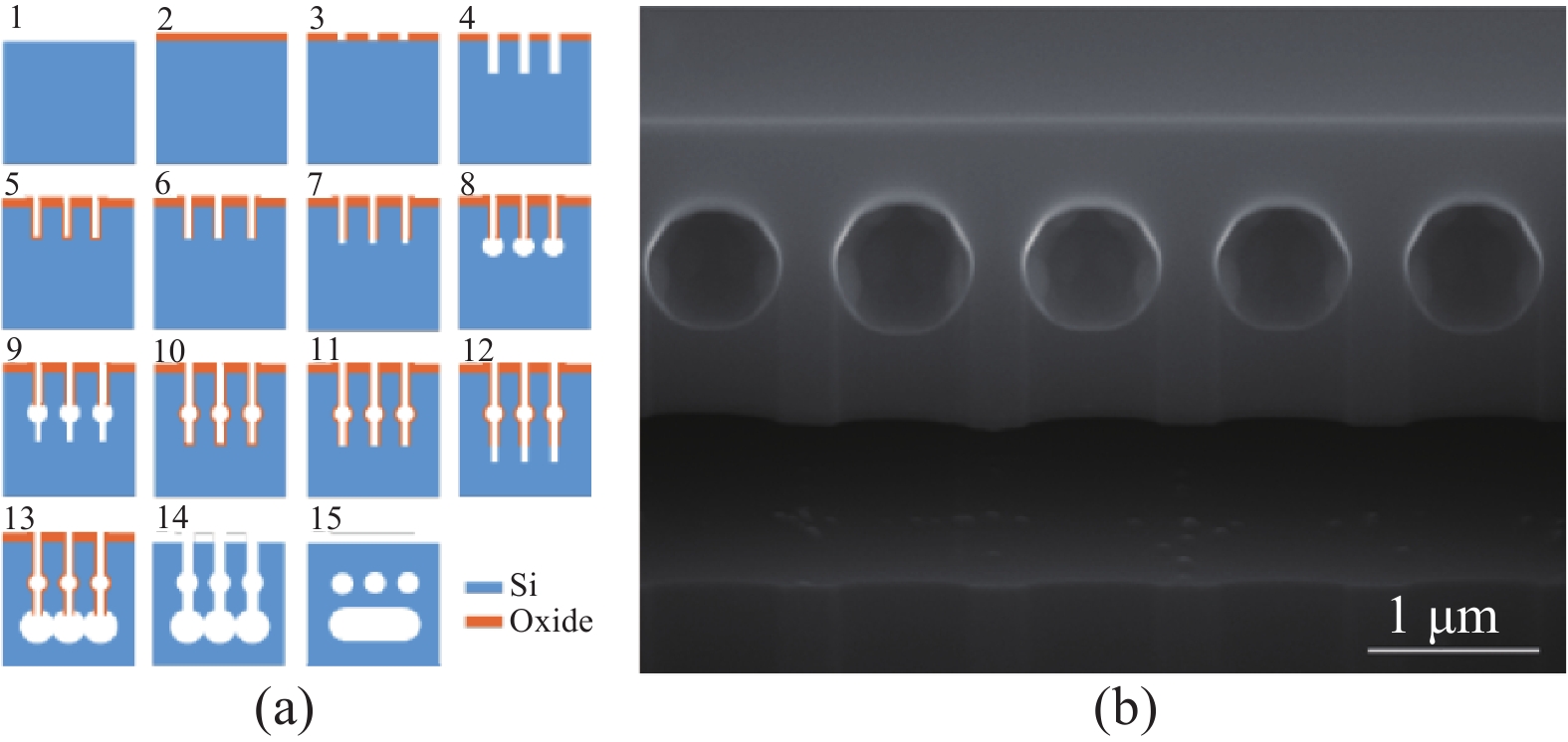
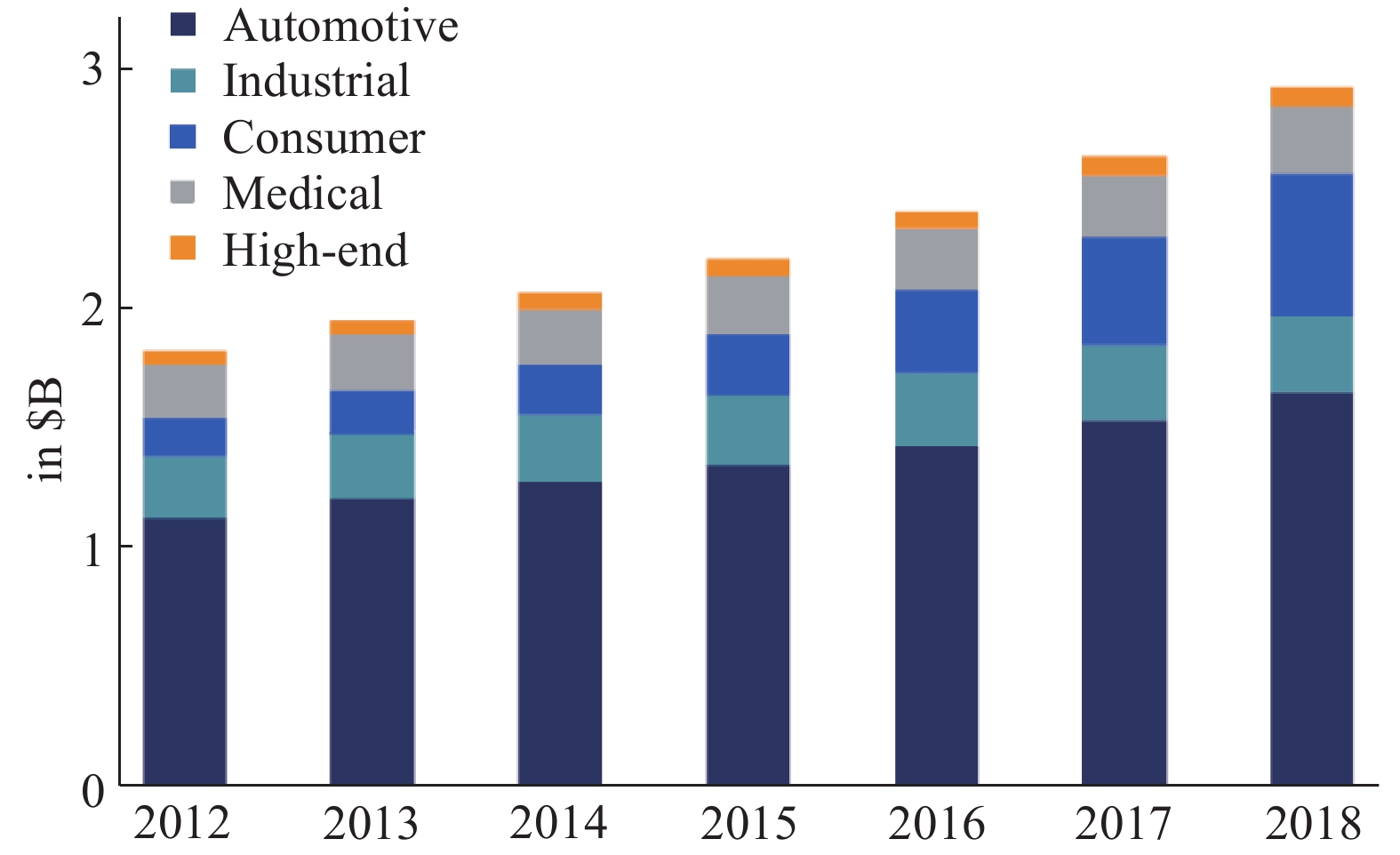
A silicon pressure sensor is one of the very first MEMS components appearing in the microsystem area. The market for the MEMS pressure sensor is rapidly growing due to consumer electronic applications in recent years. Requirements of the pressure sensors with low cost, low power consumption and high accuracy drive one to develop a novel technology. This paper first overviews the historical development of the absolute pressure sensor briefly. It then reviews the state of the art technology for fabricating crystalline silicon membranes over sealed cavities by using the silicon migration technology in detail. By using only one lithographic step, the membranes defined in lateral and vertical dimensions can be realized by the technology. Finally, applications of MEMS through using the silicon migration technology are summarized. -
References
[1] Tufte O N, Chapman P W, Lond D. Silicon diffused element piezoresistive diaphragm. J Appl Phys, 1962, 33(11): 3322 doi: 10.1063/1.1931164[2] Ding W B. Market & Technology report–MEMS pressure sensor. Yole Développement, 2013[3] Wang Z H, Hei Y, Zhu Z M. Preface to the special topic on devices and circuits for wearable and IoT systems. J Semicond, 2017, 38(10): 101001 doi: 10.1088/1674-4926/38/10/101001[4] Barlian A A, Park W T, Mallon J R, et al. Review: semiconductor piezoresistance for microsystems. Proc IEEE, 2009, 97(3): 513 doi: 10.1109/JPROC.2009.2013612[5] Petersen K E. Silicon as a mechanical material. Proc IEEE, 1982, 70(5): 420 doi: 10.1109/PROC.1982.12331[6] Eaton W P, Smith J H. Micromachined pressure sensors: review and recent developments. Smart Mater Struct, 1997, 6(5): 530 doi: 10.1088/0964-1726/6/5/004[7] Esashi M, Sugiyama S, Ikeda K, et al. Vacuum-sealed silicon micromachined pressure sensors. Proc IEEE, 1998, 86(8): 1627 doi: 10.1109/5.704268[8] Schmidt M A. Wafer-to-wafer bonding for microstructure formation. Proc IEEE, 1998, 86(8): 1575 doi: 10.1109/5.704262[9] Renard S. Industrial MEMS on SOI. J Micromechan Microeng, 2000, 10(2): 245 doi: 10.1088/0960-1317/10/2/323[10] Zhao X F, Li D D, Yu Y, et al. Temperature characteristics research of SOI pressure sensor based on asymmetric base region transistor. J Semicond, 2017, 38(7): 074008 doi: 10.1088/1674-4926/38/7/074008[11] Armbruster S, Schafer F, Lammel G, et al. A novel micromachining process for the fabrication of monocrystalline Si-membranes using porous silicon. 12th International Conference on Solid-State Sensors, Actuators and Microsystems, 2003: 246[12] Knese K, Armbruster S, Weber H, Fischer M, Benzel H, and Metz M. Novel technology for capacitive pressure sensors with monocrystalline silicon membranes. 22nd IEEE International Conference on MEMS, 2009: 697[13] Xu G B, Xi Y, Chen X, et al. Application research on the sensitivity of porous silicon. J Semicond, 2017, 38(9): 094003 doi: 10.1088/1674-4926/38/9/094003[14] Wang J C, Li X. Single-side fabricated pressure sensors for IC-foundry-compatible, high-yield, and low-cost volume production. IEEE Electron Device Lett, 2011, 32(7): 979 doi: 10.1109/LED.2011.2147272[15] Jurczak M, Skotnicki T, Paoli M, et al. SON (silicon on nothing) – an innovative process for advanced CMOS. IEEE Trans Electron Devices, 2000, 47(11): 2179 doi: 10.1109/16.877181[16] Sato T, Mitsutake K, Mizushima I, et al. Microstructure transformation of silicon: A newly developed transformation technology for patterning silicon surface using the surface migration of silicon atoms by hydrogen annealing. Jpn J Appl Phys, 2000, 39(9A): 5033 doi: 10.1143/JJAP.39.5033[17] Mizushima I, Sato T, Taniguchi S, et al. Empty-space-in-silicon technique for fabricating a silicon-on-nothing structure. Appl Phys Lett, 2000, 77(20): 3290 doi: 10.1063/1.1324987[18] De Sagazan O, Denoual M, Guil P, et al. Horizontal buried channels in monocristalline silicon, 17th IEEE International Conference on MEMS, 2004: 661[19] Ghannam M Y, Alomar A S, Poortmans J, et al. Interpretation of macropore shape transformation in crystalline silicon upon high temperature processing. J Appl Phys, 2010, 108(7): 074902 doi: 10.1063/1.3462448[20] Sudoh K, Iwasaki H, Kuribayashi H, et al. Numerical study on shape transformation of silicon trenches by high-temperature hydrogen annealing. Jpn J Appl Phys, 2004, 43(9A): 5937 doi: 10.1143/JJAP.43.5937[21] Sudoh K, Iwasaki H, Hiruta R, et al. Void shape evolution and formation of silicon-on-nothing structures during hydrogen annealing of hole arrays on Si (001). J Appl Phys, 2009, 105(8): 083536 doi: 10.1063/1.3116545[22] Sudoh K, Hiruta R, Kuribayashi H. Shape evolution of high aspect ratio holes on Si (001) during hydrogen annealing. J Appl Phys, 2013, 114(18): 183512 doi: 10.1063/1.4829912[23] Sato T, Mizushima I, Taniguchi S, et al. Fabrication of silicon-on-nothing structure by substrate engineering using the empty-space-in-silicon formation technique. Jpn J Appl Phys, 2004, 43(1): 12 doi: 10.1143/JJAP.43.12[24] Depauw V, Gordon I, Beaucarne G. Large-area monocrystalline silicon thin films by annealing of macroporous arrays: understanding and tackling defects in the material. J Appl Phys, 2009, 106(3): 033516 doi: 10.1063/1.3183942[25] Hao X C, Tanaka S, Masuda A, et al. Application of silicon on nothing structure for developing a novel capacitive absolute pressure sensor. IEEE Sens J, 2014, 14(3): 808 doi: 10.1109/JSEN.2013.2288681[26] Zeng F, Wong M. A self-scanned active-matrix tactile sensor realized using silicon-migration technology. J Microelectromechan Syst, 2015, 24(3): 677 doi: 10.1109/JMEMS.2014.2344025[27] Hiruta R, Kuribayashi H, Shimizu R, et al. Flattening of micro-structured Si surfaces by hydrogen annealing. Appl Surf Sci, 2006, 252(15): 5279 doi: 10.1016/j.apsusc.2005.12.051[28] Sudoh K, Nakamura J, Naito M, et al. Formation of silicon-on-nothing structures with extremely flat surfaces. Jpn J Appl Phys, 2013, 52(7): 075601 doi: 10.7567/JJAP.52.075601[29] Bopp M, Coronel P, Bustos J, et al. Silicon nanostructuring for 3D bulk silicon versatile devices. Microelectron Eng, 2009, 86(4–6): 885 doi: 10.1016/j.mee.2008.12.083[30] Wong Y P, Bregman J, Solgaard O. Monolithic silicon-on-nothing photonic crystal pressure sensor. 19th International Conference on Solid-State Sensors, Actuators and Microsystems, 2017: 1963[31] Kim J, Song J, Kim K, et al. Hollow microtube resonators via silicon self-assembly toward subattogram mass sensing applications. Nano Lett, 2016, 16(3): 1537 doi: 10.1021/acs.nanolett.5b03703[32] Park S, Lee Y H, Wi J S, et al. A semitransparent and flexible single crystal Si thin film: silicon on nothing (SON) revisited. ACS Appl Mater Interfaces, 2016, 8(29): 18962 doi: 10.1021/acsami.6b05261[33] Dross F, Baert K, Bearda T, et al. Crystalline thin-foil silicon solar cells: where crystalline quality meets thin-film processing. Progress in Photovoltaics, 2012, 20(6): 770 doi: 10.1002/pip.1238 -
Proportional views


 DownLoad:
