


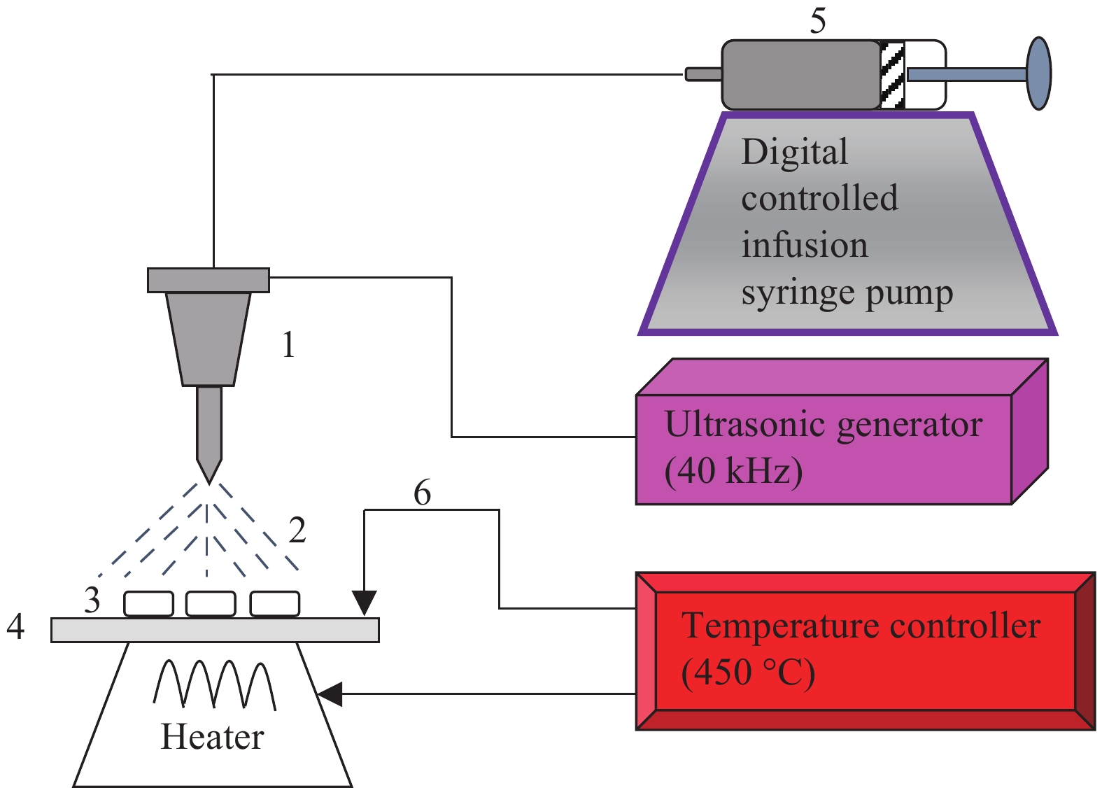
Fig. 1.
(Color online) Experimental set up schematic of the used spray deposition system. 1- Spray nozzle. 2- Droplets stream. 3- Substrate. 4- Substrate holder. 5- Syringe (container of solution). 6- Thermocouple K.
SEMICONDUCTOR MATERIALS
A. Derbali1, H. Saidi1, A. Attaf1, , H. Benamra1, A. Bouhdjer1, N. Attaf2, H. Ezzaouia3, L. Derbali3 and M. S. Aida4
Abstract: The aim of this work is to investigate the dependence of ZnS thin films structural and optical properties with the solution flow rate during the deposition using an ultrasonic spray method. The solution flow rate ranged from 10 to 50 mL/h and the substrate temperature was maintained at 450 °C. The effect of the solution flow rate on the properties of ZnS thin films was investigated by X-ray diffraction (XRD), scanning electron microscopy (SEM), optical transmittance spectroscopy (UV–V) and the four-point method. The X-ray diffraction analysis showed that the deposited material was pure zinc sulphide, it has a cubic sphalerite structure with preferential orientation along the (111) direction. The grain size values were calculated and found to be between 38 to 82 nm. SEM analysis revealed that the deposited thin films have good adherence to the substrate surfaces, are homogeneous and have high density. The average transmission of all films is up more than 65% in the range wavelength from 200 to 1100 nm and their band gap energy values were found between 3.5–3.92 eV. The obtained film thickness varies from 390 to 1040 nm. Moreover, the electric resistivity of the deposited films increases with the increasing of the solution flow rate between 3.51 × 10⁵ and 11 × 105 Ω·cm.
Keywords: zinc sulphide, X-ray diffraction, ultrasonic spray, solution flow rate, optical and electrical properties
| [1] |
Meshram R S, Thombre R M. Structural and optical properties of ZnS thin films deposited by spray pyrolysis technique. International Conference on Benchmarks in Engineering Science and Technology ICBEST, 2012
|
| [2] |
Shinde M S, Ahirrao P B, Patil R S. Structural, optical and electrical properties of nanocrystalline ZnS thin films deposited by novel chemical route. Archives Appl Sci Res, 2011, 3(2): 311
|
| [3] |
Subbaiah Y P V, Prathap P, Ramakrishna Reddy K T. Structural, electrical and optical properties of ZnS films deposited by close-spaced evaporation. Appl Surf Sci, 2006, 253: 2409 doi: 10.1016/j.apsusc.2006.04.063
|
| [4] |
Xue S W, Chen J, Zou C W. Preparation and characterization of cubic lattice ZnS:Na films with (111) preferred orientation. Optoelectron Lett, 2014, 10: 0206 doi: 10.1007/s11801-014-3206-8
|
| [5] |
Ashraf M, Akhtar S M J, Alia Z, et al. The influence of substrate temperature on the structural and optical properties of zns thin films. Semiconductors, 2011, 45: 699 doi: 10.1134/S1063782611050046
|
| [6] |
Liu T Z, Ke H, Zhang H, et al. Effect of four different zinc salts and annealing treatment on growth, structural, mechanical and optical properties of nanocrystalline ZnS thin films by chemical bath deposition. Mater Sci Semicond Process, 2014, 26: 301 doi: 10.1016/j.mssp.2014.05.003
|
| [7] |
Khalifa Z S, Mahmoud S A. Photocatalytic and optical properties of titanium dioxide thin films prepared by metalorganic chemical vapordeposition. Physica E, 2017, 91: 60 doi: 10.1016/j.physe.2017.03.010
|
| [8] |
Zhang L, Szargan R, Chasse T. Electron-diffraction and spectroscopical characterisation of ultrathin ZnS films grown by molecular beamepitaxy on GaP(001). Appl Surf Sci, 2004, 227: 261 doi: 10.1016/j.apsusc.2003.12.002
|
| [9] |
Ku C S, Huang J M, Lin C M, et al. Fabrication of epitaxial ZnO films by atomic-layer deposition with interrupted flow. Thin Solid Films, 2009, 518: 1373 doi: 10.1016/j.tsf.2009.09.018
|
| [10] |
Dimitrova V, Tate J. Synthesis and characterization of some ZnS-based thin film phosphors for electroluminescent device applications. Thin Solid Films, 2000, 365(1): 134 doi: 10.1016/S0040-6090(99)01089-5
|
| [11] |
Kriisa M, Kiirber E, Krunks M, et al. Growth and properties of ZnO films on polymeric substrate by spray pyrolysis method. Thin Solid Films, 2014, 555: 87 doi: 10.1016/j.tsf.2013.05.150
|
| [12] |
Tang W, Cameron D C. Electroluminescent zinc sulphide devices produced by sol–gel processing. Thin Solid Films, 1996, 280: 221 doi: 10.1016/0040-6090(95)08198-4
|
| [13] |
Baranski A S, Fawcett W R, McDonald A C. The mechanism of electrodeposition of cadmium sulphide on inert metals from dimethylsulphoxide solution. Journal of Electroanalytical Chemistry and Interfacial Electrochemistry, 1984, 160: 271 doi: 10.1016/S0022-0728(84)80131-X
|
| [14] |
Dona J M, Herrero J. Chemical bath codeposited CdS/ZnS film characterization. Thin Solid Films, 1995, 5: 268
|
| [15] |
Nabiyouni G, Sahraei R, Toghiany M, et al. preparation and characterization of nanostructured ZnS thin films grown on glass and n-type Si substrates using a new chemical bath deposition technique. Rev Adv Mater Sci, 2011, 27: 52
|
| [16] |
Yoshiyama H, Tanaka S, Mikami I, et al. Role of surface energy in the thin film growth of electroluminescent ZnS, CaS, and SrS. J Cryst Growth, 1988, 86: 56 doi: 10.1016/0022-0248(90)90698-K
|
| [17] |
Kucukomeroglu T, Bacaksiz E, Terzioglu C, et al. Influence of fluorine doping on structural, electrical and optical properties of spray pyrolysis ZnS films. Thin Solid Films, 2008, 516: 2913 doi: 10.1016/j.tsf.2007.05.075
|
| [18] |
Xue S W. Effects of thermal annealing on the optical properties of Ar ion irradiated ZnS films. Ceram Int, 2013, 39(6): 6577 doi: 10.1016/j.ceramint.2013.01.092
|
| [19] |
Jin C, Kim H, Baek K, et al. Effects of coating and thermal annealing on the photoluminescence properties of ZnS/ZnO one-dimensional radial heterostructures. Mater Sci Eng B, 2010, 170: 143 doi: 10.1016/j.mseb.2010.02.029
|
| [20] |
Zhang Z Z, Shen D Z, Zhang J Y, et al. The growth of single cubic phase ZnS thin films on silica glass by plasma-assisted metalorganic chemical vapor deposition. Thin Solid Films, 2006, 513: 114 doi: 10.1016/j.tsf.2006.01.054
|
| [21] |
Subbaiah Y P V, Prathap P, Reddy K T R. Structural, electrical and optical properties of ZnS films deposited by close-spaced evaporation. Appl Surf Sci, 2006, 253: 2409 doi: 10.1016/j.apsusc.2006.04.063
|
| [22] |
Bendjedidi H, Attaf A, Saidi H, et al. Properties of n-type SnO2 semiconductor prepared by spray ultrasonic technique for photovoltaic applications. J Semicond, 2015, 36(12): 123002 doi: 10.1088/1674-4926/36/12/123002
|
| [23] |
Kherchachi I B, Attaf A, Saidi H, et al. Structural, optical and electrical properties of SnxSy thin films grown by spray ultrasonic. J Semicond, 2016, 37(11): 113001 doi: 10.1088/1674-4926/37/11/113001
|
| [24] |
Attaf A, Bouhdjer A, Saidi H, et al. On tuning the preferential crystalline orientation of spray pyrolysis deposited indium oxide thin films. Thin Solid Films, 2017, 625: 177 doi: 10.1016/j.tsf.2017.01.055
|
| [25] |
Kherchachi I B, Saidi H, Attaf A, et al. Influence of solution flow rate on the properties of SnS2 films prepared by ultrasonic spray. Optik, 2016, 127: 4043 doi: 10.1016/j.ijleo.2016.01.120
|
| [26] |
Bouhdjer A, Saidi H, Attafa A, et al. Structural, morphological, optical, and electrical properties of In2O3 nanostructured thin films. Optik, 2016, 127: 7319 doi: 10.1016/j.ijleo.2016.05.035
|
| [27] |
Valenzuela A A, Russer P. High Q coplanar transmission line resonator of YBa2Cu3O7-x on MgO. Appl Phys Lett, 1989, 55: 1029 doi: 10.1063/1.101576
|
| [28] |
Erken O, Gunes M, Ozaslan D, et al. Effect of the deposition time on optical and electrical properties of semiconductor ZnS thin films prepared by chemical bath deposition. Ind J Pure Appl Phys, 2017, 55: 471
|
| [29] |
Gangopadhyay U, Kim K, Dhunge S K, et al. Application of CBD-zinc sulfide film as an antireflection coating on very large area multicrystalline silicon solar cell. Adv Opto-Electrons, 2011, 2007: 1687
|
| [30] |
Sartale S D, Sankapal B R, Lux-Steiner M, et al. Preparation of nanocrystalline ZnS by a new chemical bath deposition route. Thin Solid Films, 2005, 168: 480
|
| [31] |
Antony A, Murali K V, Monoj R, et al. The effect of the pH value on the growth and properties of chemical-bath-deposited ZnS thin films. Mater Chem Phys, 2005, 90: 106 doi: 10.1016/j.matchemphys.2004.10.017
|
| [32] |
Benkhetta Y, Attaf A, Saidi H, et al. Influence of the solution flow rate on the properties of zinc oxide (ZnO) nano-crystalline films synthesized by ultrasonic spray process. Optik, 2016, 127: 3005 doi: 10.1016/j.ijleo.2015.11.236
|
| [33] |
Derbali A, Attafa A, Saidi H, et al. Investigation of structural, optical and electrical properties of ZnS thin films prepared by ultrasonic spray technique for photovoltaic applications. Optik, 2018, 154: 286 doi: 10.1016/j.ijleo.2017.10.034
|
| [34] |
Bouaichia F, Saidi H, Attaf A, et al. The synthesis and characterization of sprayed ZnO thin films: As a function of solution molarity. Main Group Chem, 2016, 15: 57
|
| [35] |
Sahal M, Hartiti B, Mari B, et al. Etude des propriétés physiques des couches minces de ZnO dopées Al, préparées par la méthode de « sol-gel » associée au « spin coating ». Afrique Science, 2006, 02(3): 245
|
| [36] |
Doha M H, Alam M J, Rabeya J, et al. Characterization of chemically deposited ZnS thin films on bare and conducting glass. Optik, 2015, 126: 5194 doi: 10.1016/j.ijleo.2015.09.234
|
| [37] |
Ongul F, Ulutas U, Yuksel S A, et al. Influences of annealing temperature and thickness on ZnS buffer layers for inverted hybrid solar cells. Synth Metals, 2016, 220: 1 doi: 10.1016/j.synthmet.2016.05.017
|
| [38] |
Martínez-Martínez S, Mayen-Hernandez S A, de Moure-Flores F, et al. Sulfiding effects on ZnS thin films obtained by evaporation technique. Vacuum, 2016, 130: 154 doi: 10.1016/j.vacuum.2016.05.011
|
| [39] |
Göde F, Gümüş C, Zor M. Investigations on the physical properties of the polycrystalline ZnS thin films deposited by the chemical bath deposition method. J Cryst Growth, 2200, 7
|
| [40] |
Ates A, Ali Yıldırım M, Kundakcı M, et al. Annealing and light effect on optical and electrical properties of ZnS thin films grown with the SILAR method. Mater Sci Semicond Process, 2007, 10: 281 doi: 10.1016/j.mssp.2008.04.003
|
| [41] |
Ben Achour Z, Ktari T, Ouertani B, et al. Effect of doping level and spray time on zinc oxide thin films produced by spray pyrolysis for transparent electrodes applications. Sens Actuators A, 2007, 134: 447 doi: 10.1016/j.sna.2006.05.001
|
| [42] |
Farid H, Rafea M A, El-Wahidy E F, et al. Preparation and characterization of ZnS nanocrystalline thin films by low cost dip technique. J Mater Sci: Mater Electron, 2014, 25: 2017
|
| [43] |
Goktas A, Aslan F, Yasar E, et al. Preparation and characterisation of thickness dependent nano-structured ZnS thin films by sol-gel technique. J Mater Sci: Mater Electron, 2012, 23: 1361 doi: 10.1007/s10854-011-0599-z
|
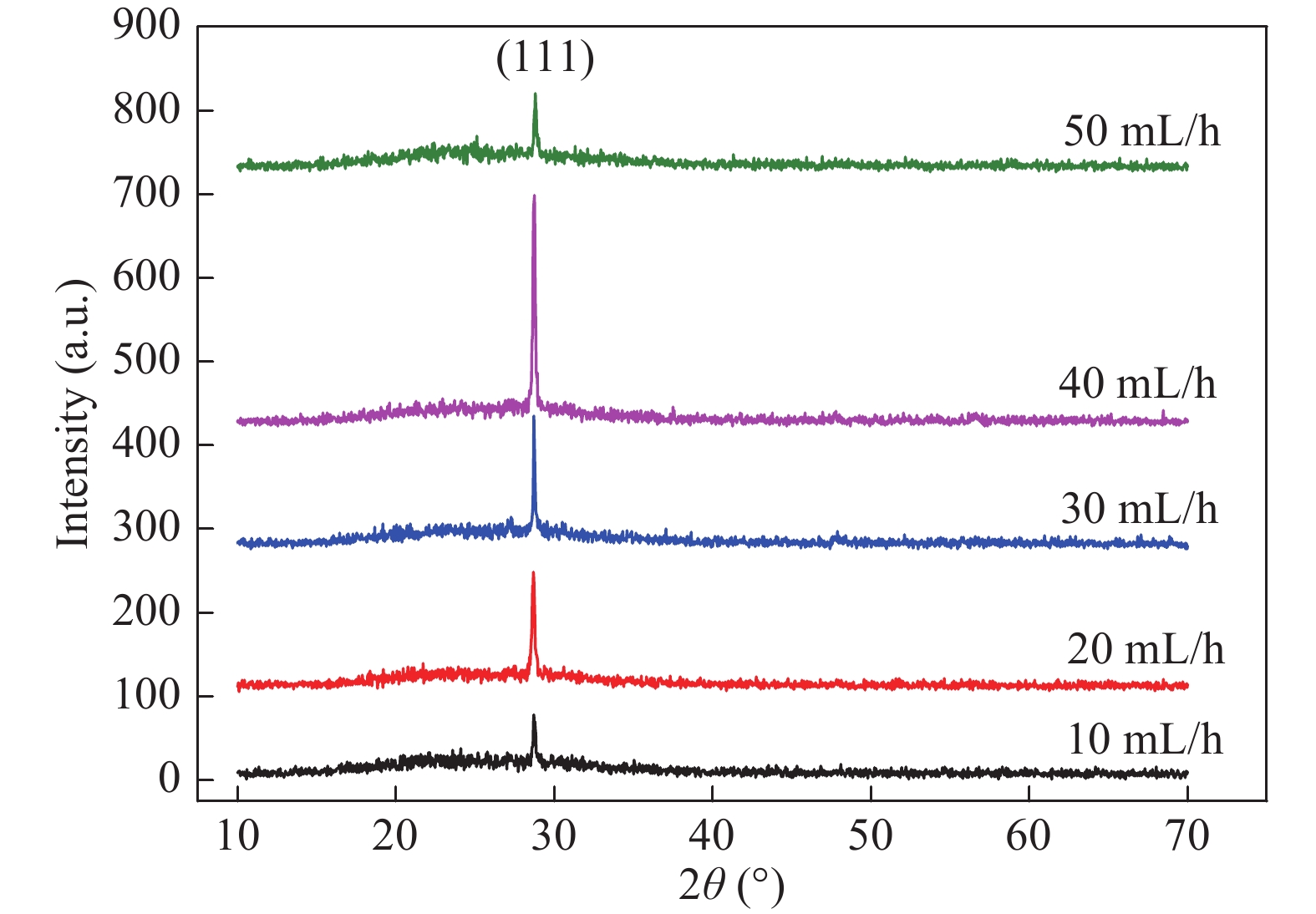
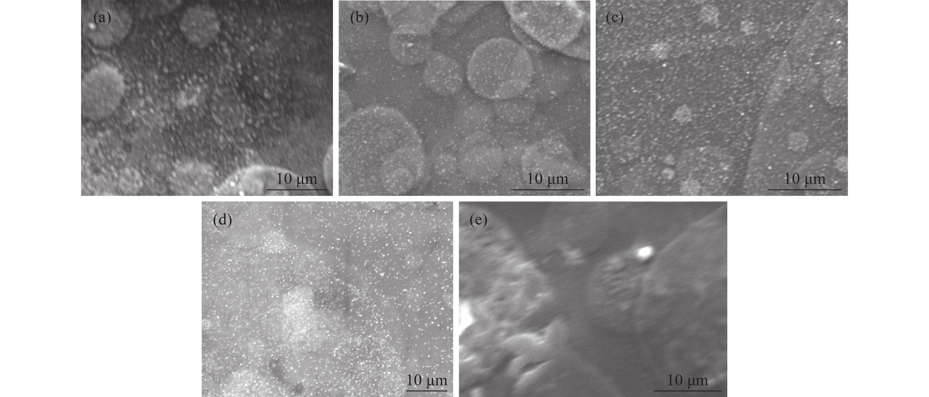
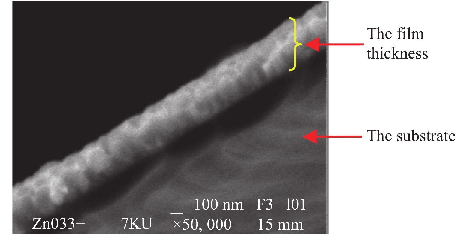
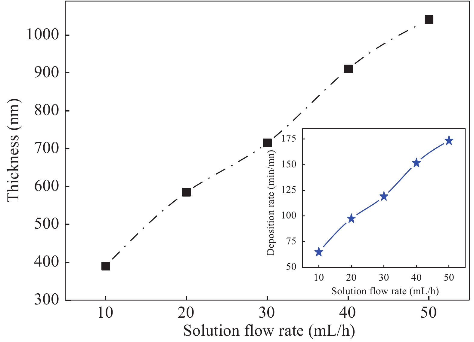
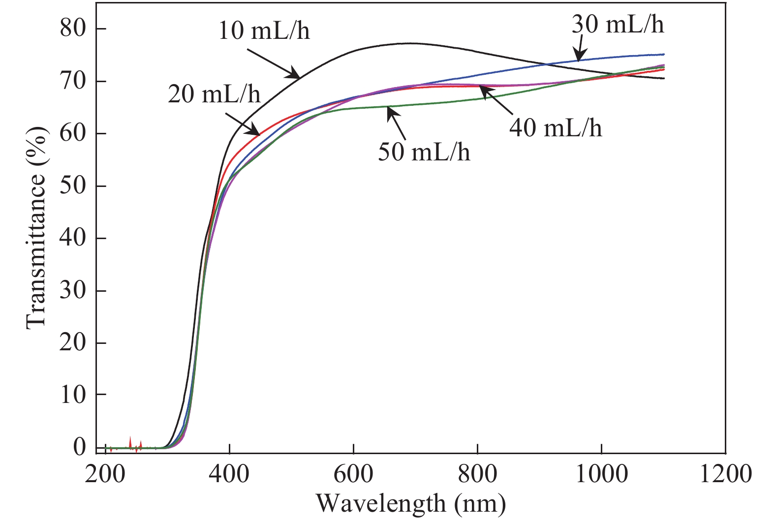
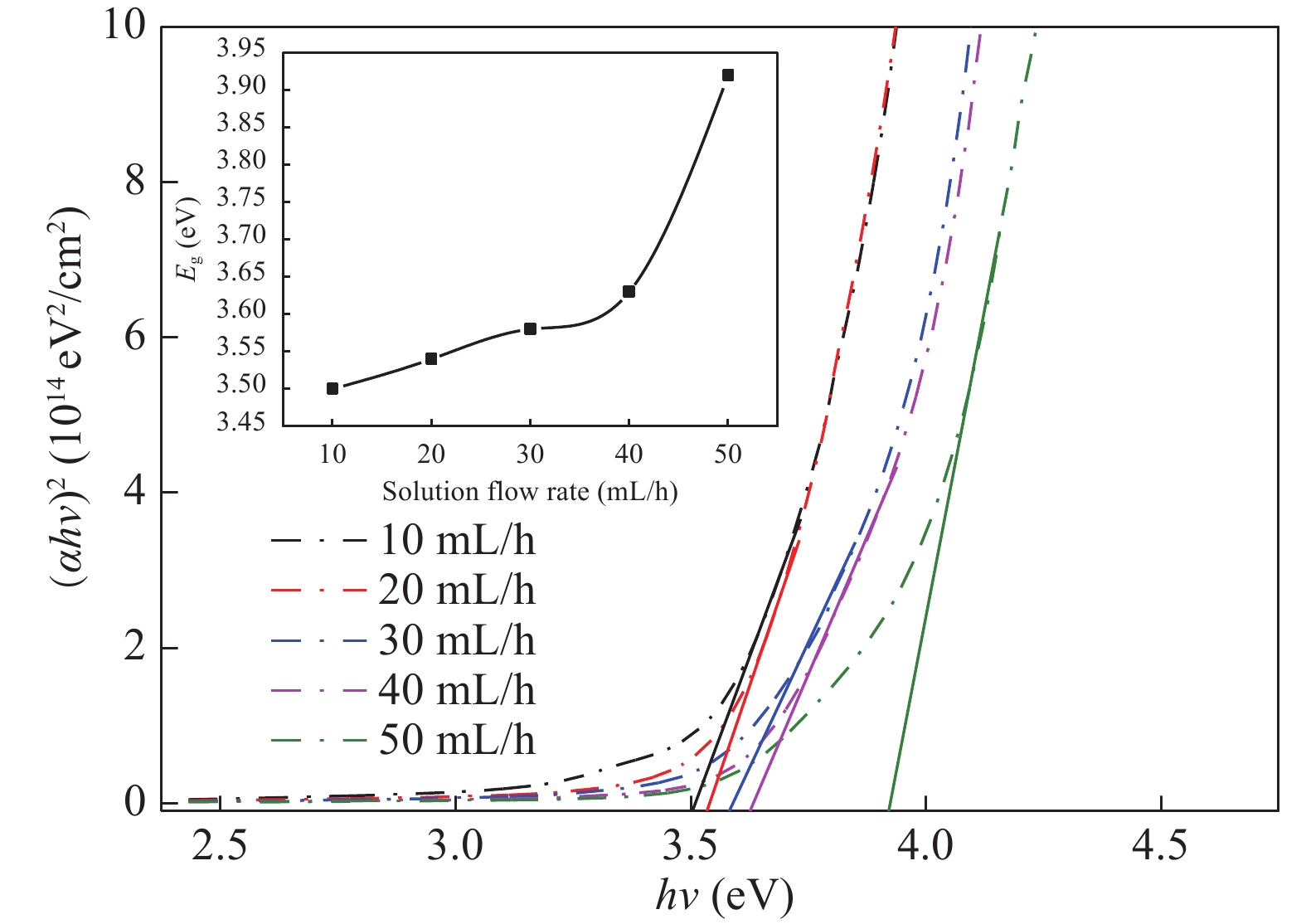
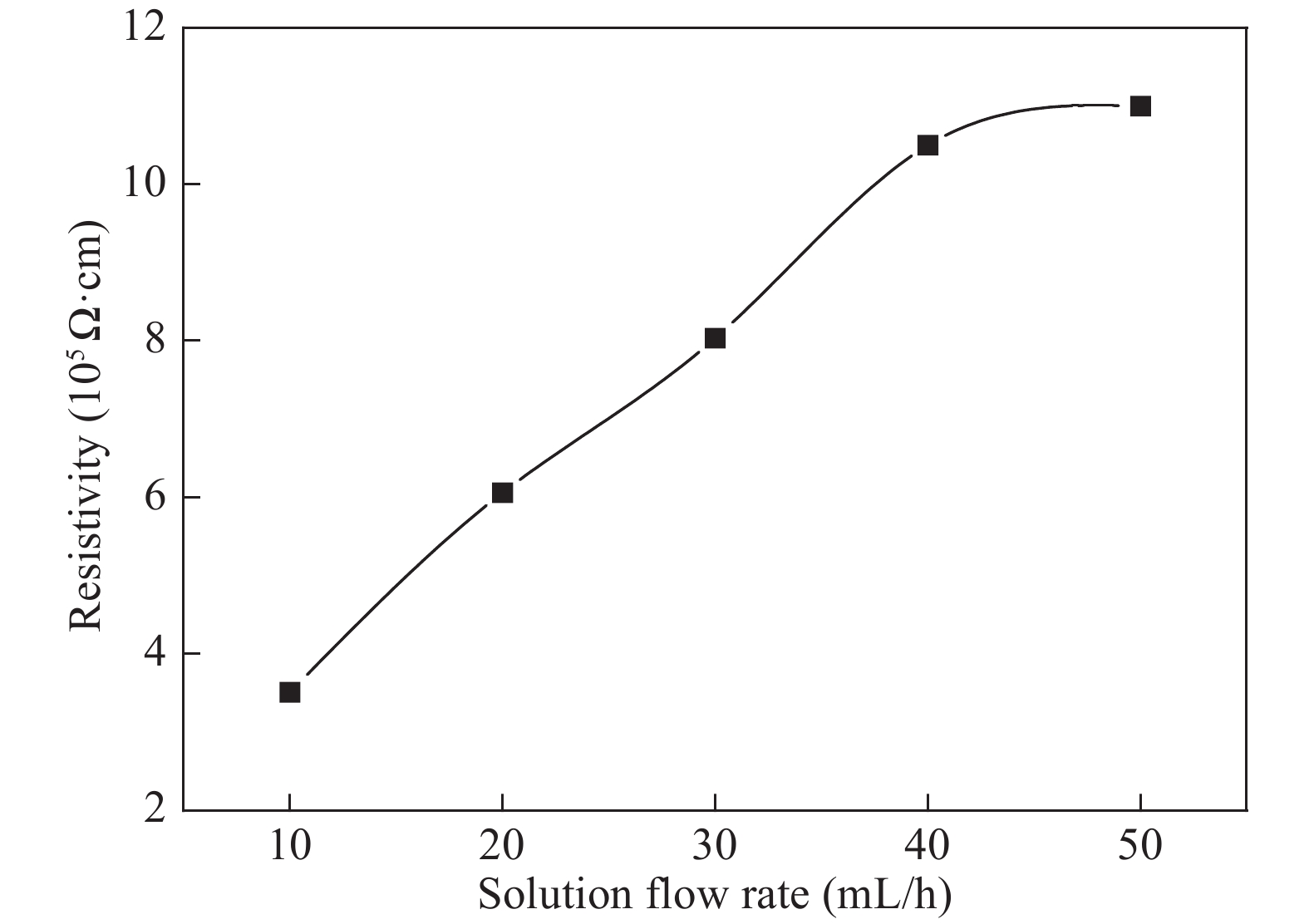
Table 1. Deposition parameters used to prepare the ZnS thin film by spray ultrasonic.
| Deposition parameter | Corresponding value |
| Solution quantity | 30 mL |
| Substrate–nozzle distance | 50 mm |
| Substrate temperature | 450 °C |
| Molarity of solution | 0.1 M |
| Deposition time | 6 min |
| Solution flow rate | 10, 20, 30, 40, 50 mL/h |
 DownLoad: CSV
Table 2. Calculated lattice constant (a) from XRD pattern at different solution flow rates.
| Solution flow rate (mL/h) | hkl planes | 2θ (degree) | Calculated parameters | Reference parameter
(JCPDS card No 05-0566) |
|
| a (Å) | d (Å) | ||||
| 10 | (111) | 28.74 | 5.379 | 3.1055 | a = 5.406 Å, d = 3.123 Å |
| 20 | (111) | 28.68 | 5.383 | 3.108 | |
| 30 | (111) | 28.74 | 5.386 | 3.1095 | |
| 40 | (111) | 28.72 | 5.39 | 3.112 | |
| 50 | (111) | 28.80 | 5.369 | 3.1 | |
DownLoad: CSV
Table 3. Structural parameters of chemically deposited ZnS thin films at different solution flow rates.
| Solution flow rate (mL/h) | (hkl) | 2θ (degree) | FWHM (degree) | D (nm) | δ (1014 lines/m2) | ε (10−4) |
| 10 | (111) | 28.74 | 0.216 | 38 | 6.93 | 9.425 |
| 20 | (111) | 28.68 | 0.144 | 57 | 3.08 | 6.28 |
| 30 | (111) | 28.74 | 0.108 | 76 | 1.73 | 4.71 |
| 40 | (111) | 28.72 | 0.1 | 82 | 1.48 | 4.36 |
| 50 | (111) | 28.80 | 0.2 | 41 | 5.94 | 8.73 |
DownLoad: CSV
| [1] |
Meshram R S, Thombre R M. Structural and optical properties of ZnS thin films deposited by spray pyrolysis technique. International Conference on Benchmarks in Engineering Science and Technology ICBEST, 2012
|
| [2] |
Shinde M S, Ahirrao P B, Patil R S. Structural, optical and electrical properties of nanocrystalline ZnS thin films deposited by novel chemical route. Archives Appl Sci Res, 2011, 3(2): 311
|
| [3] |
Subbaiah Y P V, Prathap P, Ramakrishna Reddy K T. Structural, electrical and optical properties of ZnS films deposited by close-spaced evaporation. Appl Surf Sci, 2006, 253: 2409 doi: 10.1016/j.apsusc.2006.04.063
|
| [4] |
Xue S W, Chen J, Zou C W. Preparation and characterization of cubic lattice ZnS:Na films with (111) preferred orientation. Optoelectron Lett, 2014, 10: 0206 doi: 10.1007/s11801-014-3206-8
|
| [5] |
Ashraf M, Akhtar S M J, Alia Z, et al. The influence of substrate temperature on the structural and optical properties of zns thin films. Semiconductors, 2011, 45: 699 doi: 10.1134/S1063782611050046
|
| [6] |
Liu T Z, Ke H, Zhang H, et al. Effect of four different zinc salts and annealing treatment on growth, structural, mechanical and optical properties of nanocrystalline ZnS thin films by chemical bath deposition. Mater Sci Semicond Process, 2014, 26: 301 doi: 10.1016/j.mssp.2014.05.003
|
| [7] |
Khalifa Z S, Mahmoud S A. Photocatalytic and optical properties of titanium dioxide thin films prepared by metalorganic chemical vapordeposition. Physica E, 2017, 91: 60 doi: 10.1016/j.physe.2017.03.010
|
| [8] |
Zhang L, Szargan R, Chasse T. Electron-diffraction and spectroscopical characterisation of ultrathin ZnS films grown by molecular beamepitaxy on GaP(001). Appl Surf Sci, 2004, 227: 261 doi: 10.1016/j.apsusc.2003.12.002
|
| [9] |
Ku C S, Huang J M, Lin C M, et al. Fabrication of epitaxial ZnO films by atomic-layer deposition with interrupted flow. Thin Solid Films, 2009, 518: 1373 doi: 10.1016/j.tsf.2009.09.018
|
| [10] |
Dimitrova V, Tate J. Synthesis and characterization of some ZnS-based thin film phosphors for electroluminescent device applications. Thin Solid Films, 2000, 365(1): 134 doi: 10.1016/S0040-6090(99)01089-5
|
| [11] |
Kriisa M, Kiirber E, Krunks M, et al. Growth and properties of ZnO films on polymeric substrate by spray pyrolysis method. Thin Solid Films, 2014, 555: 87 doi: 10.1016/j.tsf.2013.05.150
|
| [12] |
Tang W, Cameron D C. Electroluminescent zinc sulphide devices produced by sol–gel processing. Thin Solid Films, 1996, 280: 221 doi: 10.1016/0040-6090(95)08198-4
|
| [13] |
Baranski A S, Fawcett W R, McDonald A C. The mechanism of electrodeposition of cadmium sulphide on inert metals from dimethylsulphoxide solution. Journal of Electroanalytical Chemistry and Interfacial Electrochemistry, 1984, 160: 271 doi: 10.1016/S0022-0728(84)80131-X
|
| [14] |
Dona J M, Herrero J. Chemical bath codeposited CdS/ZnS film characterization. Thin Solid Films, 1995, 5: 268
|
| [15] |
Nabiyouni G, Sahraei R, Toghiany M, et al. preparation and characterization of nanostructured ZnS thin films grown on glass and n-type Si substrates using a new chemical bath deposition technique. Rev Adv Mater Sci, 2011, 27: 52
|
| [16] |
Yoshiyama H, Tanaka S, Mikami I, et al. Role of surface energy in the thin film growth of electroluminescent ZnS, CaS, and SrS. J Cryst Growth, 1988, 86: 56 doi: 10.1016/0022-0248(90)90698-K
|
| [17] |
Kucukomeroglu T, Bacaksiz E, Terzioglu C, et al. Influence of fluorine doping on structural, electrical and optical properties of spray pyrolysis ZnS films. Thin Solid Films, 2008, 516: 2913 doi: 10.1016/j.tsf.2007.05.075
|
| [18] |
Xue S W. Effects of thermal annealing on the optical properties of Ar ion irradiated ZnS films. Ceram Int, 2013, 39(6): 6577 doi: 10.1016/j.ceramint.2013.01.092
|
| [19] |
Jin C, Kim H, Baek K, et al. Effects of coating and thermal annealing on the photoluminescence properties of ZnS/ZnO one-dimensional radial heterostructures. Mater Sci Eng B, 2010, 170: 143 doi: 10.1016/j.mseb.2010.02.029
|
| [20] |
Zhang Z Z, Shen D Z, Zhang J Y, et al. The growth of single cubic phase ZnS thin films on silica glass by plasma-assisted metalorganic chemical vapor deposition. Thin Solid Films, 2006, 513: 114 doi: 10.1016/j.tsf.2006.01.054
|
| [21] |
Subbaiah Y P V, Prathap P, Reddy K T R. Structural, electrical and optical properties of ZnS films deposited by close-spaced evaporation. Appl Surf Sci, 2006, 253: 2409 doi: 10.1016/j.apsusc.2006.04.063
|
| [22] |
Bendjedidi H, Attaf A, Saidi H, et al. Properties of n-type SnO2 semiconductor prepared by spray ultrasonic technique for photovoltaic applications. J Semicond, 2015, 36(12): 123002 doi: 10.1088/1674-4926/36/12/123002
|
| [23] |
Kherchachi I B, Attaf A, Saidi H, et al. Structural, optical and electrical properties of SnxSy thin films grown by spray ultrasonic. J Semicond, 2016, 37(11): 113001 doi: 10.1088/1674-4926/37/11/113001
|
| [24] |
Attaf A, Bouhdjer A, Saidi H, et al. On tuning the preferential crystalline orientation of spray pyrolysis deposited indium oxide thin films. Thin Solid Films, 2017, 625: 177 doi: 10.1016/j.tsf.2017.01.055
|
| [25] |
Kherchachi I B, Saidi H, Attaf A, et al. Influence of solution flow rate on the properties of SnS2 films prepared by ultrasonic spray. Optik, 2016, 127: 4043 doi: 10.1016/j.ijleo.2016.01.120
|
| [26] |
Bouhdjer A, Saidi H, Attafa A, et al. Structural, morphological, optical, and electrical properties of In2O3 nanostructured thin films. Optik, 2016, 127: 7319 doi: 10.1016/j.ijleo.2016.05.035
|
| [27] |
Valenzuela A A, Russer P. High Q coplanar transmission line resonator of YBa2Cu3O7-x on MgO. Appl Phys Lett, 1989, 55: 1029 doi: 10.1063/1.101576
|
| [28] |
Erken O, Gunes M, Ozaslan D, et al. Effect of the deposition time on optical and electrical properties of semiconductor ZnS thin films prepared by chemical bath deposition. Ind J Pure Appl Phys, 2017, 55: 471
|
| [29] |
Gangopadhyay U, Kim K, Dhunge S K, et al. Application of CBD-zinc sulfide film as an antireflection coating on very large area multicrystalline silicon solar cell. Adv Opto-Electrons, 2011, 2007: 1687
|
| [30] |
Sartale S D, Sankapal B R, Lux-Steiner M, et al. Preparation of nanocrystalline ZnS by a new chemical bath deposition route. Thin Solid Films, 2005, 168: 480
|
| [31] |
Antony A, Murali K V, Monoj R, et al. The effect of the pH value on the growth and properties of chemical-bath-deposited ZnS thin films. Mater Chem Phys, 2005, 90: 106 doi: 10.1016/j.matchemphys.2004.10.017
|
| [32] |
Benkhetta Y, Attaf A, Saidi H, et al. Influence of the solution flow rate on the properties of zinc oxide (ZnO) nano-crystalline films synthesized by ultrasonic spray process. Optik, 2016, 127: 3005 doi: 10.1016/j.ijleo.2015.11.236
|
| [33] |
Derbali A, Attafa A, Saidi H, et al. Investigation of structural, optical and electrical properties of ZnS thin films prepared by ultrasonic spray technique for photovoltaic applications. Optik, 2018, 154: 286 doi: 10.1016/j.ijleo.2017.10.034
|
| [34] |
Bouaichia F, Saidi H, Attaf A, et al. The synthesis and characterization of sprayed ZnO thin films: As a function of solution molarity. Main Group Chem, 2016, 15: 57
|
| [35] |
Sahal M, Hartiti B, Mari B, et al. Etude des propriétés physiques des couches minces de ZnO dopées Al, préparées par la méthode de « sol-gel » associée au « spin coating ». Afrique Science, 2006, 02(3): 245
|
| [36] |
Doha M H, Alam M J, Rabeya J, et al. Characterization of chemically deposited ZnS thin films on bare and conducting glass. Optik, 2015, 126: 5194 doi: 10.1016/j.ijleo.2015.09.234
|
| [37] |
Ongul F, Ulutas U, Yuksel S A, et al. Influences of annealing temperature and thickness on ZnS buffer layers for inverted hybrid solar cells. Synth Metals, 2016, 220: 1 doi: 10.1016/j.synthmet.2016.05.017
|
| [38] |
Martínez-Martínez S, Mayen-Hernandez S A, de Moure-Flores F, et al. Sulfiding effects on ZnS thin films obtained by evaporation technique. Vacuum, 2016, 130: 154 doi: 10.1016/j.vacuum.2016.05.011
|
| [39] |
Göde F, Gümüş C, Zor M. Investigations on the physical properties of the polycrystalline ZnS thin films deposited by the chemical bath deposition method. J Cryst Growth, 2200, 7
|
| [40] |
Ates A, Ali Yıldırım M, Kundakcı M, et al. Annealing and light effect on optical and electrical properties of ZnS thin films grown with the SILAR method. Mater Sci Semicond Process, 2007, 10: 281 doi: 10.1016/j.mssp.2008.04.003
|
| [41] |
Ben Achour Z, Ktari T, Ouertani B, et al. Effect of doping level and spray time on zinc oxide thin films produced by spray pyrolysis for transparent electrodes applications. Sens Actuators A, 2007, 134: 447 doi: 10.1016/j.sna.2006.05.001
|
| [42] |
Farid H, Rafea M A, El-Wahidy E F, et al. Preparation and characterization of ZnS nanocrystalline thin films by low cost dip technique. J Mater Sci: Mater Electron, 2014, 25: 2017
|
| [43] |
Goktas A, Aslan F, Yasar E, et al. Preparation and characterisation of thickness dependent nano-structured ZnS thin films by sol-gel technique. J Mater Sci: Mater Electron, 2012, 23: 1361 doi: 10.1007/s10854-011-0599-z
|


Article views: 5225 Times PDF downloads: 169 Times Cited by: 0 Times
Received: 09 December 2017 Revised: 14 February 2018 Online: Uncorrected proof: 16 May 2018Accepted Manuscript: 05 July 2018Published: 01 September 2018
| Citation: |
A. Derbali, H. Saidi, A. Attaf, H. Benamra, A. Bouhdjer, N. Attaf, H. Ezzaouia, L. Derbali, M. S. Aida. Solution flow rate influence on ZnS thin films properties grown by ultrasonic spray for optoelectronic application[J]. Journal of Semiconductors, 2018, 39(9): 093001. doi: 10.1088/1674-4926/39/9/093001
****
A Derbali, H Saidi, A Attaf, H Benamra, A Bouhdjer, N Attaf, H Ezzaouia, L Derbali, M S Aida, Solution flow rate influence on ZnS thin films properties grown by ultrasonic spray for optoelectronic application[J]. J. Semicond., 2018, 39(9): 093001. doi: 10.1088/1674-4926/39/9/093001.

|
| [1] |
Meshram R S, Thombre R M. Structural and optical properties of ZnS thin films deposited by spray pyrolysis technique. International Conference on Benchmarks in Engineering Science and Technology ICBEST, 2012
|
| [2] |
Shinde M S, Ahirrao P B, Patil R S. Structural, optical and electrical properties of nanocrystalline ZnS thin films deposited by novel chemical route. Archives Appl Sci Res, 2011, 3(2): 311
|
| [3] |
Subbaiah Y P V, Prathap P, Ramakrishna Reddy K T. Structural, electrical and optical properties of ZnS films deposited by close-spaced evaporation. Appl Surf Sci, 2006, 253: 2409 doi: 10.1016/j.apsusc.2006.04.063
|
| [4] |
Xue S W, Chen J, Zou C W. Preparation and characterization of cubic lattice ZnS:Na films with (111) preferred orientation. Optoelectron Lett, 2014, 10: 0206 doi: 10.1007/s11801-014-3206-8
|
| [5] |
Ashraf M, Akhtar S M J, Alia Z, et al. The influence of substrate temperature on the structural and optical properties of zns thin films. Semiconductors, 2011, 45: 699 doi: 10.1134/S1063782611050046
|
| [6] |
Liu T Z, Ke H, Zhang H, et al. Effect of four different zinc salts and annealing treatment on growth, structural, mechanical and optical properties of nanocrystalline ZnS thin films by chemical bath deposition. Mater Sci Semicond Process, 2014, 26: 301 doi: 10.1016/j.mssp.2014.05.003
|
| [7] |
Khalifa Z S, Mahmoud S A. Photocatalytic and optical properties of titanium dioxide thin films prepared by metalorganic chemical vapordeposition. Physica E, 2017, 91: 60 doi: 10.1016/j.physe.2017.03.010
|
| [8] |
Zhang L, Szargan R, Chasse T. Electron-diffraction and spectroscopical characterisation of ultrathin ZnS films grown by molecular beamepitaxy on GaP(001). Appl Surf Sci, 2004, 227: 261 doi: 10.1016/j.apsusc.2003.12.002
|
| [9] |
Ku C S, Huang J M, Lin C M, et al. Fabrication of epitaxial ZnO films by atomic-layer deposition with interrupted flow. Thin Solid Films, 2009, 518: 1373 doi: 10.1016/j.tsf.2009.09.018
|
| [10] |
Dimitrova V, Tate J. Synthesis and characterization of some ZnS-based thin film phosphors for electroluminescent device applications. Thin Solid Films, 2000, 365(1): 134 doi: 10.1016/S0040-6090(99)01089-5
|
| [11] |
Kriisa M, Kiirber E, Krunks M, et al. Growth and properties of ZnO films on polymeric substrate by spray pyrolysis method. Thin Solid Films, 2014, 555: 87 doi: 10.1016/j.tsf.2013.05.150
|
| [12] |
Tang W, Cameron D C. Electroluminescent zinc sulphide devices produced by sol–gel processing. Thin Solid Films, 1996, 280: 221 doi: 10.1016/0040-6090(95)08198-4
|
| [13] |
Baranski A S, Fawcett W R, McDonald A C. The mechanism of electrodeposition of cadmium sulphide on inert metals from dimethylsulphoxide solution. Journal of Electroanalytical Chemistry and Interfacial Electrochemistry, 1984, 160: 271 doi: 10.1016/S0022-0728(84)80131-X
|
| [14] |
Dona J M, Herrero J. Chemical bath codeposited CdS/ZnS film characterization. Thin Solid Films, 1995, 5: 268
|
| [15] |
Nabiyouni G, Sahraei R, Toghiany M, et al. preparation and characterization of nanostructured ZnS thin films grown on glass and n-type Si substrates using a new chemical bath deposition technique. Rev Adv Mater Sci, 2011, 27: 52
|
| [16] |
Yoshiyama H, Tanaka S, Mikami I, et al. Role of surface energy in the thin film growth of electroluminescent ZnS, CaS, and SrS. J Cryst Growth, 1988, 86: 56 doi: 10.1016/0022-0248(90)90698-K
|
| [17] |
Kucukomeroglu T, Bacaksiz E, Terzioglu C, et al. Influence of fluorine doping on structural, electrical and optical properties of spray pyrolysis ZnS films. Thin Solid Films, 2008, 516: 2913 doi: 10.1016/j.tsf.2007.05.075
|
| [18] |
Xue S W. Effects of thermal annealing on the optical properties of Ar ion irradiated ZnS films. Ceram Int, 2013, 39(6): 6577 doi: 10.1016/j.ceramint.2013.01.092
|
| [19] |
Jin C, Kim H, Baek K, et al. Effects of coating and thermal annealing on the photoluminescence properties of ZnS/ZnO one-dimensional radial heterostructures. Mater Sci Eng B, 2010, 170: 143 doi: 10.1016/j.mseb.2010.02.029
|
| [20] |
Zhang Z Z, Shen D Z, Zhang J Y, et al. The growth of single cubic phase ZnS thin films on silica glass by plasma-assisted metalorganic chemical vapor deposition. Thin Solid Films, 2006, 513: 114 doi: 10.1016/j.tsf.2006.01.054
|
| [21] |
Subbaiah Y P V, Prathap P, Reddy K T R. Structural, electrical and optical properties of ZnS films deposited by close-spaced evaporation. Appl Surf Sci, 2006, 253: 2409 doi: 10.1016/j.apsusc.2006.04.063
|
| [22] |
Bendjedidi H, Attaf A, Saidi H, et al. Properties of n-type SnO2 semiconductor prepared by spray ultrasonic technique for photovoltaic applications. J Semicond, 2015, 36(12): 123002 doi: 10.1088/1674-4926/36/12/123002
|
| [23] |
Kherchachi I B, Attaf A, Saidi H, et al. Structural, optical and electrical properties of SnxSy thin films grown by spray ultrasonic. J Semicond, 2016, 37(11): 113001 doi: 10.1088/1674-4926/37/11/113001
|
| [24] |
Attaf A, Bouhdjer A, Saidi H, et al. On tuning the preferential crystalline orientation of spray pyrolysis deposited indium oxide thin films. Thin Solid Films, 2017, 625: 177 doi: 10.1016/j.tsf.2017.01.055
|
| [25] |
Kherchachi I B, Saidi H, Attaf A, et al. Influence of solution flow rate on the properties of SnS2 films prepared by ultrasonic spray. Optik, 2016, 127: 4043 doi: 10.1016/j.ijleo.2016.01.120
|
| [26] |
Bouhdjer A, Saidi H, Attafa A, et al. Structural, morphological, optical, and electrical properties of In2O3 nanostructured thin films. Optik, 2016, 127: 7319 doi: 10.1016/j.ijleo.2016.05.035
|
| [27] |
Valenzuela A A, Russer P. High Q coplanar transmission line resonator of YBa2Cu3O7-x on MgO. Appl Phys Lett, 1989, 55: 1029 doi: 10.1063/1.101576
|
| [28] |
Erken O, Gunes M, Ozaslan D, et al. Effect of the deposition time on optical and electrical properties of semiconductor ZnS thin films prepared by chemical bath deposition. Ind J Pure Appl Phys, 2017, 55: 471
|
| [29] |
Gangopadhyay U, Kim K, Dhunge S K, et al. Application of CBD-zinc sulfide film as an antireflection coating on very large area multicrystalline silicon solar cell. Adv Opto-Electrons, 2011, 2007: 1687
|
| [30] |
Sartale S D, Sankapal B R, Lux-Steiner M, et al. Preparation of nanocrystalline ZnS by a new chemical bath deposition route. Thin Solid Films, 2005, 168: 480
|
| [31] |
Antony A, Murali K V, Monoj R, et al. The effect of the pH value on the growth and properties of chemical-bath-deposited ZnS thin films. Mater Chem Phys, 2005, 90: 106 doi: 10.1016/j.matchemphys.2004.10.017
|
| [32] |
Benkhetta Y, Attaf A, Saidi H, et al. Influence of the solution flow rate on the properties of zinc oxide (ZnO) nano-crystalline films synthesized by ultrasonic spray process. Optik, 2016, 127: 3005 doi: 10.1016/j.ijleo.2015.11.236
|
| [33] |
Derbali A, Attafa A, Saidi H, et al. Investigation of structural, optical and electrical properties of ZnS thin films prepared by ultrasonic spray technique for photovoltaic applications. Optik, 2018, 154: 286 doi: 10.1016/j.ijleo.2017.10.034
|
| [34] |
Bouaichia F, Saidi H, Attaf A, et al. The synthesis and characterization of sprayed ZnO thin films: As a function of solution molarity. Main Group Chem, 2016, 15: 57
|
| [35] |
Sahal M, Hartiti B, Mari B, et al. Etude des propriétés physiques des couches minces de ZnO dopées Al, préparées par la méthode de « sol-gel » associée au « spin coating ». Afrique Science, 2006, 02(3): 245
|
| [36] |
Doha M H, Alam M J, Rabeya J, et al. Characterization of chemically deposited ZnS thin films on bare and conducting glass. Optik, 2015, 126: 5194 doi: 10.1016/j.ijleo.2015.09.234
|
| [37] |
Ongul F, Ulutas U, Yuksel S A, et al. Influences of annealing temperature and thickness on ZnS buffer layers for inverted hybrid solar cells. Synth Metals, 2016, 220: 1 doi: 10.1016/j.synthmet.2016.05.017
|
| [38] |
Martínez-Martínez S, Mayen-Hernandez S A, de Moure-Flores F, et al. Sulfiding effects on ZnS thin films obtained by evaporation technique. Vacuum, 2016, 130: 154 doi: 10.1016/j.vacuum.2016.05.011
|
| [39] |
Göde F, Gümüş C, Zor M. Investigations on the physical properties of the polycrystalline ZnS thin films deposited by the chemical bath deposition method. J Cryst Growth, 2200, 7
|
| [40] |
Ates A, Ali Yıldırım M, Kundakcı M, et al. Annealing and light effect on optical and electrical properties of ZnS thin films grown with the SILAR method. Mater Sci Semicond Process, 2007, 10: 281 doi: 10.1016/j.mssp.2008.04.003
|
| [41] |
Ben Achour Z, Ktari T, Ouertani B, et al. Effect of doping level and spray time on zinc oxide thin films produced by spray pyrolysis for transparent electrodes applications. Sens Actuators A, 2007, 134: 447 doi: 10.1016/j.sna.2006.05.001
|
| [42] |
Farid H, Rafea M A, El-Wahidy E F, et al. Preparation and characterization of ZnS nanocrystalline thin films by low cost dip technique. J Mater Sci: Mater Electron, 2014, 25: 2017
|
| [43] |
Goktas A, Aslan F, Yasar E, et al. Preparation and characterisation of thickness dependent nano-structured ZnS thin films by sol-gel technique. J Mater Sci: Mater Electron, 2012, 23: 1361 doi: 10.1007/s10854-011-0599-z
|

 WeChat ID
Journal of Semiconductors © 2017 All Rights Reserved 京ICP备05085259号-2


