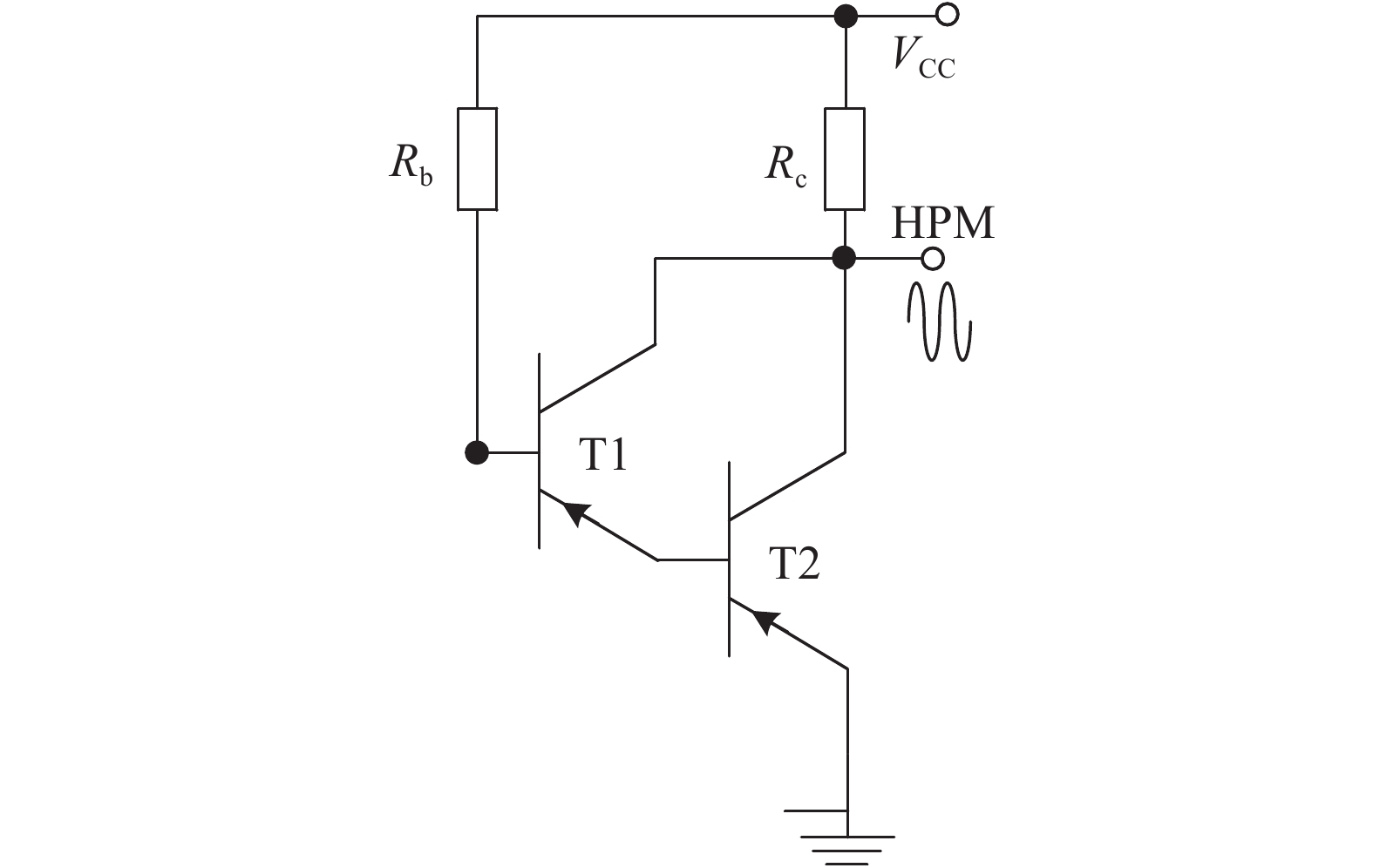
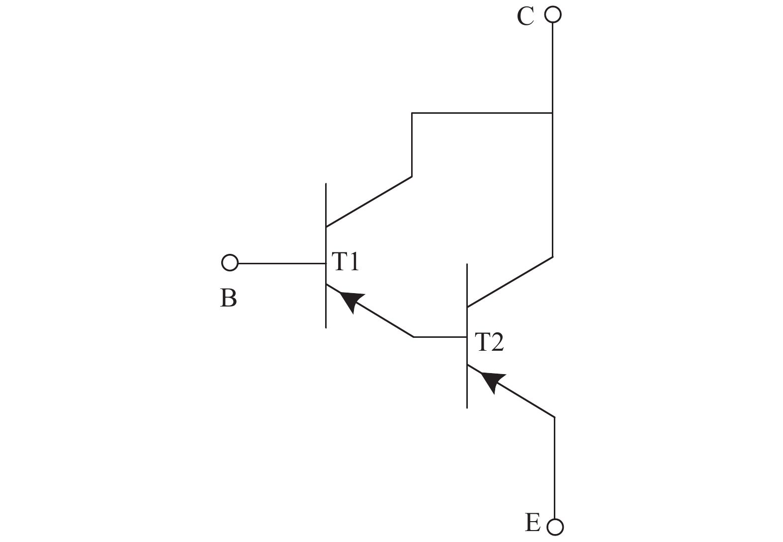
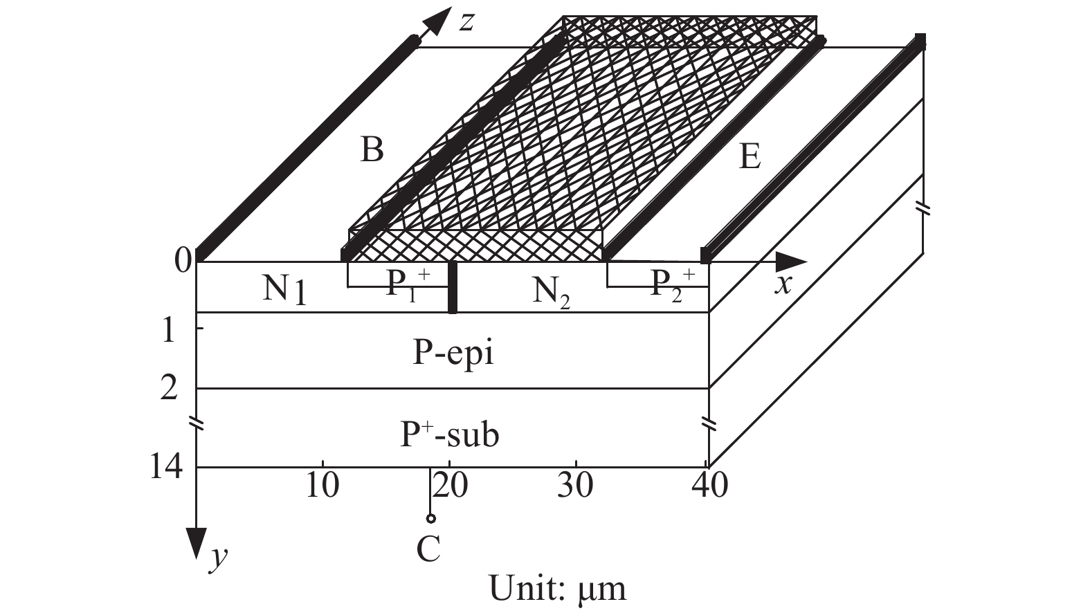
Processing math: 100%
J. Semicond. > 2018, Volume 39 > Issue 9 > 094005

SEMICONDUCTOR DEVICES

The influence of pulsed parameters on the damage of a Darlington transistor

Qiankun Wang, Changchun Chai, Yuqian Liu and Yintang Yang

+ Author Affiliations

 Corresponding author: Qiankun Wang, Email: wang__qk@163.com

DOI: 10.1088/1674-4926/39/9/094005

PDF

Turn off MathJax

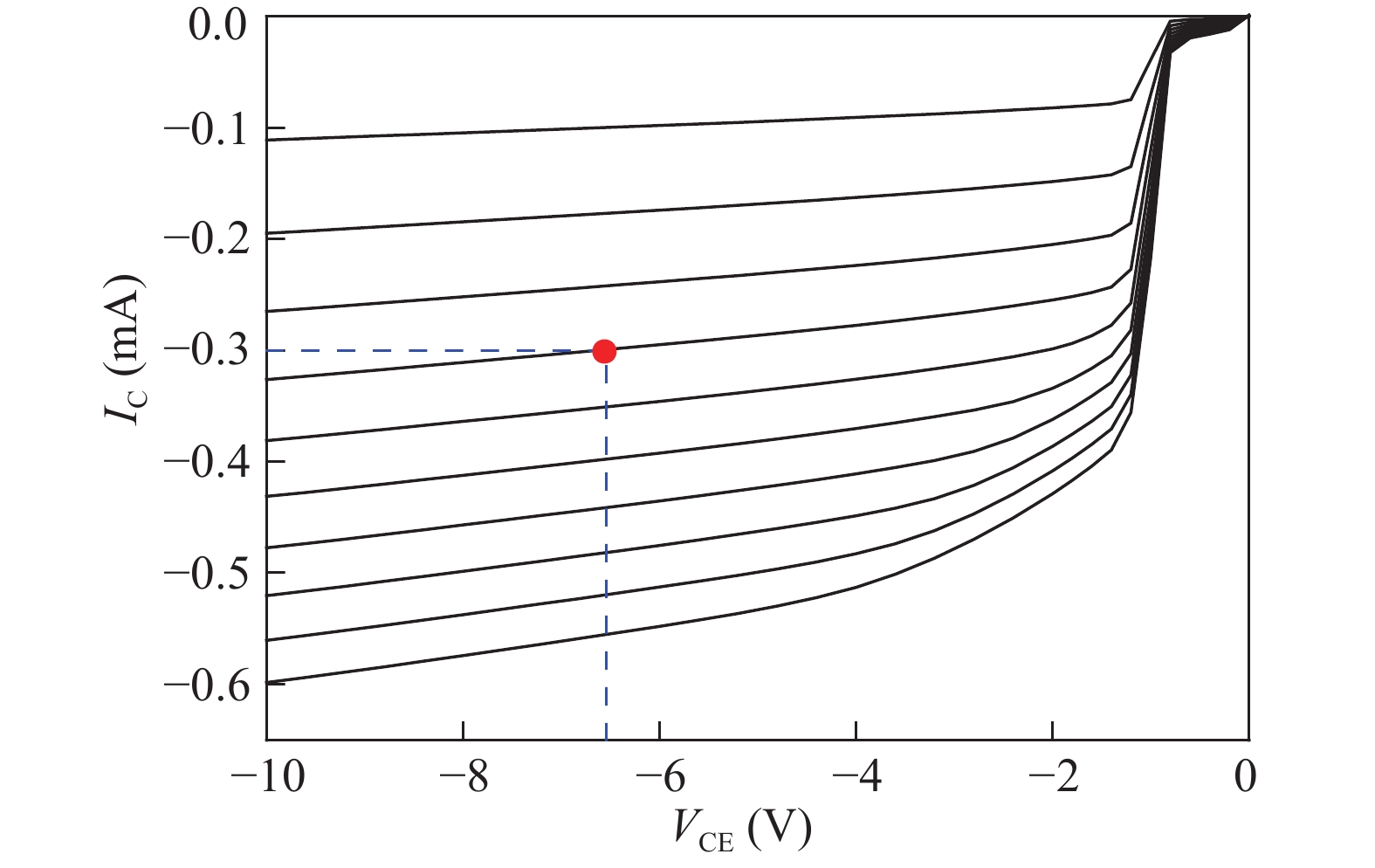
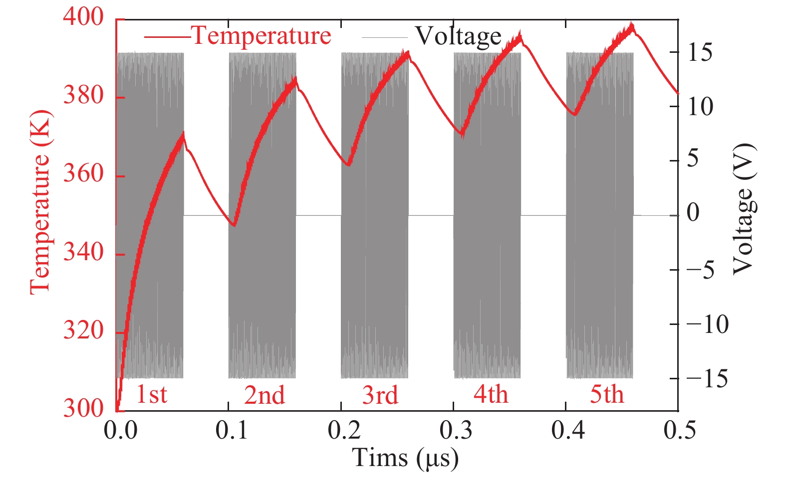
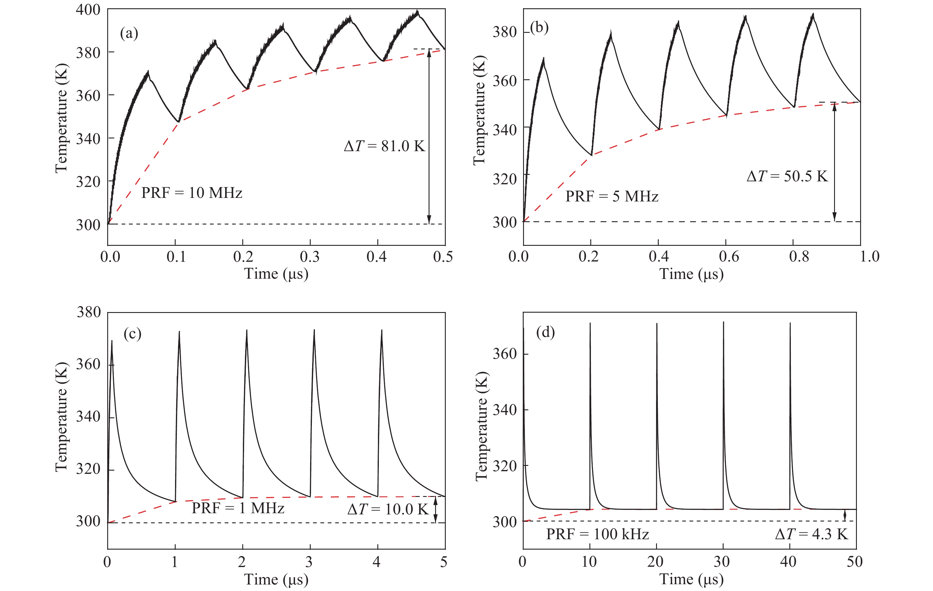
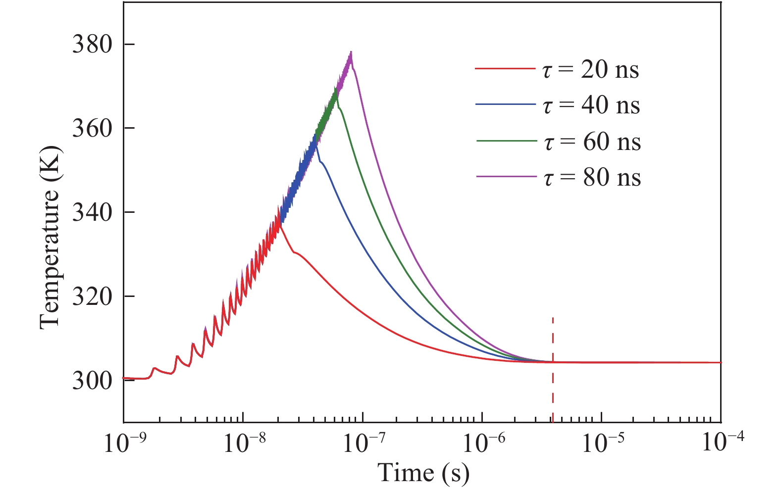
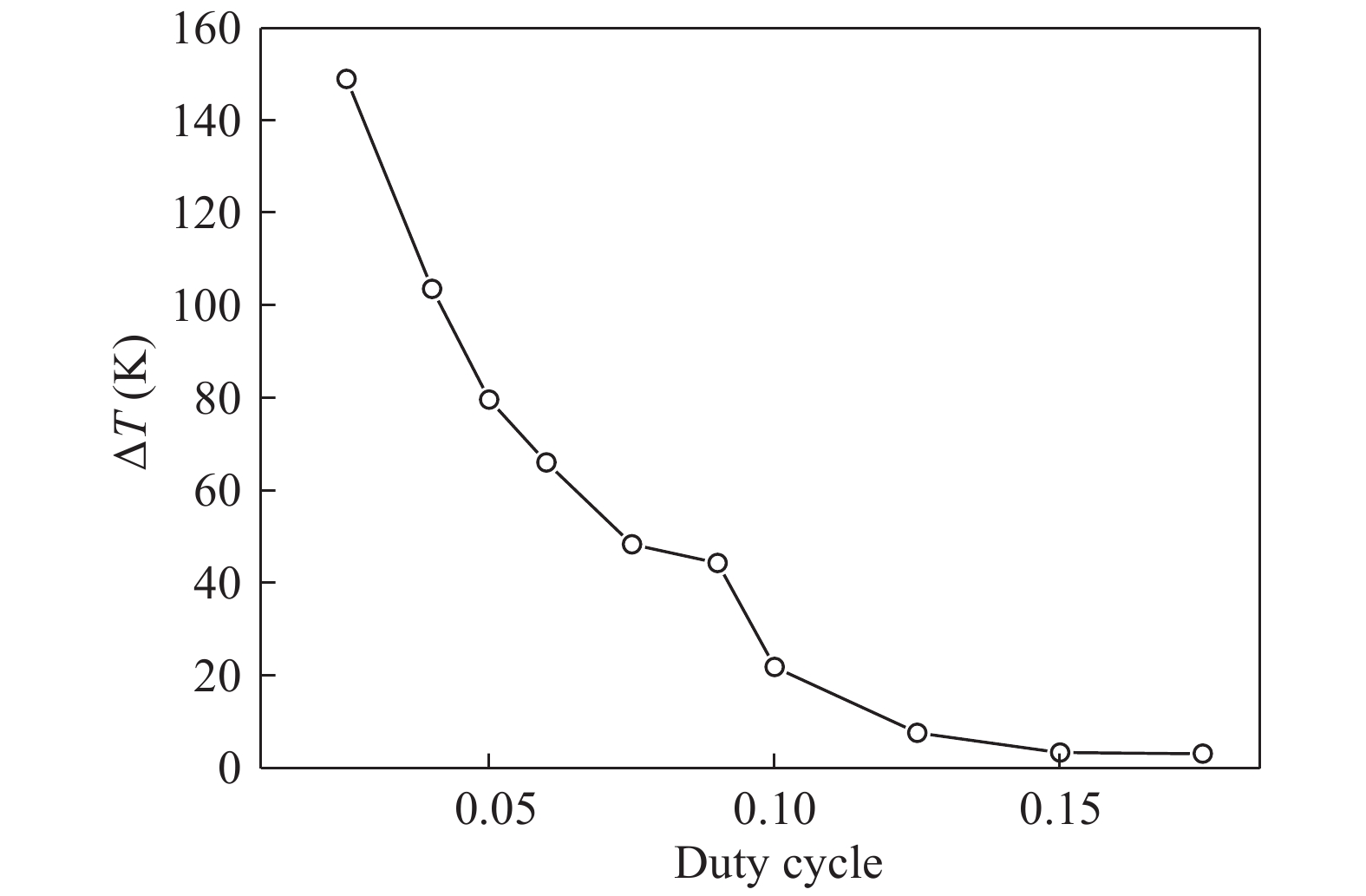
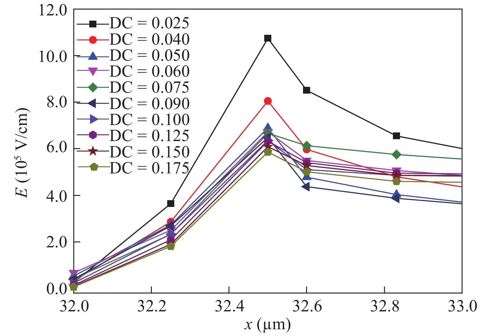
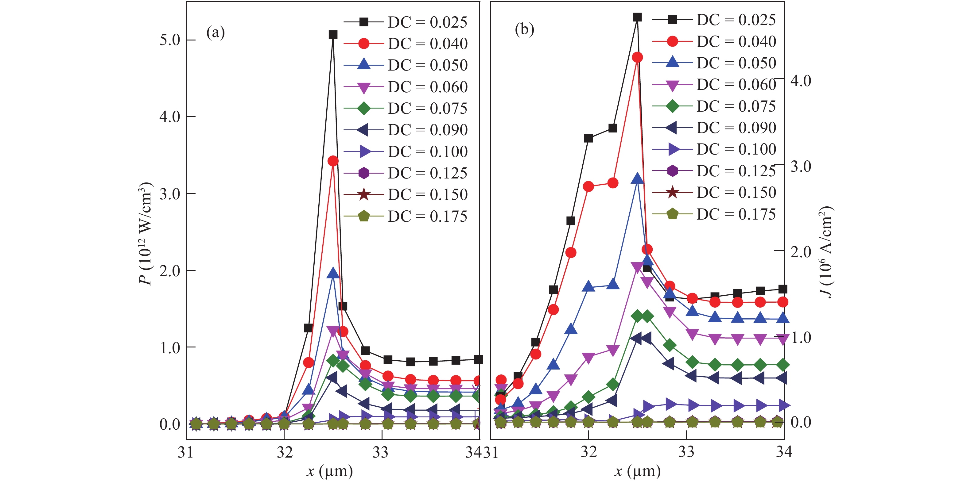
Abstract: Theoretical research on the heat accumulation effect of a Darlington transistor induced by high power microwave is conducted, and temperature variation as functions of pulse repetitive frequency (PRF) and duty cycle (DC) are studied. According to the distribution of the electronic field and the current density in the Darlington transistor, the research of the damage mechanism is carried out. The results show that for repetitive pulses with the same pulse widths and different PRFs, the value of temperature variation increases with PRF increases, and the peak temperature has almost no change when PRF is lower than 200 kHz; while for the repetitive pulses with the same PRF and different pulse widths, the larger the pulse width is, the greater temperature variation varies. The response of the peak temperature caused by a single pulse demonstrates that there is no temperature variation when the rising time is much shorter than the falling time. In addition, the relationship between the temperature variation and the time during the rising edge time as well as that between the temperature variation and the time during the falling edge time are obtained utilizing the curve fitting method. Finally, for a certain average power, with DC increases the value of temperature variation decreases.

Key words: Darlington transistorhigh power microwavepulse repetitive frequencyduty cycle

As integrated circuits and semiconductor devices become smaller, the electronic equipment and components are susceptible to microwave pulses. A variety of microwave pulses can cause the failure and even destruction of electronic equipment and components[19]. A lot of work has been done in the fields of electronic system damage and device damage, some of which focus on the effects of pulse parameters on device damage. Different measurements are proposed to study the effect of ultra wide bandwidth (UWB) and radar pulses on the receiver of a digital wireless communication system[10]. The findings show that Bluetooth communication has the ability to transmit data up to the PRF of 2 kHz, while WLAN communication is able to transmit data up to the PRF of 3.5 kHz , and a high PRF and pulse lengths can make both communication links damaged. In Ref. [11], Daniel et al. provide an overview of the susceptibility of many various electronic devices, the findings demonstrate that many types of electronic equipment, including logic devices, microprocessor boards, PC networks, and microprocessor boards, are caused by electromagnetic pulse (EMP), high power microwave (HPM) pulses, and UWB. The analysis presents that a lower field strength can only damage electronic components such as transistors or diodes on the chip, while a higher amplitude is needed to destroy the band wire, multiple component, and chip wire. The Swedish Defence Authorities have searched for the effects of high power microwave radiation on the electronic systems including military equipment and civil equipment[12]. The results manifest that the distance for the damage of HPM can reach approximately one kilometer. In addition, the pulse width and the PRF are crucial for some types of disturbance, and the first pulse of a pulse train usually leads to the permanent damage. In Ref. [13], Ma et al. injected pulsed microwaves with different PRF and duty cycles (DCs) into the output of a bipolar transistor; the results indicate that the pulses with lower PRF cannot lead to any thermal stacking within the device, and increasing the PRF can cause more accumulating temperature, in addition, they found that with rising DC the accumulating temperature falls.

Researchers pay more attention to the damage of an electronic system level caused by HPM and EMP, while fewer researchers have analysed theoretically the device damage level caused by HPM and EMP. The Darlington transistor has significant applications in power amplifier circuits, power circuits, switching circuits, drive small type relay circuits, drive LED intelligence display screen circuits, etc. Although new structures and new materials are brought up to improve the working efficiency of the Darlington transistor, less study has been carried out on the damage of the Darlington transistor induced by HPM and EMP. In this paper, a two-dimensional electron-thermal model of the silicon PNP type Darlington transistor is established using the device simulator Sentaurus-TCAD. The output-input characteristic curves are obtained firstly, then the damage effect and mechanism caused by repetitive pulse is discussed. Finally, the relationship between the heat accumulation effect caused by HPM and pulsed parameters such as PRF and DC are studied.

The equivalent circuit of the PNP type Darlington transistor is presented in Fig. 1, E, B, and C represent the emitter, base, and collector of the device, respectively. T1 and T2 represent two PNP transistors of the same power, specially, T1 is called the first stage transistor, while T2 is defined as the second stage transistor. Fig. 2 shows the structure of the device in this paper. Since these two PNP transistors are the same, hence we just list the parameters of the T1 transistor. The horizontal width of the emitter and the base of the T1 transistor are 8 and 20 μm, respectively. P1+ is the emitter region of the T1 transistor where the doping method is Gauss doping with doped impurity of the Boron element and a surface concentration of 1 × 1020 cm−3, N1 is the base region of the T1 transistor where the doping mode is uniform doping with doped impurity of the Phosphorus element and the doping concentration of 1 × 1017 cm−3. The emitter junction and the base junction of the T1 transistor are 0.4 and 0.8 μm. It is noted that the collector of the Darlington transistor is shared by the T1 and T2 transistors. P-epi is the 2-μm-thick p-type epitaxial layer with doped impurity of the Phosphorus element and the doping concentration of 5 × 1015 cm−3. P+-sub represent the 12-μm-thick collector substrate of p-type silicon with doped impurity of the Phosphorus element and the doping concentration of 5 × 1019 cm−3. The thermal electrode is specified at the bottom of the device (along line y = 14 μm), in which the lattice temperature is assumed to be a constant of 300 K. In addition, the sidewall boundaries (along lines x = 0 and x = 40.5 μm) and the upper surface are thermally insulated from the environment.

Figure  1.  Circuit schematic of PNP type Darlington transistor.
Figure  2.  Two dimensional sectional view of structure of PNP type Darlington transistor.

In this paper, the device simulator is used to calculate the electronic behavior of the Darlington transistor by iteratively solving the Poisson equation, the current-continuity equations[14]. High current and high voltage generated by the injected signals would produce a huge Joule heat during the injection of the repetitive pulse, which leads to a significant temperature variation within the Darlington transistor. Considering the influence of the internal self-heating effect on the device, the heat of the equation should be calculated:

cTtkT=[(PnT+ϕn)Jn+(PpT+ϕp)Jp](EC+32kBT)Jn(EV32kBT)Jp+qR(ECEV+3kBT), (1)

in which c is the lattice heat capacity, k is the thermal conductivity, Jn and Jp are the electron and hole current density, respectively. EC and EV are the conduction and valence band energy, respectively, kB denotes the Boltzmann constant and R is the recombination rate. In addition, the thermodynamic model is adopted assuming that the charge carriers are in thermal equilibrium with the lattice. SRH recombination, Auger recombination, and the Avalanche breakdown model are taken into account in generation and recombination of the charge carrier.

In this paper, the square pulse modulated sinusoidal signals with the carrier frequency of 1 GHz are used[15], and the device is considered to have failed when the peak temperature of the device reaches the melting point of silicon (1688 K).

The simulation circuit is shown in Fig. 3, where the Darlington transistor is in the active mode of operation. The input-output characteristic curve of the device is obtained and plotted in Fig. 4, therefore, the quiescent DC operation point is set to VCEQ = −6.5 V, ICQ = −0.3 mA, VBEQ = −1.4 V, IBQ = −0.4 μA, and the values of VCC, Rb, and Rc are set to −9.0 V, 19.0 MΩ, and 8.3 kΩ, respectively according to the equations below:

Figure  4.  (Color online) The input–output characteristic curve of Darlington transistor.
Rb=VccVBEQIBQ, (2)
Rc=VccVCEQICQ. (3)

To investigate the heat accumulation effect of the Darlington transistor caused by repetitive pulse, the square wave pulse modulated sinusoidal signals with a PRF of 10 MHz and a pulse width of 60 ns are injected into the output of the device. The frequency and the amplitude of the carrier are 1 GHz and 15 V, respectively. Fig. 5 depicts the relationship between peak temperature and simulation time within the first five cycles. As we can see from the figure the peak temperature increases within the square pulse and decreases in the pulse intervals. The peak temperature variation presents a tendency of increase–decrease, on the whole, the peak temperature rises versus the simulation time until the Darlington transistor is destroyed.

Figure  5.  (Color online) The peak temperature within the device and the injected signal as a function of simulation time.

In this section, the repetitive pulse signals with a pulse width of 60 ns and different PRF from 50 kHz to 10 MHz are injected into the device. Fig. 6 shows the variation of peak temperature, ΔT, with time when PRFs are 0.1, 1, 5, and 10 MHz, respectively. ΔT is defined as the difference between the value of peak temperature at the end of the fifth period and the ambient temperature. It can be seen from Fig. 6 that with decreasing the PRF the value of ΔT is decreasing too. The value of ΔT is 81.0 K when PRF is 10 MHz, while the value of ΔT drops to 10.0 K when the PRF decreases to 1 MHz. Note that the value of ΔT is only 4.3 K at the end of every pulse when the PRF is 100 kHz, demonstrating that heat accumulation hardly exists within the Darlington transistor, that is to say, this kind of repetitive pulse cannot destroy the Darlington transistor established in this paper.

Figure  6.  (Color online) The relationship between peak temperature and time with different PRF which are (a) 10 MHz, (b) 5 MHz, (c) 1 MHz, and (d) 100 kHz, respectively.

Repetitive pulse signals (pulse widths are 20, 40, 60, and 80 ns, respectively) with PRF varying from 50 kHz to 10 MHz are injected into the output of the device, and Fig. 7 presents the simulation results.

Figure  7.  (Color online) Curves of temperature increment versus PRF for pulse widths of 20, 40, 60, and 80 ns, respectively.

As shown in Fig. 7, for the repetitive pulse with the same pulse width, the relationship between ΔT and PRF can be divided into three parts. In the first part, the value of ΔT is a constant of 4.3 K when PRF is less than 200 kHz, which means that there has been no heat accumulation within the device in this case. In the second stage, it can be seen clearly that ΔT presents a linear relationship dependence on the PRF which varies from 200 kHz to 4 MHz. For the last part, it shows a quasi-linear relationship between ΔT and PRF when the PRF is larger than 4 MHz but smaller than 10 MHz. For instance, the piecewise function for the interference signal with a pulse width of 60 ns can be obtained:

ΔT={4.3,0<f<200kHz,1.1×105f0.3,200kHzf<4MHz,6.4×106f+18.1,4MHzf<10MHz, (4)

of which the correlation coefficients (R2) of the second equation and the third equation are 0.999 and 0.993 respectively, which shows high degrees of fitting. Besides, we can form a conclusion from the figure that for the pulse with the same PRF, the wider the pulse width is, the larger the value of ΔT is.

To study the effects of the single pulse interference signal on the device damage, Fig. 8 shows the response of peak temperature versus time when single pulses with pulse widths of 20, 40, 60, and 80 ns, respectively are injected.

Figure  8.  (Color online) The response of peak temperature of the Darlington transistor versus time for single pulses with different pulse widths.

As we can see from Fig. 8, the duration of temperature rising is much less than that of temperature decreasing, and the peak temperature would drop to 304.3 K in approximately 4.0 μs after removing the single pulse signals, which means that there has been no heat accumulation within the Darlington transistor if the PRF is smaller than 250 kHz; this conclusion is consistent with the above analysis. For the sake of a better understanding of the relationship between the peak temperature and the time, we obtain the corresponding relations of the four rising edges:

{T20ns=296.5+89.0×{(1exp[t/(3.0×108)]}T40ns=296.1+76.4×{(1exp[t/(2.4×108)]}T60ns=297.2+81.2×{(1exp[t/(2.8×108)]}T80ns=298.4+85.0×{(1exp[t/(3.2×108)]}, (5)

where R2 are 0.982, 0.993, 0.995, and 0.996, respectively, presenting good degrees of fitting. For the different falling edges, the curves with four various pulse widths are also fitted and expressed as:

{T20ns=304.3+39.4×exp[t/(8.0×108)]T40ns=304.3+67.7×exp[t/(1.3×107)]T60ns=304.3+91.2×exp[t/(1.5×107)]T80ns=304.3+111.7×exp[t/(1.8×107)], (6)

of which R2 are 0.993, 0.995, 0.996, and 0.997, respectively, showing good degrees of fitting. It can be found that both rising edges and falling edges obey abnormal exponential progression. For curves of falling edge, the equations all comply with the rules:

T=A+B(T)×exp(t/τth), (7)

where A is a constant of 304.3 K, and B(T) is a constant connected with the temperature of the device. For the constant of τth, it is a function of temperature[16], the initial temperatures of the falling edge are different for different pulse widths, hence the values of τth are different for different pulse widths, too. According to this equation, we can predict the temperature variation within the Darlington transistor under the injections of single pulses with different pulse widths.

The influence of duty cycle on the peak temperature variation is studied because DC is a significant parameter of a repetitive pulse. The schematic diagram of the simulation circuit is shown in Fig. 3. The interference signals with an average power of 1.2 × 10³ W and a PRF of 5 MHz are injected into the Darlington transistor from the output, and the DC of the repetitive pulse varies from 0.025 to 0.175. Fig. 9 depicts the relationship between ΔT and DC, as we can see from this figure that the value of ΔT significantly falls as DC rises. The value of ΔT is 149.0 K when DC is 0.025, while it drops to 3.2 K when DC is 0.175. In addition, we can clearly see that there is little temperature accumulation (approximately 3.0 K) when DC is lower than 0.15.

Figure  9.  Temperature variation as a function of duty cycle for a certain average power.
Figure  3.  Schematic diagram of the simulation circuit.

Temperature elevation occurs in the positive half-period of the sinusoidal signal and the damage location is in the cylindrical region of the base-emitter junction of the T2 transistor. The variations of electric field (E) as a function of the x axis (along the line y = 0.3 μm), with the repetitive pulse with different duty cycles injected at the moment of 4.75 ns, is shown in Fig. 10. With increasing duty cycle, the value of E at the position of x = 32.5 μm (damage position) is decreasing. The value of E (1.1 × 10⁶ V/cm) with DC = 0.025 is approximately two times larger than that of E (5.1 × 10⁵ V/cm) with DC = 0.175. The mean power is proportional to DC and the square of the voltage:

PDCU20. (8)

Because the average power is a definite value, the larger the DC is, the smaller the U0 is. As we know, the value of E is proportional to U0, in other words, the value of E which is at the position of x = 32.5 μm decreases with the decreases of the U0. Through the above analysis in theory, we can make a conclusion that the larger the DC is, the smaller the value of E at the damage position is, which is consistent with the simulation results presented in Fig. 10 at the moment of 4.75 ns for different duty cycles (along the line y = 0.3 μm).

Figure  10.  (color online) Electronic field across damage position at the moment of 4.75 ns for different duty cycles (along the line y = 0.3 μm).

Fig. 11(a) shows the current density (J) across the damage location (along the line y = 0.3 μm) at 4.75 ns. From Fig. 11(a), it can be seen that with decreasing duty cycle the value of J, which is at the damage position, increases. We know that the value of U0 increases as DC decreases, and a higher voltage causes a larger current density at the position of x = 32.5 μm. In addition, the figure shows that the values of the current density at the damage position are almost equal to zero when DC is larger than 0.125, the reason is that a voltage less than a certain value cannot produce a high current for the Darlington transistor in this paper.

Figure  11.  (color online) (a) Instantaneous power density and (b) current density across damage position at the moment of 4.75 ns for different duty cycles (along the line y = 0.3 μm).

The instantaneous power density (P) across the damage location (along the line y = 0.3 μm) at 4.75 ns is presented in Fig. 11(b). P is defined as the product of the electric field E and the current density J. As Fig. 11(b) shows, firstly, the value of P decreases at the damage position of x = 32.5 μm with the rise of DC. P is approximately 5.1 × 10¹² W/cm3 when DC is 0.025, however, when DC increases to 0.125, P is only about 5.8 × 10⁸ W/cm3. Secondly, the value of P is so small at the damage position that it can be negligible when DC is larger than 0.125. Therefore, this conclusion can account for the phenomenon that temperature variation ΔT in the damage position is small when the Darlington transistor is injected into a repetitive pulse with a DC of higher than 0.125.

In this paper, we established a two-dimensional electron-thermal model of the silicon PNP type Darlington transistor utilizing the device simulator. Firstly, the damage effect of the device which is induced by the repetitive pulse signals with different PRFs and duty cycles is investigated. The results demonstrate that the temperature variation has a periodic rule of decrease-increase. For the repetitive pulse with the same pulse width, with PRF increases the value of temperature variation increases; while for the repetitive pulse with the same PRF, the larger the value of pulse width is, the higher the value of temperature variation is. Secondly, the damage laws of the device caused by a single pulse with pulse width from 20 to 80 ns are obtained, which shows that there is little temperature accumulation within the device when PRF is lower than approximately 200 kHz , in other words, the Darlington transistor will not be destroyed by the interference signals if the device is not destroyed in the first pulse of a pulse train in this case. Finally, the effect of DC on temperature variation is studied. The result presents that temperature variation decreases with the DC rises. The reason for this result is that the values of electronic field E and the current J density at the damage position fall as the DC rises, which leads to the value of power density P decreasing with the DC increasing. The conclusions obtained from this paper can predict the damage effect of the Darlington transistor caused by some specific pulse interference signals.


[1]
Krzikalla R, Luiken J, Ter Haneborg L, et al. Systematic description of the protection capability of protection elements. IEEE International Symposium on Electromag Compat, 2007, 179: 1
[2]
Bayram Y, Chang P C, Volakis J L, et al. High power EMI on digital circuits within automotive structures. IEEE Int Symp Electromagn Compat, 2006, 2: 507
[3]
Hwang S M, Hong J I, Huh C S. Characterization of susceptibility of integrated circuits with induction caused by high power microwaves. Prog Electromagn Res, 2008, 81: 61 doi: 10.2528/PIER07121704
[4]
Mansson D, Thottappillil R, Nilsson T, et al. Susceptibility of civilian GPS receivers to electromagnetic radiation. IEEE Trans Electromagn Compat, 2008, 50(2): 434 doi: 10.1109/TEMC.2008.921015
[5]
Sabath F, Backstrom M, Nordstrom B, et al. Overview of four European high-power microwave narrow-band test facilities. IEEE Trans Electromagn Compat, 2004, 46(3): 329 doi: 10.1109/TEMC.2004.831822
[6]
Fan J P, Zhang L, Jia X Z. HPM damage mechanism on bipolar transistors. High Power Laser Part. Beams, 2010, 22: 1319 doi: 10.3788/HPLPB
[7]
Radasky W A, Baum C E, Wik M W. Introduction to the special issue on high-power electromagnetics (HPEM) and intentional electromagnetics interference (IEMI). IEEE Trans Electromagn Compat, 2004, 46(3): 314 doi: 10.1109/TEMC.2004.831899
[8]
Ma Z Y, Chai C C, Ren X R, et al. Effects of microwave pulse-damage on a bipolar transistor. Chin Phys B, 2012, 21: 058502 doi: 10.1088/1674-1056/21/5/058502
[9]
Ma Z Y, Chai C C, Ren X R, et al. Microwave damage susceptibility trend of a bipolar transistor as a function of frequency. Chin Phys B, 2012, 21: 098502 doi: 10.1088/1674-1056/21/9/098502
[10]
Klunder C, Haneborg J L. Effects of high-power and transient disturbances on wireless communication systems operating inside the 2.4 GHz ISM band. IEEE Int Symp Electromagn Compat Fort Lauderdale, FL, USA, 2010, 359
[11]
Nitsch D, Camp M, Sabath F, et al. Susceptibility of some electronic equipment to HPEM threats. IEEE Trans Electromagn Compat, 2004, 46(3): 380 doi: 10.1109/TEMC.2004.831842
[12]
BackStrom M G, Lovstrand K G. Susceptibility of electronic system by high power microwave: summary of test experience. IEEE Trans Electromagn Compat, 2004, 46(3): 396 doi: 10.1109/TEMC.2004.831814
[13]
Ma Z Y, Chai C C, Ren X R, et al. The pulsed microwave damage trend of a bipolar transistor as a function of pulse parameters. Chin Phys B, 2013, 22: 028502 doi: 10.1088/1674-1056/22/2/028502
[14]
Integrated Systems Engineering Corp. ISE-TCAD Dessis Simulation Users Manual, Zurich, Switzerland, 2004, 142
[15]
Radasky W A. Protection of commercial installations from the high-frequency electromagnetic threats of HEPM and IEMI using IEC standards. Asia-Pacific Symposium on Electromagnetic Compatibility, Beijing, China, 2010: 758
[16]
Anghel C, Gillon R, Ionescu A M. Self-heating characterization and extraction method for thermal resistance and capacitance. IEEE Electron Device Lett, 2004, 25(3): 141 doi: 10.1109/LED.2003.821669
Fig. 1.  Circuit schematic of PNP type Darlington transistor.

Fig. 2.  Two dimensional sectional view of structure of PNP type Darlington transistor.

Fig. 4.  (Color online) The input–output characteristic curve of Darlington transistor.

Fig. 5.  (Color online) The peak temperature within the device and the injected signal as a function of simulation time.

Fig. 6.  (Color online) The relationship between peak temperature and time with different PRF which are (a) 10 MHz, (b) 5 MHz, (c) 1 MHz, and (d) 100 kHz, respectively.

Fig. 7.  (Color online) Curves of temperature increment versus PRF for pulse widths of 20, 40, 60, and 80 ns, respectively.

Fig. 8.  (Color online) The response of peak temperature of the Darlington transistor versus time for single pulses with different pulse widths.

Fig. 9.  Temperature variation as a function of duty cycle for a certain average power.

Fig. 3.  Schematic diagram of the simulation circuit.

Fig. 10.  (color online) Electronic field across damage position at the moment of 4.75 ns for different duty cycles (along the line y = 0.3 μm).

Fig. 11.  (color online) (a) Instantaneous power density and (b) current density across damage position at the moment of 4.75 ns for different duty cycles (along the line y = 0.3 μm).

[1]
Krzikalla R, Luiken J, Ter Haneborg L, et al. Systematic description of the protection capability of protection elements. IEEE International Symposium on Electromag Compat, 2007, 179: 1
[2]
Bayram Y, Chang P C, Volakis J L, et al. High power EMI on digital circuits within automotive structures. IEEE Int Symp Electromagn Compat, 2006, 2: 507
[3]
Hwang S M, Hong J I, Huh C S. Characterization of susceptibility of integrated circuits with induction caused by high power microwaves. Prog Electromagn Res, 2008, 81: 61 doi: 10.2528/PIER07121704
[4]
Mansson D, Thottappillil R, Nilsson T, et al. Susceptibility of civilian GPS receivers to electromagnetic radiation. IEEE Trans Electromagn Compat, 2008, 50(2): 434 doi: 10.1109/TEMC.2008.921015
[5]
Sabath F, Backstrom M, Nordstrom B, et al. Overview of four European high-power microwave narrow-band test facilities. IEEE Trans Electromagn Compat, 2004, 46(3): 329 doi: 10.1109/TEMC.2004.831822
[6]
Fan J P, Zhang L, Jia X Z. HPM damage mechanism on bipolar transistors. High Power Laser Part. Beams, 2010, 22: 1319 doi: 10.3788/HPLPB
[7]
Radasky W A, Baum C E, Wik M W. Introduction to the special issue on high-power electromagnetics (HPEM) and intentional electromagnetics interference (IEMI). IEEE Trans Electromagn Compat, 2004, 46(3): 314 doi: 10.1109/TEMC.2004.831899
[8]
Ma Z Y, Chai C C, Ren X R, et al. Effects of microwave pulse-damage on a bipolar transistor. Chin Phys B, 2012, 21: 058502 doi: 10.1088/1674-1056/21/5/058502
[9]
Ma Z Y, Chai C C, Ren X R, et al. Microwave damage susceptibility trend of a bipolar transistor as a function of frequency. Chin Phys B, 2012, 21: 098502 doi: 10.1088/1674-1056/21/9/098502
[10]
Klunder C, Haneborg J L. Effects of high-power and transient disturbances on wireless communication systems operating inside the 2.4 GHz ISM band. IEEE Int Symp Electromagn Compat Fort Lauderdale, FL, USA, 2010, 359
[11]
Nitsch D, Camp M, Sabath F, et al. Susceptibility of some electronic equipment to HPEM threats. IEEE Trans Electromagn Compat, 2004, 46(3): 380 doi: 10.1109/TEMC.2004.831842
[12]
BackStrom M G, Lovstrand K G. Susceptibility of electronic system by high power microwave: summary of test experience. IEEE Trans Electromagn Compat, 2004, 46(3): 396 doi: 10.1109/TEMC.2004.831814
[13]
Ma Z Y, Chai C C, Ren X R, et al. The pulsed microwave damage trend of a bipolar transistor as a function of pulse parameters. Chin Phys B, 2013, 22: 028502 doi: 10.1088/1674-1056/22/2/028502
[14]
Integrated Systems Engineering Corp. ISE-TCAD Dessis Simulation Users Manual, Zurich, Switzerland, 2004, 142
[15]
Radasky W A. Protection of commercial installations from the high-frequency electromagnetic threats of HEPM and IEMI using IEC standards. Asia-Pacific Symposium on Electromagnetic Compatibility, Beijing, China, 2010: 758
[16]
Anghel C, Gillon R, Ionescu A M. Self-heating characterization and extraction method for thermal resistance and capacitance. IEEE Electron Device Lett, 2004, 25(3): 141 doi: 10.1109/LED.2003.821669
1

Layer-number dependent high-frequency vibration modes in few-layer transition metal dichalcogenides induced by interlayer couplings

Qing-Hai Tan, Xin Zhang, Xiang-Dong Luo, Jun Zhang, Ping-Heng Tan, et al.

Journal of Semiconductors, 2017, 38(3): 031006. doi: 10.1088/1674-4926/38/3/031006

2

Zinc-doped CdS nanoparticles synthesized by microwave-assisted deposition

Abideen A. Ibiyemi, Ayodeji O Awodugba, Olusola Akinrinola, Abass A Faremi

Journal of Semiconductors, 2017, 38(9): 093002. doi: 10.1088/1674-4926/38/9/093002

3

A prediction technique for single-event effects on complex integrated circuits

Yuanfu Zhao, Chunqing Yu, Long Fan, Suge Yue, Maoxin Chen, et al.

Journal of Semiconductors, 2015, 36(11): 115003. doi: 10.1088/1674-4926/36/11/115003

4

Modeling and analysis of the HPM pulse-width upset effect on CMOS inverter

Xinhai Yu, Changchun Chai, Liping Qiao, Yintang Yang, Yang Liu, et al.

Journal of Semiconductors, 2015, 36(5): 054011. doi: 10.1088/1674-4926/36/5/054011

5

Hysteresis analysis of graphene transistor under repeated test and gate voltage stress

Jie Yang, Kunpeng Jia, Yajuan Su, Yang Chen, Chao Zhao, et al.

Journal of Semiconductors, 2014, 35(9): 094003. doi: 10.1088/1674-4926/35/9/094003

6

Performance analysis of silicon nanowire transistors considering effective oxide thickness of high-k gate dielectric

S. Theodore Chandra, N. B. Balamurugan

Journal of Semiconductors, 2014, 35(4): 044001. doi: 10.1088/1674-4926/35/4/044001

7

A high power active circulator using GaN MMIC power amplifiers

Liming Gu, Wenquan Che, Fan-Hsiu Huang, Hsien-Chin Chiu

Journal of Semiconductors, 2014, 35(11): 115003. doi: 10.1088/1674-4926/35/11/115003

8

Dynamic threshold voltage operation in Si and SiGe source junctionless tunnel field effect transistor

Shibir Basak, Pranav Kumar Asthana, Yogesh Goswami, Bahniman Ghosh

Journal of Semiconductors, 2014, 35(11): 114001. doi: 10.1088/1674-4926/35/11/114001

9

Temperature dependence of latch-up effects in CMOS inverter induced by high power microwave

Xinhai Yu, Changchun Chai, Xingrong Ren, Yintang Yang, Xiaowen Xi, et al.

Journal of Semiconductors, 2014, 35(8): 084011. doi: 10.1088/1674-4926/35/8/084011

10

Chaotic dynamics dependence on doping density in weakly coupled GaAs/AlAs superlattices

Yang Gui, Li Yuanhong, Zhang Fengying, Li Yuqi

Journal of Semiconductors, 2012, 33(9): 092002. doi: 10.1088/1674-4926/33/9/092002

11

A low power cyclic ADC design for a wireless monitoring system for orthopedic implants

Chen Yi, Li Fule, Chen Hong, Zhang Chun, Wang Zhihua, et al.

Journal of Semiconductors, 2009, 30(8): 085009. doi: 10.1088/1674-4926/30/8/085009

12

High-performance micromachined gyroscope with a slanted suspension cantilever

Xiao Dingbang, Wu Xuezhong, Hou Zhanqiang, Chen Zhihua, Dong Peitao, et al.

Journal of Semiconductors, 2009, 30(4): 044012. doi: 10.1088/1674-4926/30/4/044012

13

A Piecewise Linear Slope Compensation Circuit for DC-DC Converters

Ye Qiang, Lai Xinquan, Li Yanming, Yuan Bing, Chen Fuji, et al.

Journal of Semiconductors, 2008, 29(2): 281-287.

14

Low-Microwave Loss Coplanar Waveguides Fabricated on High-Resistivity Silicon Substrate

Yang Hua, Zhu Hongliang, Xie Hongyun, Zhao Lingjuan, Zhou Fan, et al.

Chinese Journal of Semiconductors , 2006, 27(1): 1-4.

15

Design and Fabrication of Power Si1-xGex/Si Heterojunction Bipolar Transistor for Wireless Power Amplifier Applications

Xue Chunlai, Cheng Buwen, Yao Fei, Wang Qiming

Chinese Journal of Semiconductors , 2006, 27(1): 9-13.

16

An Optoelectronic Pulse Frequency Modulation Circuitfor Retinal Prosthesis

Liu Jinbin, Chen Hongda, Gao Peng, Pei Weihua, Sui Xiaohong, et al.

Chinese Journal of Semiconductors , 2006, 27(4): 700-704.

17

Temperature Dependence of Vacuum Rabi Splitting in a Single Quantum Dot-Semiconductor Microcavity

Zhu Kadi, Li Waisang

Chinese Journal of Semiconductors , 2006, 27(3): 489-493.

18

Design and Simulation of a Light-Activated Darlington Transistor Based on a SiCGe/3C-SiC Hetero-Structure

Chen Zhiming, Ren Ping, Pu Hongbin

Chinese Journal of Semiconductors , 2006, 27(2): 254-257.

19

Passively Mode Locked Diode-End-Pumped Yb∶YAB Laser with High Reflectivity Type Semiconductor Saturable Absorption Mirror

Wang Yonggang, Ma Xiaoyu, Xue Yinghong, Sun Hong,Zhang Zhigang,and Wang Qingyue

Chinese Journal of Semiconductors , 2005, 26(2): 250-253.

20

AIN Monolithic Microchannel Cooled Heatsink for High Power Laser Diode Array

Ma Jiehui, Fang Gaozhan, Lan Yongsheng and, Ma Xiaoyu

Chinese Journal of Semiconductors , 2005, 26(3): 476-479.

1. Jin, W., Chai, C., Liu, Y. et al. Microwave damage susceptibility trend of the silicon npn monolithic composite transistor as a function of structure parameters | [硅基单片式复合晶体管的结构参数对高功率微波损伤效应的影响(英)]. Qiangjiguang Yu Lizishu/High Power Laser and Particle Beams, 2019, 31(10): 103220. doi:10.11884/HPLPB201931.190218
  • Search

    Advanced Search >>

    GET CITATION

    Qiankun Wang, Changchun Chai, Yuqian Liu, Yintang Yang. The influence of pulsed parameters on the damage of a Darlington transistor[J]. Journal of Semiconductors, 2018, 39(9): 094005. doi: 10.1088/1674-4926/39/9/094005
    Q K Wang, C C Chai, Y Q Liu, Y T Yang, The influence of pulsed parameters on the damage of a Darlington transistor[J]. J. Semicond., 2018, 39(9): 094005. doi: 10.1088/1674-4926/39/9/094005.
    shu

    Export: BibTex EndNote

    Article Metrics

    Article views: 3931 Times PDF downloads: 36 Times Cited by: 1 Times

    History

    Received: 27 November 2017 Revised: 24 April 2018 Online: Uncorrected proof: 16 May 2018Accepted Manuscript: 05 July 2018Published: 01 September 2018

    Catalog

      Email This Article

      User name:
      Email:*请输入正确邮箱
      Code:*验证码错误
      Qiankun Wang, Changchun Chai, Yuqian Liu, Yintang Yang. The influence of pulsed parameters on the damage of a Darlington transistor[J]. Journal of Semiconductors, 2018, 39(9): 094005. doi: 10.1088/1674-4926/39/9/094005 ****Q K Wang, C C Chai, Y Q Liu, Y T Yang, The influence of pulsed parameters on the damage of a Darlington transistor[J]. J. Semicond., 2018, 39(9): 094005. doi: 10.1088/1674-4926/39/9/094005.
      Citation:
      Qiankun Wang, Changchun Chai, Yuqian Liu, Yintang Yang. The influence of pulsed parameters on the damage of a Darlington transistor[J]. Journal of Semiconductors, 2018, 39(9): 094005. doi: 10.1088/1674-4926/39/9/094005 ****
      Q K Wang, C C Chai, Y Q Liu, Y T Yang, The influence of pulsed parameters on the damage of a Darlington transistor[J]. J. Semicond., 2018, 39(9): 094005. doi: 10.1088/1674-4926/39/9/094005.

      The influence of pulsed parameters on the damage of a Darlington transistor

      DOI: 10.1088/1674-4926/39/9/094005
      Funds:

      Project supported by the Open Fund of Key Laboratory of Complex Electromagnetic Environment Science and Technology, China Academy of Engineering Physics (No. 2015-0214.XY.K).

      More Information
      • Corresponding author: Email: wang__qk@163.com
      • Received Date: 2017-11-27
      • Revised Date: 2018-04-24
      • Published Date: 2018-09-01

      Catalog

        /

        DownLoad:  Full-Size Img  PowerPoint
        Return
        Return