Fig. 1.
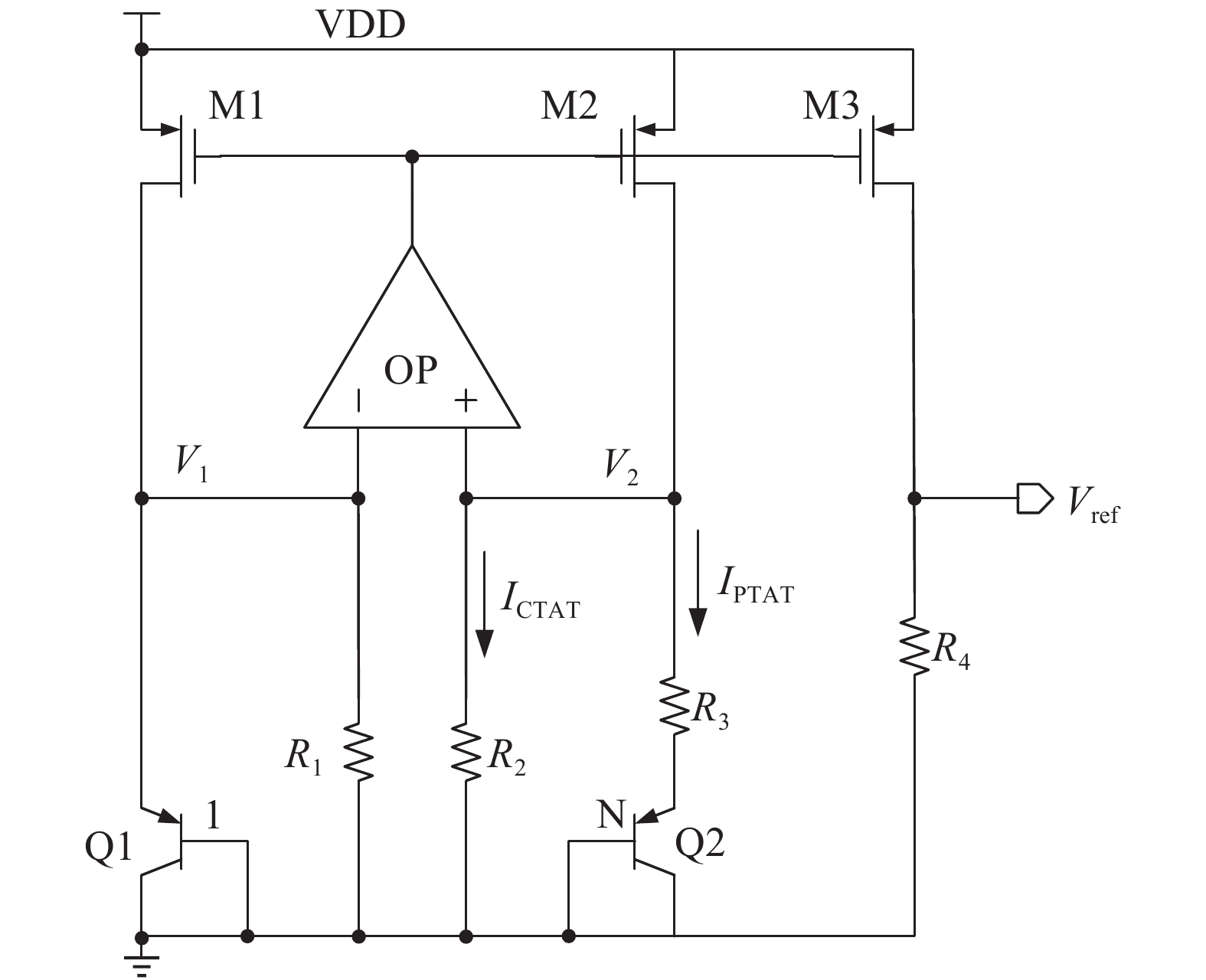
Conventional bandgap reference circuit.
SEMICONDUCTOR INTEGRATED CIRCUITS
Jing Leng1, Yangyang Lu1, Yunwu Zhang1, 2, Huan Xu1, Kongsheng Hu1, Zhicheng Yu1, Weifeng Sun1, and Jing Zhu1
Corresponding author: Weifeng Sun, Email: swffrog@seu.edu.cn
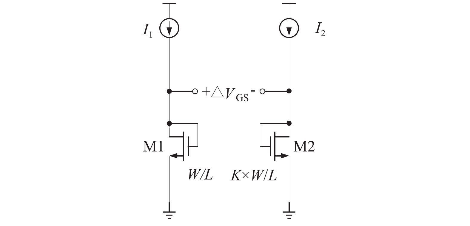
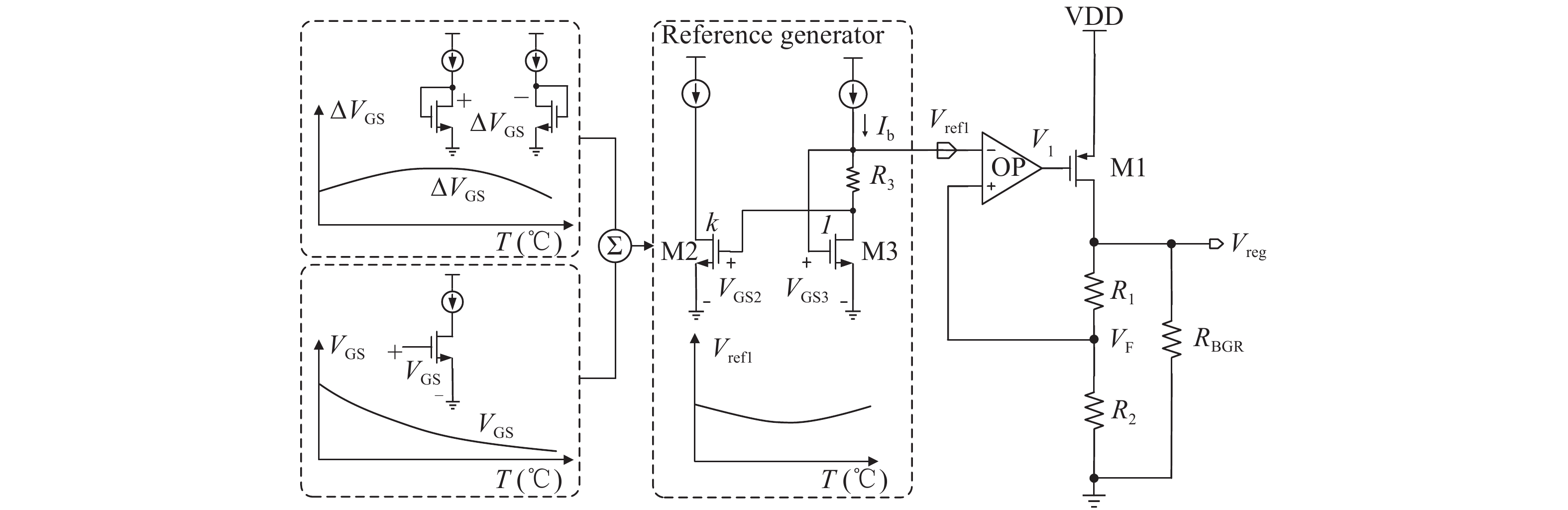
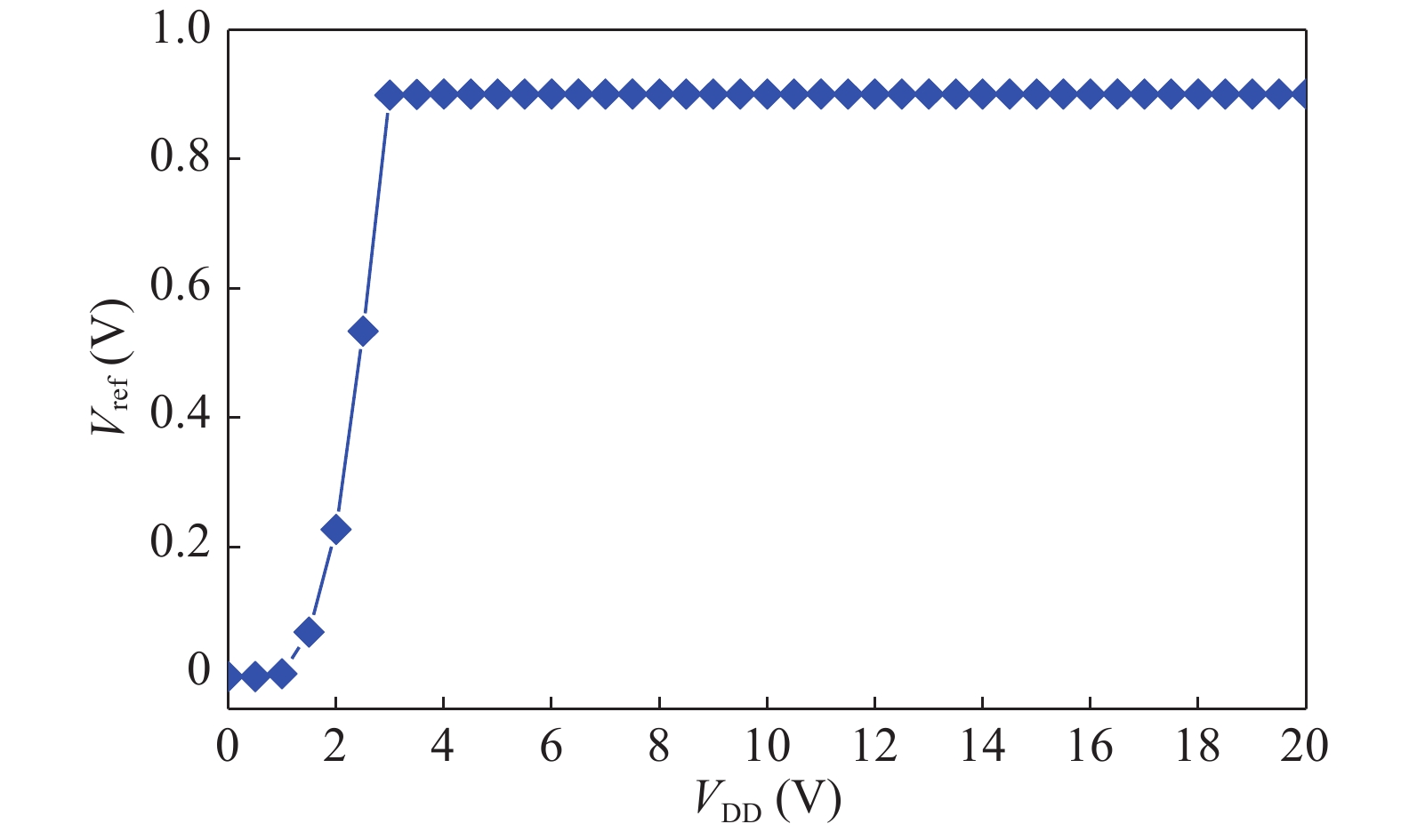
Abstract: A high-order curvature-compensated CMOS bandgap reference (BGR) topology with a low temperature coefficient (TC) over a wide temperature range and a high power supply reject ratio (PSRR) is presented. High-order correction is realized by incorporating a nonlinear current INL, which is generated by ∆VGS across resistor into current generated by a conventional first-order current-mode BGR circuit. In order to achieve a high PSRR over a broad frequency range, a voltage pre-regulating technique is applied. The circuit was implemented in CSMC 0.5 μm 600 V BCD process. The experimental results indicate that the proposed topology achieves TC of 0.19 ppm/°C over the temperature range of 165 °C (−40 to 125 °C), PSRR of −123 dB @ DC and −56 dB @ 100 kHz. In addition, it achieves a line regulation performance of 0.017%/V in the supply range of 2.8–20 V.
Keywords: bandgap reference (BGR), temperature coefficient (TC), power supply rejection ratio (PSRR)
| [1] |
Song B S, Gray P R. A precision curvature-compensated CMOS bandgap reference. IEEE J Solid-State Circuits, 1983, 18(6): 634 doi: 10.1109/JSSC.1983.1052013
|
| [2] |
Vogler B, Rosberg M, Herzer R. A fully integrated 600 V SOI half bridge IGBT gate driver IC. 51th IWK, Internationales Wissenschaftliches Kolloquium, 2006
|
| [3] |
Rincon-Mora G, Allen P E. A 1.1-V current-mode and piecewise-linear curvature-corrected bandgap reference. IEEE J Solid-State Circuits, 1998, 33(10): 1551 doi: 10.1109/4.720402
|
| [4] |
Huang Y, Cheung C, Najafizadeh L. A multi-piecewise curvature-corrected technique for bandgap reference circuits. 2013 IEEE 56th International Midwest Symposium on Circuits and Systems (MWSCAS), 2013: 305
|
| [5] |
Wang R, Lu W, Zhao M, et al. A 2.1-ppm/°C current-mode CMOS bandgap reference with piecewise curvature compensation. 2017 IEEE International Symposium on Circuits and Systems (ISCAS), 2017: 1
|
| [6] |
Abbasi M U, Raikos G, Saraswat R, et al. A high PSRR, ultra-low power 1.2 V curvature corrected bandgap reference for wearable EEG application. 2015 IEEE 13th International New Circuits and Systems Conference (NEWCAS), Grenoble, 2015: 1
|
| [7] |
Leung K N, Mok P K T, Leung C Y. A 2-V 23-μA 5.3-ppm/°C curvature-compensated CMOS bandgap voltage reference. IEEE J Solid-State Circuits, 2003, 38(3): 561 doi: 10.1109/JSSC.2002.808328
|
| [8] |
Zhou Z K, Yue S, Zhi H, et al. A 1.6-V 25-μA 5-ppm/°C curvature-compensated bandgap reference. IEEE Trans Circuits Syst I, 2012, 59(4): 677 doi: 10.1109/TCSI.2011.2169732
|
| [9] |
Tsividis Y P. Accurate analysis of temperature effects in IC–VBE characteristics with application to bandgap reference sources. IEEE J Solid-State Circuits, 1980, 15(6): 1076 doi: 10.1109/JSSC.1980.1051519
|
| [10] |
Palumbo G. Voltage references: from diodes to precision high-order bandgap circuits. IEEE Circuits Devices Mag, 2002, 18(5): 45 doi: 10.1109/MCD.2002.1035357
|
| [11] |
Ji Y, Jeon C, Son H, et al. 5.8 A 9.3 nW all-in-one bandgap voltage and current reference circuit. IEEE International Solid-State Circuits Conference (ISSCC), 2017: 100
|
| [12] |
Osaki Y, Hirose T, Kuroki N et al. 1.2-V supply, 100-nW, 1.09-V bandgap and 0.7-V supply, 52.5-nW, 0.55-V subbandgap reference circuits for nanowatt CMOLSIs S. IEEE J Solid-State Circuits, 2013, 48(6): 1530 doi: 10.1109/JSSC.2013.2252523
|
| [13] |
Wang B, Law M K, Bermak A. A precision CMOS voltage reference exploiting silicon bandgap narrowing effect. IEEE Trans Electron Devices, 2015, 62(7): 2128 doi: 10.1109/TED.2015.2434495
|
| [14] |
Lin C, Chen H, Xu W, et al. A novel high-precision bandgap reference with differential common-gate structure. IEEE 9th International Conference on Anti-counterfeiting, Security, and Identification (ASID), Xiamen, 2015: 47
|
| [15] |
Duan Q, Roh J. A 1.2-V 4.2-ppm/°C high-order curvature-compensated CMOS bandgap reference. IEEE Trans Circuits Syst I, 2015, 62(3): 662 doi: 10.1109/TCSI.2014.2374832
|
| [16] |
Chen H M, Lee C C, Jheng S H, et al. A sub-1 ppm/°C precision bandgap reference with adjusted-temperature-curvature compensation. IEEE Trans Circuits Syst I, 2017, 64(6): 1308 doi: 10.1109/TCSI.2017.2658186
|
| [17] |
Ma B, Yu F. A novel 1.2-V 4.5-ppm/°C curvature-compensated CMOS bandgap reference. IEEE Trans Circuits Syst I, 2014, 61(4): 1026 doi: 10.1109/TCSI.2013.2286032
|
| [18] |
Ming X, Ma Y Q, Zhou Z K, et al. A high-precision compensated CMOS bandgap voltage reference without resistors. IEEE Trans Circuits Syst II, 2010, 57(10): 767 doi: 10.1109/TCSII.2010.2067770
|
| [19] |
Lv J, Wei L, Ang S S. A new curvature-compensated, high-PSRR CMOS bandgap reference. Analog Integrated Circuits and Signal Processing, 2015, 82(3): 675 doi: 10.1007/s10470-015-0494-2
|
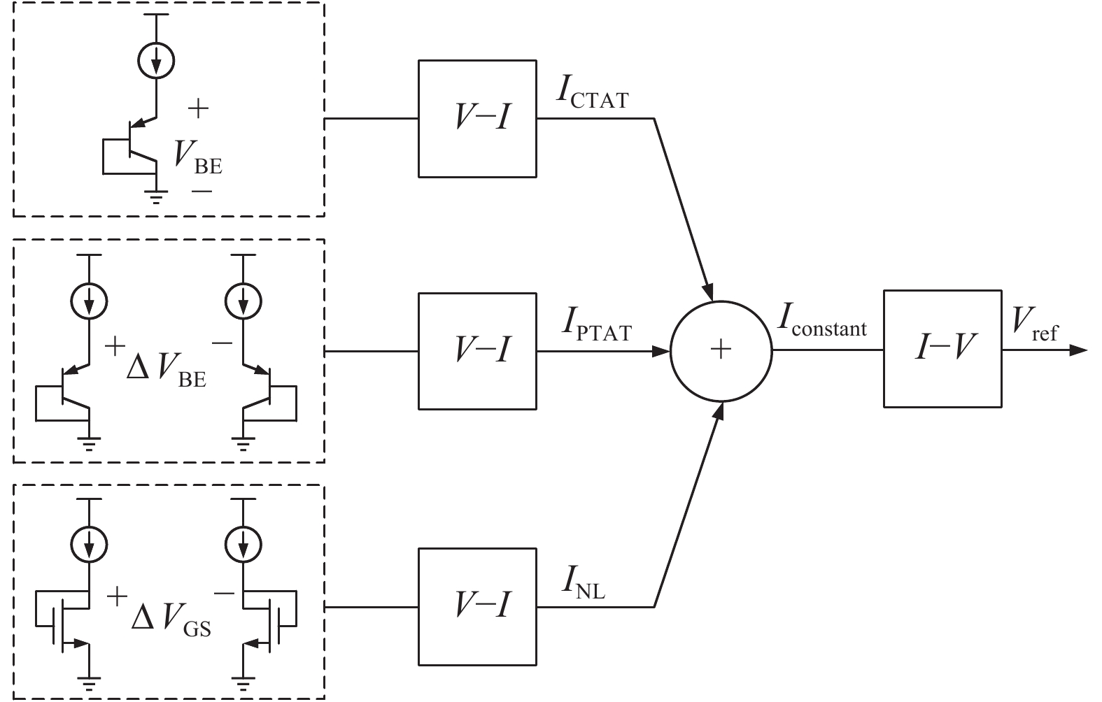
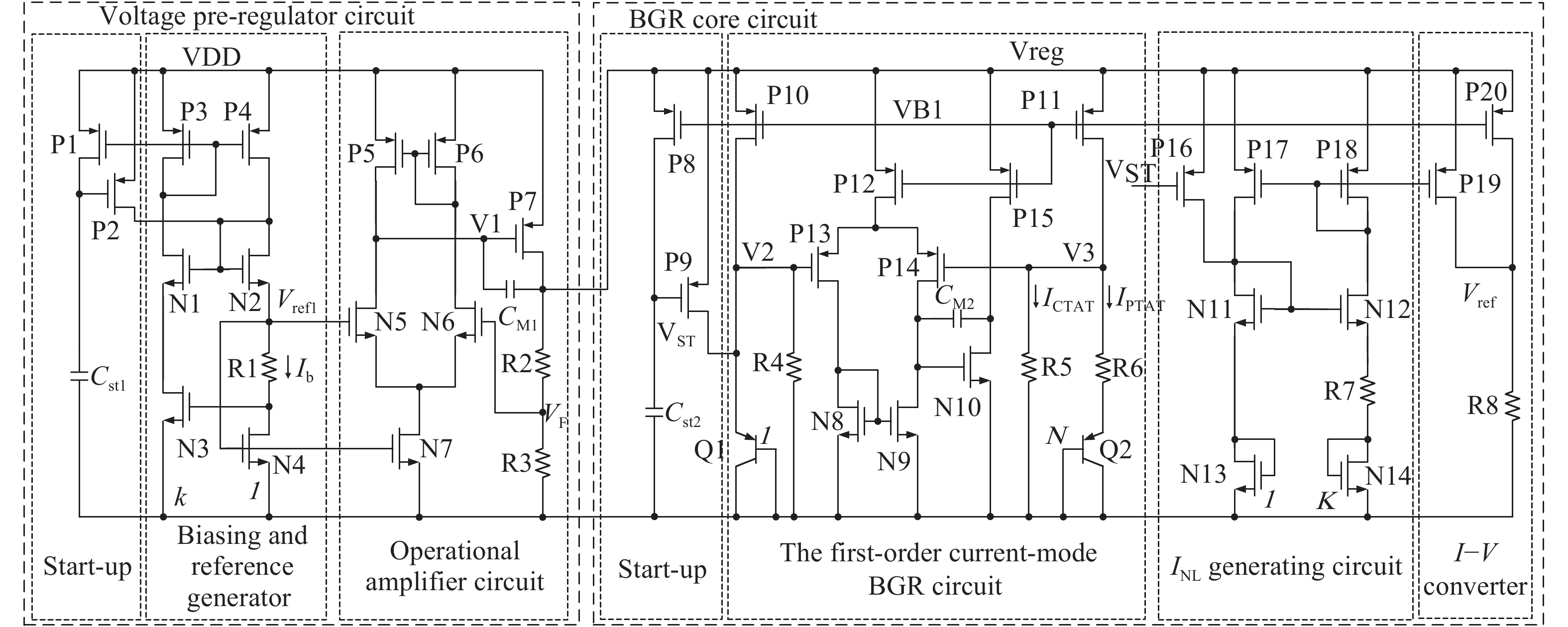
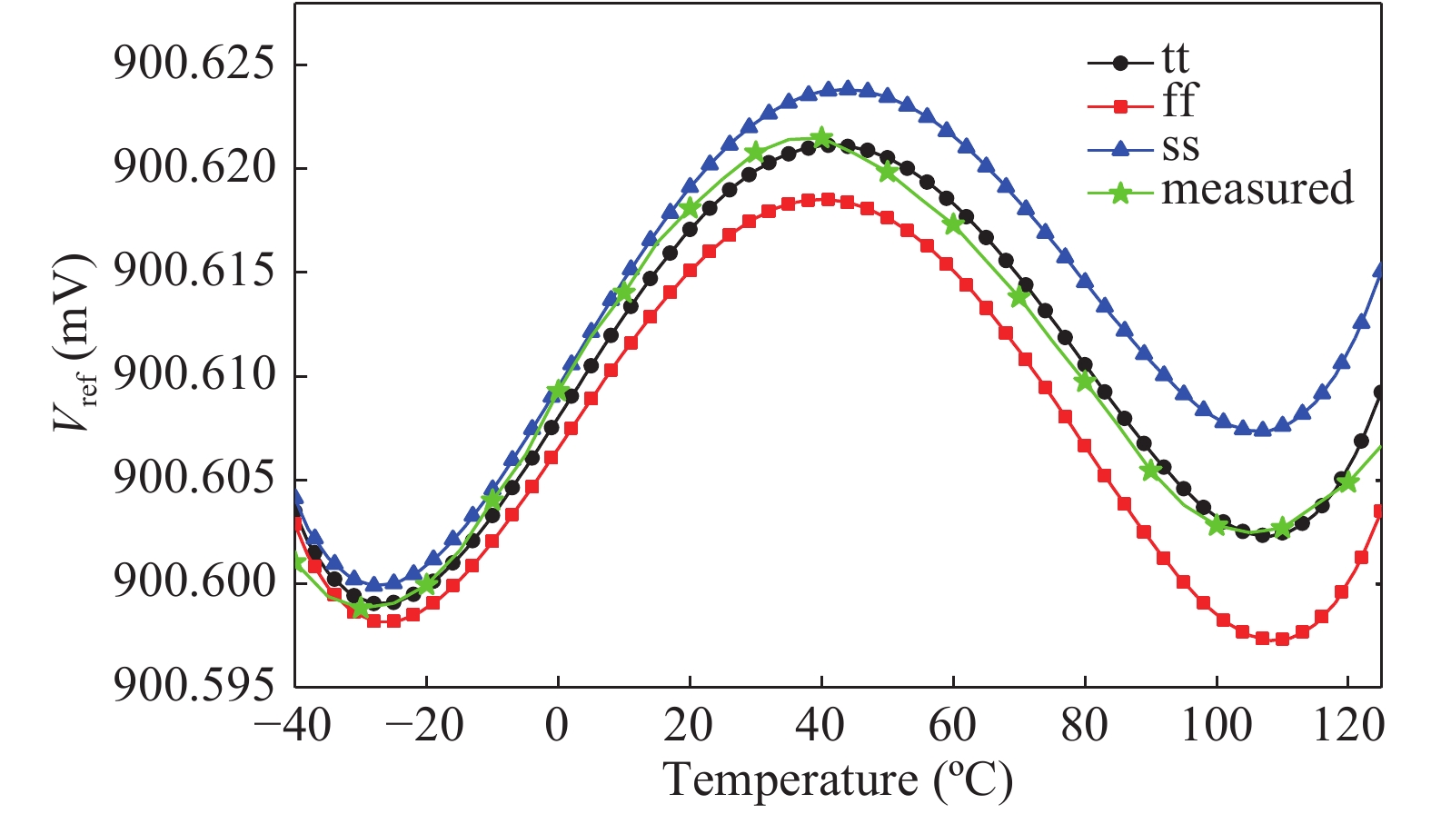
Table 1. Performance at transistor corners.
| Parameter | tt | ff | ss |
| TC (ppm/°C) | 0.147 | 0.144 | 0.159 |
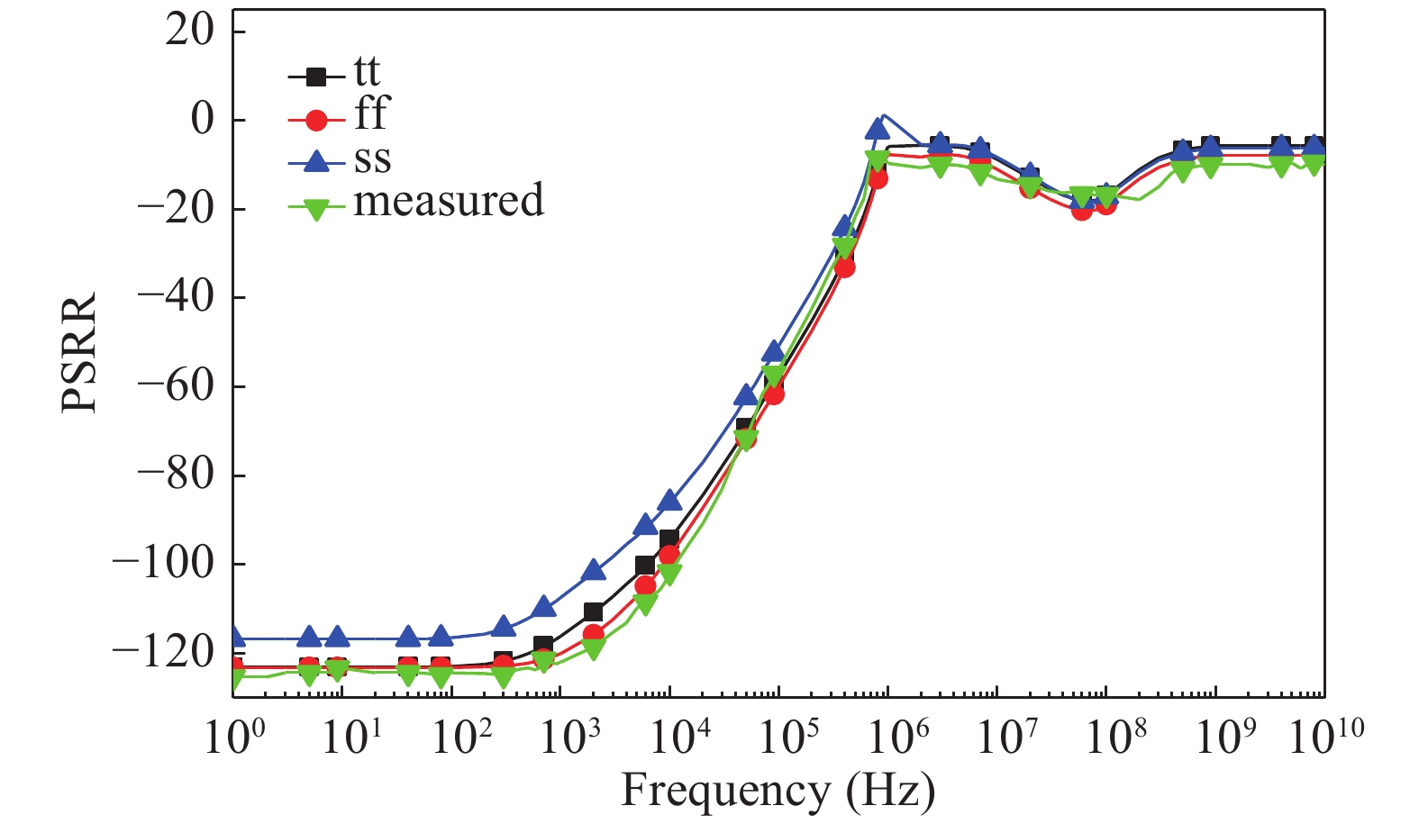
| PSRR (dB) @ DC | −125.10 | −123.24 | −116.85 |
| PSRR (dB) @ 100 kHz | −57.44 | −59.75 | −50.63 |
 DownLoad: CSV
Table 2. Comparison with other published results.
| Parameter | Ref. [11] | Ref. [12] | Ref. [13] | Ref. [14] | Ref. [15] | Ref. [16] | Ref. [17] | Ref. [18] | Ref. [19] | This work |
| Supply voltage (V) | 1.3–1.8 | 1.2–1.8 | 1.3–2.6 | 1.8–3.5 | 1.2 | 1.3–1.8 | 1.2 | 3.6 | 5 | 5 |
| Ref. voltage (V) | 1.238 | 1.09 | 1.1402 | 1.25 | 0.735 | 0.547 | 0.767 | 1.23 | 1.2937 | 0.9006 |
| Temp. range (°C) | 0–110 | −40 to 120 | −55 to 125 | −20 to 80 | −40 to 120 | −40 to 140 | −40 to 120 | −40 to 130 | −40 to 125 | −40 to 125 |
| Measured TC (ppm/°C) | 26 | 147 | 4.1 | 5.5 | 4.2 | 1.67 | 3.4~6.9 | 11.8 | 4.1 | 0.19 |
| Line regulation (%/V) | 0.08 | N/A | 0.03 | 0.045 | N/A | 0.08 | 0.054 | N/A | 0.0137 | 0.017 |
| PSRR (dB) | −46@
100 kHz |
−62@
100 kHz |
−54@
100 kHz |
N/A | −30@
100 kHz |
N/A | −40@
100 kHz |
−31.8@
10 Hz |
−81.72@
DC |
−56@
100 kHz, –123@DC |
| Technology | 0.18 µm
CMOS |
0.18 µm
CMOS |
0.18 µm
CMOS |
0.18 µm
CMOS |
0.13 µm
CMOS |
0.18 µm
CMOS |
0.18 µm
CMOS |
0.5 µm
CMOS |
0.5 µm
CMOS |
0.5 µm
CMOS |
DownLoad: CSV
| [1] |
Song B S, Gray P R. A precision curvature-compensated CMOS bandgap reference. IEEE J Solid-State Circuits, 1983, 18(6): 634 doi: 10.1109/JSSC.1983.1052013
|
| [2] |
Vogler B, Rosberg M, Herzer R. A fully integrated 600 V SOI half bridge IGBT gate driver IC. 51th IWK, Internationales Wissenschaftliches Kolloquium, 2006
|
| [3] |
Rincon-Mora G, Allen P E. A 1.1-V current-mode and piecewise-linear curvature-corrected bandgap reference. IEEE J Solid-State Circuits, 1998, 33(10): 1551 doi: 10.1109/4.720402
|
| [4] |
Huang Y, Cheung C, Najafizadeh L. A multi-piecewise curvature-corrected technique for bandgap reference circuits. 2013 IEEE 56th International Midwest Symposium on Circuits and Systems (MWSCAS), 2013: 305
|
| [5] |
Wang R, Lu W, Zhao M, et al. A 2.1-ppm/°C current-mode CMOS bandgap reference with piecewise curvature compensation. 2017 IEEE International Symposium on Circuits and Systems (ISCAS), 2017: 1
|
| [6] |
Abbasi M U, Raikos G, Saraswat R, et al. A high PSRR, ultra-low power 1.2 V curvature corrected bandgap reference for wearable EEG application. 2015 IEEE 13th International New Circuits and Systems Conference (NEWCAS), Grenoble, 2015: 1
|
| [7] |
Leung K N, Mok P K T, Leung C Y. A 2-V 23-μA 5.3-ppm/°C curvature-compensated CMOS bandgap voltage reference. IEEE J Solid-State Circuits, 2003, 38(3): 561 doi: 10.1109/JSSC.2002.808328
|
| [8] |
Zhou Z K, Yue S, Zhi H, et al. A 1.6-V 25-μA 5-ppm/°C curvature-compensated bandgap reference. IEEE Trans Circuits Syst I, 2012, 59(4): 677 doi: 10.1109/TCSI.2011.2169732
|
| [9] |
Tsividis Y P. Accurate analysis of temperature effects in IC–VBE characteristics with application to bandgap reference sources. IEEE J Solid-State Circuits, 1980, 15(6): 1076 doi: 10.1109/JSSC.1980.1051519
|
| [10] |
Palumbo G. Voltage references: from diodes to precision high-order bandgap circuits. IEEE Circuits Devices Mag, 2002, 18(5): 45 doi: 10.1109/MCD.2002.1035357
|
| [11] |
Ji Y, Jeon C, Son H, et al. 5.8 A 9.3 nW all-in-one bandgap voltage and current reference circuit. IEEE International Solid-State Circuits Conference (ISSCC), 2017: 100
|
| [12] |
Osaki Y, Hirose T, Kuroki N et al. 1.2-V supply, 100-nW, 1.09-V bandgap and 0.7-V supply, 52.5-nW, 0.55-V subbandgap reference circuits for nanowatt CMOLSIs S. IEEE J Solid-State Circuits, 2013, 48(6): 1530 doi: 10.1109/JSSC.2013.2252523
|
| [13] |
Wang B, Law M K, Bermak A. A precision CMOS voltage reference exploiting silicon bandgap narrowing effect. IEEE Trans Electron Devices, 2015, 62(7): 2128 doi: 10.1109/TED.2015.2434495
|
| [14] |
Lin C, Chen H, Xu W, et al. A novel high-precision bandgap reference with differential common-gate structure. IEEE 9th International Conference on Anti-counterfeiting, Security, and Identification (ASID), Xiamen, 2015: 47
|
| [15] |
Duan Q, Roh J. A 1.2-V 4.2-ppm/°C high-order curvature-compensated CMOS bandgap reference. IEEE Trans Circuits Syst I, 2015, 62(3): 662 doi: 10.1109/TCSI.2014.2374832
|
| [16] |
Chen H M, Lee C C, Jheng S H, et al. A sub-1 ppm/°C precision bandgap reference with adjusted-temperature-curvature compensation. IEEE Trans Circuits Syst I, 2017, 64(6): 1308 doi: 10.1109/TCSI.2017.2658186
|
| [17] |
Ma B, Yu F. A novel 1.2-V 4.5-ppm/°C curvature-compensated CMOS bandgap reference. IEEE Trans Circuits Syst I, 2014, 61(4): 1026 doi: 10.1109/TCSI.2013.2286032
|
| [18] |
Ming X, Ma Y Q, Zhou Z K, et al. A high-precision compensated CMOS bandgap voltage reference without resistors. IEEE Trans Circuits Syst II, 2010, 57(10): 767 doi: 10.1109/TCSII.2010.2067770
|
| [19] |
Lv J, Wei L, Ang S S. A new curvature-compensated, high-PSRR CMOS bandgap reference. Analog Integrated Circuits and Signal Processing, 2015, 82(3): 675 doi: 10.1007/s10470-015-0494-2
|


Article views: 9874 Times PDF downloads: 600 Times Cited by: 0 Times
Received: 12 January 2018 Revised: 01 March 2018 Online: Accepted Manuscript: 23 April 2018Uncorrected proof: 25 April 2018Published: 01 September 2018
| Citation: |
Jing Leng, Yangyang Lu, Yunwu Zhang, Huan Xu, Kongsheng Hu, Zhicheng Yu, Weifeng Sun, Jing Zhu. A 0.19 ppm/°C bandgap reference circuit with high-PSRR[J]. Journal of Semiconductors, 2018, 39(9): 095002. doi: 10.1088/1674-4926/39/9/095002
****
J Leng, Y Y Lu, Y W Zhang, H Xu, K S Hu, Z C Yu, W F Sun, J Zhu, A 0.19 ppm/°C bandgap reference circuit with high-PSRR[J]. J. Semicond., 2018, 39(9): 095002. doi: 10.1088/1674-4926/39/9/095002.

|
| [1] |
Song B S, Gray P R. A precision curvature-compensated CMOS bandgap reference. IEEE J Solid-State Circuits, 1983, 18(6): 634 doi: 10.1109/JSSC.1983.1052013
|
| [2] |
Vogler B, Rosberg M, Herzer R. A fully integrated 600 V SOI half bridge IGBT gate driver IC. 51th IWK, Internationales Wissenschaftliches Kolloquium, 2006
|
| [3] |
Rincon-Mora G, Allen P E. A 1.1-V current-mode and piecewise-linear curvature-corrected bandgap reference. IEEE J Solid-State Circuits, 1998, 33(10): 1551 doi: 10.1109/4.720402
|
| [4] |
Huang Y, Cheung C, Najafizadeh L. A multi-piecewise curvature-corrected technique for bandgap reference circuits. 2013 IEEE 56th International Midwest Symposium on Circuits and Systems (MWSCAS), 2013: 305
|
| [5] |
Wang R, Lu W, Zhao M, et al. A 2.1-ppm/°C current-mode CMOS bandgap reference with piecewise curvature compensation. 2017 IEEE International Symposium on Circuits and Systems (ISCAS), 2017: 1
|
| [6] |
Abbasi M U, Raikos G, Saraswat R, et al. A high PSRR, ultra-low power 1.2 V curvature corrected bandgap reference for wearable EEG application. 2015 IEEE 13th International New Circuits and Systems Conference (NEWCAS), Grenoble, 2015: 1
|
| [7] |
Leung K N, Mok P K T, Leung C Y. A 2-V 23-μA 5.3-ppm/°C curvature-compensated CMOS bandgap voltage reference. IEEE J Solid-State Circuits, 2003, 38(3): 561 doi: 10.1109/JSSC.2002.808328
|
| [8] |
Zhou Z K, Yue S, Zhi H, et al. A 1.6-V 25-μA 5-ppm/°C curvature-compensated bandgap reference. IEEE Trans Circuits Syst I, 2012, 59(4): 677 doi: 10.1109/TCSI.2011.2169732
|
| [9] |
Tsividis Y P. Accurate analysis of temperature effects in IC–VBE characteristics with application to bandgap reference sources. IEEE J Solid-State Circuits, 1980, 15(6): 1076 doi: 10.1109/JSSC.1980.1051519
|
| [10] |
Palumbo G. Voltage references: from diodes to precision high-order bandgap circuits. IEEE Circuits Devices Mag, 2002, 18(5): 45 doi: 10.1109/MCD.2002.1035357
|
| [11] |
Ji Y, Jeon C, Son H, et al. 5.8 A 9.3 nW all-in-one bandgap voltage and current reference circuit. IEEE International Solid-State Circuits Conference (ISSCC), 2017: 100
|
| [12] |
Osaki Y, Hirose T, Kuroki N et al. 1.2-V supply, 100-nW, 1.09-V bandgap and 0.7-V supply, 52.5-nW, 0.55-V subbandgap reference circuits for nanowatt CMOLSIs S. IEEE J Solid-State Circuits, 2013, 48(6): 1530 doi: 10.1109/JSSC.2013.2252523
|
| [13] |
Wang B, Law M K, Bermak A. A precision CMOS voltage reference exploiting silicon bandgap narrowing effect. IEEE Trans Electron Devices, 2015, 62(7): 2128 doi: 10.1109/TED.2015.2434495
|
| [14] |
Lin C, Chen H, Xu W, et al. A novel high-precision bandgap reference with differential common-gate structure. IEEE 9th International Conference on Anti-counterfeiting, Security, and Identification (ASID), Xiamen, 2015: 47
|
| [15] |
Duan Q, Roh J. A 1.2-V 4.2-ppm/°C high-order curvature-compensated CMOS bandgap reference. IEEE Trans Circuits Syst I, 2015, 62(3): 662 doi: 10.1109/TCSI.2014.2374832
|
| [16] |
Chen H M, Lee C C, Jheng S H, et al. A sub-1 ppm/°C precision bandgap reference with adjusted-temperature-curvature compensation. IEEE Trans Circuits Syst I, 2017, 64(6): 1308 doi: 10.1109/TCSI.2017.2658186
|
| [17] |
Ma B, Yu F. A novel 1.2-V 4.5-ppm/°C curvature-compensated CMOS bandgap reference. IEEE Trans Circuits Syst I, 2014, 61(4): 1026 doi: 10.1109/TCSI.2013.2286032
|
| [18] |
Ming X, Ma Y Q, Zhou Z K, et al. A high-precision compensated CMOS bandgap voltage reference without resistors. IEEE Trans Circuits Syst II, 2010, 57(10): 767 doi: 10.1109/TCSII.2010.2067770
|
| [19] |
Lv J, Wei L, Ang S S. A new curvature-compensated, high-PSRR CMOS bandgap reference. Analog Integrated Circuits and Signal Processing, 2015, 82(3): 675 doi: 10.1007/s10470-015-0494-2
|

 WeChat ID
Journal of Semiconductors © 2017 All Rights Reserved 京ICP备05085259号-2