| [1] |
Tong Q Y, Gösele U. Semiconductor wafer bonding, science and technology. John Wiley & Sons, 1999, 204
|
| [2] |
Palit S, Kirch J, Huang M, et al. Facet-embedded thin-film III–V edge-emitting lasers integrated with SU-8 waveguides on silicon. Opt Lett, 2010, 35(20), 3474 doi: 10.1364/OL.35.003474 |
| [3] |
Palit S, Kirch J, Tsvid G, et al. Low-threshold thin-film III–V lasers bonded to silicon with front and back side defined features. Opt Lett, 2009, 34(18), 2802 doi: 10.1364/OL.34.002802 |
| [4] |
Bogdanov M V, Bulashevich K A, Khokhlev O V, et al. Current crowding effect on light extraction efficiency of thin-film LEDs. Phys Stat Solidi C, 2010, 7(7/8), 2124 doi: 10.1002/pssc.200983415 |
| [5] |
Wierer J J Jr, David A, Megens M M. III-nitride photonic-crystal light-emitting diodes with high extraction efficiency. Nat Photonics, 2009, 3, 163 doi: 10.1038/nphoton.2009.21 |
| [6] |
Pouladi S, Rathi M, Khatiwada D, et al. High-efficiency flexible III–V photovoltaic solar cells based on single-crystal-like thin films directly grown on metallic tapes. Prog Photovolt Res Appl, 2019, 27, 30 doi: 10.1002/pip.3070 |
| [7] |
Tanabe K. A review of ultrahigh efficiency III–V semiconductor compound solar cells: multijunction tandem, lower dimensional. photonic up/down conversion and plasmonic nanometallic structures. Energy, 2009, 2, 504 doi: 10.3390/en20300695 |
| [8] |
Yokohama M, Yasuda T, Takagi H, et al. Thin body III–V semiconductor-on-insulator metal–oxide–semiconductor field-effect transistors on Si fabicated using direct wafer bonding. Appl Phys Express, 2009, 2, 124501 doi: 10.1143/APEX.2.124501 |
| [9] |
Ye P D. Main determinants for III–V metal–oxide–semiconductor field-effect transistors. J Vac Sci Technol A, 2008, 26(4), 697 doi: 10.1116/1.2905246 |
| [10] |
Dubrovskii V G. Theory of VLS growth of compound semiconductors, semiconductors and semimetals. Chapter 1. Elsevier Inc, 2015, 93
|
| [11] |
Bolkhovityanov Y B, Pchelyakov O P. GaAs epitaxy on Si substrates: modern status of research and engineering. Phys Usp, 2008, 51(5), 437 doi: 10.1070/PU2008v051n05ABEH006529 |
| [12] |
Wang T, Liu H, Lee A, et al. 1.3- μm InAs/GaAs quantum-dot lasers monolithically grown on Si substrates. Opt Express, 2011, 19(12), 11381 doi: 10.1364/OE.19.011381 |
| [13] |
Chang E Y, Yang T H, Luo G, et al. A GeSi-buffer structure for growth of high-quality GaAs epitaxial layers on a Si substrate. J Electron Mater, 2005, 34(1), 23 doi: 10.1007/s11664-005-0175-5 |
| [14] |
Fitzgerald E A, Xie Y H, Green M L, et al. Totally relaxed Ge xSi 1– x layers with low threading dislocation densities grown on Si substrates. Appl Phys Lett, 1991, 59, 811 doi: 10.1063/1.105351 |
| [15] |
Dixit V K, Ganguli T, Sharma T K, et al. Studies on MOVPE growth of GaP epitaxial layer on Si (001) substrate and effects of annealing. J Cryst Growth, 2006, 293(1), 5 doi: 10.1016/j.jcrysgro.2006.03.060 |
| [16] |
Komatsu Y, Hosotani K, Fuyuki T, et al. Heteroepitaxial growth of InGaP on Si with InGaP/GaP step-graded buffer layers. Jpn J Appl Phys, 1997, 36, 5425 doi: 10.1143/JJAP.36.5425 |
| [17] |
Tsuji T, Yonezu H, Ohshima N. Selective epitaxial growth of GaAs on Si with strained short-period superlattices by molecular beam epitaxy under atomic hydrogen irradiation. J Vac Sci Technol B, 2004, 22(3), 1428 doi: 10.1116/1.1736634 |
| [18] |
Gösele U, Bluhm Y, Kastner G, et al. Fundamental issues in wafer bonding. J Vac Sci Technol A, 1999, 17(4), 1145 doi: 10.1116/1.581788 |
| [19] |
Mårtensson T, Svensson C P T, Wacaser B A, et al. Epitaxial III–V nanowires on silicon. Nano Lett, 2004, 4(10), 1987 doi: 10.1021/nl0487267 |
| [20] |
Treu J, Stettner T, Watzinger M, et al. Lattice-matched InGaAs−InAlAs core−shell nanowires with improved luminescence and photoresponse properties. Nano Lett, 2015, 15(5), 3533 doi: 10.1021/acs.nanolett.5b00979 |
| [21] |
Shin J C, Lee A, Mohseni P K, et al. Wafer-scale production of uniform InAs yP 1– y nanowire array on silicon for heterogeneous integration. ACS Nano, 2013, 7(6), 5463 doi: 10.1021/nn4014774 |
| [22] |
Wu J, Li Y, Kubota J, et al. Wafer-scale fabrication of self-catalyzed 1.7 eV GaAsP core−shell nanowire photocathode on silicon substrates. Nano Lett, 2014, 14(4), 2013 doi: 10.1021/nl500170m |
| [23] |
Saxena D, Jiang N, Yuan X, et al. Design and room-temperature operation of GaAs/AlGaAs multiple quantum well nanowire lasers. Nano Lett, 2016, 16(8), 5080 doi: 10.1021/acs.nanolett.6b01973 |
| [24] |
Stettner T, Zimmermann P, Loitsch B, et al. Coaxial GaAs–AlGaAs core-multishell nanowire lasers with epitaxial gain control. Appl Phys Lett, 2016, 108, 011108 doi: 10.1063/1.4939549 |
| [25] |
Tomioka K, Motohisa J, Hara S, et al. GaAs/AlGaAs core multishell nanowire-based light-emitting diodes on Si. Nano Lett, 2010, 10(5), 1639 doi: 10.1021/nl9041774 |
| [26] |
Svensson C P T, Mårtensson T, Trägårdh J, et al. Monolithic GaAs/InGaP nanowire light emitting diodes on silicon. Nanotechnology, 2008, 19, 305201 doi: 10.1088/0957-4484/19/30/305201 |
| [27] |
Huh J, Kim D C, Munshi A M, et al. Low frequency noise in single GaAsSb nanowires with self-induced compositional gradients. Nanotechnology, 2016, 27, 385703 doi: 10.1088/0957-4484/27/38/385703 |
| [28] |
Sharma M, Ahmad E, Dev D, et al. Improved performance of GaAsSb/AlGaAs nanowire ensemble Schottky barrier based photodetector via in situ annealing. Nanotechnology, 2019, 30, 034005 doi: 10.1088/1361-6528/aae148 |
| [29] |
Ren D, Dheeraj D L, Jin C, et al. New insights into the origins of Sb-induced effects on self-catalyzed GaAsSb nanowire arrays. Nano Lett, 2016, 16(2), 1201 doi: 10.1021/acs.nanolett.5b04503 |
| [30] |
Sourribes M J L, Isakov I, Panfilova M, et al. Mobility enhancement by sb-mediated minimisation of stacking fault density in InAs nanowires grown on silicon. Nano Lett, 2014, 14(3), 1643 doi: 10.1021/nl5001554 |
| [31] |
Tomioka K, Yoshimura M, Fukui T. A III–V nanowire channel on silicon for high-performance vertical transistors. Nature, 2012, 488, 189 doi: 10.1038/nature11293 |
| [32] |
Hou J J, Han N, Wang F, et al. Synthesis and characterizations of ternary ingaas nanowires by a two-step growth method for high-performance electronic devices. ACS Nano, 2012, 6(4), 3624 doi: 10.1021/nn300966j |
| [33] |
Bengoechea-Encabo A, Barbagini F, Fernandez-Garrido S, et al. Understanding the selective area growth of GaN nanocolumns by MBE using Ti nanomasks. J Cryst Growth, 2011, 325(1), 89 doi: 10.1016/j.jcrysgro.2011.04.035 |
| [34] |
Ji X, Yang X, Du W, et al. Selective-area MOCVD growth and carrier-transport-type control of InAs(Sb)/GaSb core–shell nanowires. Nano Lett, 2016, 16(12), 7580 doi: 10.1021/acs.nanolett.6b03429 |
| [35] |
Tomioka K. Selective-area growth of III–V nanowires and their applications. J Mater Res, 2011, 26(17), 2127 doi: 10.1557/jmr.2011.103 |
| [36] |
Tomioka K, Tanaka T, Hara S, et al. III–V nanowires on Si substrate: selective-area growth and device applications. IEEE J Sel Top Quantum Electron, 2011, 17(4), 1112 doi: 10.1109/JSTQE.2010.2068280 |
| [37] |
Yamano K, Kishino K. Selective area growth of InGaN-based nanocolumn LED crystals on AlN/Si substrates useful for integrated μ-LED fabrication. Appl Phys Lett, 2018, 112(9), 091105 doi: 10.1063/1.5022298 |
| [38] |
Kohen D, Tileli V, Cayron C, et al. Al catalyzed growth of silicon nanowires and subsequent in situ dry etching of the catalyst for photovoltaic application. Phys Status Solidi A, 2011, 208(11), 2676 doi: 10.1002/pssa.201127072 |
| [39] |
Wagner R S, Ellis W C. Vapor-liquid-solid mechanism of single-crystal growth. Appl Phys Lett, 1964, 4(5), 89 doi: 10.1063/1.1753975 |
| [40] |
Messing M E, Hillerich K, Johansson J, et al. The use of gold for fabrication of nanowire structures. Gold Bulletin, 2009, 42(3), 172 doi: 10.1007/BF03214931 |
| [41] |
|
| [42] |
Li N, Tan T Y, Gösele U. Transition region width of nanowire hetero- and pn-junctions grown using vapor–liquid–solid processes. Appl Phys A, 2008, 90, 591 doi: 10.1007/s00339-007-4376-z |
| [43] |
Sarkar K, Palit M, Banerji P, et al. Silver catalyzed growth of In xGa 1– xAs nanowires on Si (001) by metal–organic chemical vapour deposition. CrystEngComm, 2015, 17, 8519 doi: 10.1039/C5CE01565K |
| [44] |
Colombo C, Spirkoska D, Frimmer M, et al. Ga-assisted catalyst-free growth mechanism of GaAs nanowires by molecular beam epitaxy. Phys Rev B, 2008, 77, 155326 doi: 10.1103/PhysRevB.77.155326 |
| [45] |
Ghalamestani S G, Ek M, Ghasemi M, et al. Morphology and composition controlled Ga xIn 1– xSb nanowires: understanding ternary antimonide growth. Nanoscale, 2014, 6, 1086 doi: 10.1039/C3NR05079C |
| [46] |
Berg A, Lenrick F, Vainorius N, et al. Growth parameter design for homogeneous material composition in ternary Ga xIn 1– xP nanowires. Nanotechnology, 2015, 26, 435601 doi: 10.1088/0957-4484/26/43/435601 |
| [47] |
Dick K A, Bolinsson J, Borg B M, et al. Controlling the abruptness of axial heterojunctions in III–V nanowires: beyond the reservoir effect. Nano Lett, 2012, 12(6), 3200 doi: 10.1021/nl301185x |
| [48] |
Motohisa J, Noborisaka J, Hara S, et al. Catalyst-free growth of semiconductor nanowires by selective area MOVPE. AIP Conference Proceedings, 2005, 772, 877 doi: 10.1063/1.1994386 |
| [49] |
Koblmuüller G, Abstreiter G. Growth and properties of InGaAs nanowires on silicon. Phys Status Solidi, 2013, 7(10), 11 doi: 10.1002/pssr.201308207 |
| [50] |
Shin J C, Choi K J, Kim D Y, et al. Characteristics of strain-induced In xGa 1– xAs nanowires grown on Si (111) substrates. Cryst Growth Des, 2012, 12, 2994 doi: 10.1021/cg300210h |
| [51] |
Glas F. Critical dimensions for the plastic relaxation of strained axial heterostructures in free-standing nanowires. Phys Rev B, 2006, 74, 121302 doi: 10.1103/PhysRevB.74.121302 |
| [52] |
Li L, Pan D, Xue Y, et al. Near full-composition-range high-quality GaAs 1– xSb x nanowires grown by molecular beam epitaxy. Nano Lett, 2017, 17(2), 622 doi: 10.1021/acs.nanolett.6b03326 |
| [53] |
|
| [54] |
|
| [55] |
de la Mata M, Magen C, Caroff P, et al. Atomic scale strain relaxation in axial semiconductor III–V nanowire heterostructures. Nano Lett, 2014, 14(11), 6614 doi: 10.1021/nl503273j |
| [56] |
Grönqvist J, Søndergaard N, Boxberg F, et al. Strain in semiconductor core/shell nanowires. J Appl Phys, 2009, 106, 053508 doi: 10.1063/1.3207838 |
| [57] |
Ferrand D, Cibert J. Strain in crystalline core-shell nanowires. Eur Phys J: Appl Phys, 2014, 67(3), 30403 doi: 10.1051/epjap/2014140156 |
| [58] |
Gagliano L, Albani M, Verheijen M A, et al. Twofold origin of strain-induced bending in core-shell nanowires: the GaP/InGaP case. Nanotechnology, 2018, 29(31), 315703 doi: 10.1088/1361-6528/aac417 |
| [59] |
Lewis R B, Corfdir P, Kupers H, et al. nanowires bending over backward from strain partitioning in asymmetric core-shell heterostructures. Nano Lett, 2018, 18(4), 2343 doi: 10.1021/acs.nanolett.7b05221 |
| [60] |
Kavanagh K L, Saveliev I, Blumin M, et al. Faster radial strain relaxation in InAs–GaAs core–shell heterowires. Appl Phys Lett, 2012, 111, 044301 doi: 10.1063/1.3684964 |
| [61] |
Dayeh S A, Tang W, Boioli F, et al. Direct measurement of coherency limits for strain relaxation in heteroepitaxial core/shell nanowires. Nano Lett, 2013, 13(5), 1869 doi: 10.1021/nl3022434 |
| [62] |
Gronqvist J, Sondergaard N, Boxberg F, et al. Strain in semiconductor core/shell nanowires. J Appl Phys, 2009, 106, 053508 doi: 10.1063/1.3207838 |
| [63] |
Biermanns A, Rieger T, Bussone G, et al. Axial strain in GaAs/InAs core–shell nanowires. Appl Phys Lett, 2013, 102, 043109 doi: 10.1063/1.4790185 |
| [64] |
Zeng H, Yu X, Fonseka H A, et al. Hybrid III–V/IV nanowires: high- quality Ge shell epitaxy on GaAs cores. Nano Lett, 2018, 18(10), 6397 doi: 10.1021/acs.nanolett.8b02760 |
| [65] |
Tietjen J J, Amick J A. The preparation and properties of vapour-deposited epitaxial GaAs 1– xP x using arsine and phosphine. J Electrochem Soc, 1966, 113, 724 doi: 10.1149/1.2424100 |
| [66] |
Priante G, Patriarche G, Oehler F, et al. Abrupt GaP/GaAs interfaces in self-catalyzed nanowires. Nano Lett, 2015, 15(9), 6036 doi: 10.1021/acs.nanolett.5b02224 |
| [67] |
Halder N N, Kelrich A, Cohen S, et al. Pure wurtzite GaP nanowires grown on zincblende GaP substrates by selective area vapor liquid solid epitaxy. Nanotechnology, 2017, 28, 465603 doi: 10.1088/1361-6528/aa8b60 |
| [68] |
Im H S, Jung C S, Park K, et al. Band gap tuning of twinned GaAsP ternary nanowires. J Phys Chem C, 2014, 118(8), 4546 doi: 10.1021/jp500458j |
| [69] |
Zhang Y, Aagesen M, Holm J V, et al. Self-catalyzed GaAsP nanowires grown on silicon substrates by solid-source molecular beam epitaxy. Nano Lett, 2013, 13(8), 3897 doi: 10.1021/nl401981u |
| [70] |
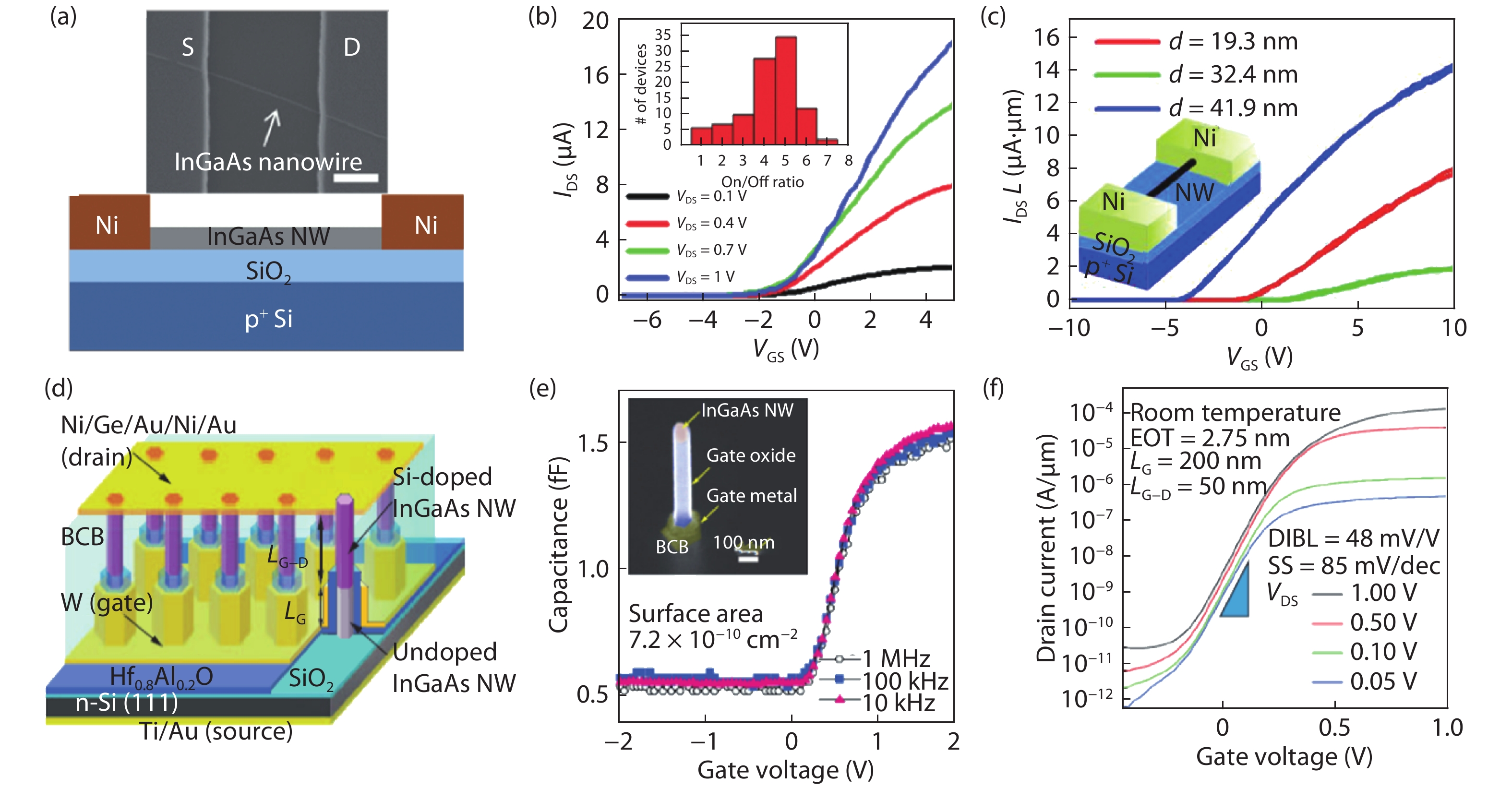
Zhang Y, Wu J, Aagesen M, et al. Self-catalyzed ternary core-shell GaAsP nanowire arrays grown on patterned Si substrates by molecular beam epitaxy. Nano Lett, 2014, 14(8), 4542 doi: 10.1021/nl501565b |
| [71] |
Wu J, Ramsay A, Sanchez A M, et al. Defect-free self-catalyzed GaAs/GaAsP nanowire quantum dots grown on silicon substrate. Nano Lett, 2016, 16(1), 504 doi: 10.1021/acs.nanolett.5b04142 |
| [72] |
Isako Iv, Panfilova M, Sourribes M J L, et al. InAs 1– xP x nanowires grown by catalyst-free molecular-beam epitaxy. Nanotechnology, 2013, 24(8), 085707 doi: 10.1088/0957-4484/24/8/085707 |
| [73] |
Lee J H, Pin M W, Choi S J, et al. Electromechanical properties and spontaneous response of the current in inasp nanowires. Nano Lett, 2016, 16(11), 6738 doi: 10.1021/acs.nanolett.6b02155 |
| [74] |
Persson A I, Björk M T, Jeppesen S, et al. InAs 1– xP x nanowires for device engineering. Nano Lett, 2006, 6(3), 403 doi: 10.1021/nl052181e |
| [75] |
Trägårdh J, Persson A I, Wagner J B, et al. Measurements of the band gap of wurtzite InAs 1– xP x nanowires using photocurrent spectroscopy. J Appl Phys, 2007, 101(12), 123701 doi: 10.1063/1.2745289 |
| [76] |
Tchernycheva M, Cirlin G E, Patriarche G, et al. Growth and characterization of InP nanowires with InAsP insertions. Nano Lett, 2007, 7(6), 1500 doi: 10.1021/nl070228l |
| [77] |
Cirlin G E, Tchernycheva M, Patriarche G, et al. Effect of postgrowth heat treatment on the structural and optical properties of InP/InAsP/InP nanowires. Semiconductors, 2012, 46(2), 175 doi: 10.1134/S1063782612020224 |
| [78] |
Ma L, Zhang X, Li H, et al. Bandgap-engineered GaAsSb alloy nanowires for near-infrared photodetection at 1.31 μm. Semicond Sci Technol, 2015, 30(10), 105033 doi: 10.1088/0268-1242/30/10/105033 |
| [79] |
Huh J, Yun H, Kim D C, et al. Rectifying single GaAsSb nanowire devices based on self-induced compositional gradients. Nano Lett, 2015, 15(6), 3709 doi: 10.1021/acs.nanolett.5b00089 |
| [80] |
Ren D, Huh J, Dheeraj D L, et al. Influence of pitch on the morphology and luminescence properties of self-catalyzed GaAsSb nanowire arrays. Appl Phys Lett, 2016, 109, 243102 doi: 10.1063/1.4971984 |
| [81] |
Yu X, Li L, Wang H, et al. Two-step fabrication of self-catalyzed Ga-based semiconductor nanowires on Si by molecular-beam epitaxy. Nanoscale, 2016, 8, 10615 doi: 10.1039/C5NR07830J |
| [82] |
Ahmad E, Karim M R, Hafiz S B, et al. A two-step growth pathway for high Sb incorporation in GaAsSb nanowires in the telecommunication wavelength range. Sci Rep, 2017, 7, 10111 doi: 10.1038/s41598-017-09280-4 |
| [83] |
Sharma M, Karim M R, Kasanaboina P, et al. Pitch-induced bandgap tuning in self-catalyzed growth of patterned GaAsSb axial and GaAs/GaAsSb core-shell nanowires using molecular beam epitaxy. Cryst Growth Des, 2017, 17(2), 730 doi: 10.1021/acs.cgd.6b01577 |
| [84] |
Alarcon-Llado E, Conesa-Boj S, Wallart X, et al. Raman spectroscopy of self-catalyzed GaAs 1– xSb x nanowires grown on silicon. Nanotechnology, 2013, 24(40), 405707 doi: 10.1088/0957-4484/24/40/405707 |
| [85] |
Conesa-Boj S, Kriegner D, Han X, et al. Gold-free ternary III–V antimonide nanowire arrays on silicon: twin-free down to the first bilayer. Nano Lett, 2014, 14(1), 326 doi: 10.1021/nl404085a |
| [86] |
Plissard S, Dick K A. WallartS, et al Gold-free GaAs/GaAsSb heterostructure nanowires grown on silicon. Appl Phys Lett, 2010, 96, 121901 doi: 10.1063/1.3367746 |
| [87] |
Alhodaib A, Noori Y J, Carrington P J, et al. Room-temperature mid-infrared emission from faceted InAsSb multi quantum wells embedded in InAs nanowires. Nano Lett, 2018, 18(1), 235 doi: 10.1021/acs.nanolett.7b03977 |
| [88] |
Du W N, Yang X G, Wang X Y, et al. The self-seeded growth of InAsSb nanowires on silicon by metal-organic vapour phase epitaxy. J Cryst Growth, 2014, 396, 33 doi: 10.1016/j.jcrysgro.2014.03.020 |
| [89] |
|
| [90] |
Zhang Q D, Anyebe E A, Chen R, et al. Sb-induced phase control of InAsSb nanowires grown by molecular beam epitaxy. Nano Lett, 2015, 15(2), 1109 doi: 10.1021/nl5040946 |
| [91] |
Du W, Yang X, Pan H, et al. Two different growth mechanisms for Au-free InAsSb nanowires growth on Si substrate. Cryst Growth Des, 2015, 15(5), 2413 doi: 10.1021/acs.cgd.5b00201 |
| [92] |
Du W, Yang X, Pan H, et al. Controlled-direction growth of planar InAsSb nanowires on Si substrates without foreign catalysts. Nano Lett, 2016, 16(2), 877 doi: 10.1021/acs.nanolett.5b03587 |
| [93] |
Zhuang Q D, Alradhi H, Jin Z M, et al. Optically efficient InAsSb nanowires for silicon-based mid-wavelength infrared optoelectronics. Nanotechnology, 2017, 28(10), 105710 doi: 10.1088/1361-6528/aa59c5 |
| [94] |
Anyebe E A, Rajpalke M K, Veal T D, et al. Surfactant effect of antimony addition to the morphology of self-catalyzed InAs 1– xSb x nanowires. Nano Res, 2015, 8(4), 1309 doi: 10.1007/s12274-014-0621-x |
| [95] |
Thompson M D, Alhodaib A, Craig A P, et al. Low Leakage-current InAsSb nanowire photodetectors on silicon. Nano Lett, 2016, 16(1), 182 doi: 10.1021/acs.nanolett.5b03449 |
| [96] |
Cirlin G E, Reznik R R, Shtrom I V, et al. AlGaAs and AlGaAs/GaAs/AlGaAs nanowires grown by molecular beam epitaxy on silicon substrates. J Phys D, 2017, 50(48), 484003 doi: 10.1088/1361-6463/aa9169 |
| [97] |
Tambe M J, Lim S K, Smith M J, et al. Realization of defect-free epitaxial core/shell GaAs/AlGaAs nanowire heterostructures. Appl Phys Lett, 2008, 93, 151917 doi: 10.1063/1.3002299 |
| [98] |
Titova L V, Hoang T B, Jackson H E, et al. Temperature dependence of photoluminescence from single core–shell GaAs–AlGaAs nanowires. Appl Phys Lett, 2006, 89, 173126 doi: 10.1063/1.2364885 |
| [99] |
Hoang T B, Titova L V, Yarrison-Rice J M, et al. Resonant excitation and imaging of non-equilibrium exciton spins in single core-shell GaAs-AlGaAs nanowires. Nano Lett, 2007, 7(3), 588 doi: 10.1021/nl062383q |
| [100] |
Koblmuüller G, Mayer B, Stettner T, et al. GaAs-AlGaAs core-shell nanowire lasers on silicon: invited review. Semicond Sci Technol, 2017, 32, 053001 doi: 10.1088/1361-6641/aa5e45 |
| [101] |
Saxena D, Mokkapati S, Parkinson P, et al. Optically pumped room-temperature GaAs nanowire lasers. Nat Photonics, 2013, 7, 963 doi: 10.1038/nphoton.2013.303 |
| [102] |
Heiss M, Fontana Y, Gustafsson A, et al. Self-assembled quantum dots in a nanowire system for quantum photonics. Nat Mater, 2013, 12, 439 doi: 10.1038/nmat3557 |
| [103] |
Chen C, Shehata S, Fradin C R , et al. Self-directed growth of AlGaAs core-shell nanowires for visible applications. Nano Lett, 2007, 7(9), 2584 doi: 10.1021/nl070874k |
| [104] |
Wu Z H, Sun M, Mei X Y, et al. Growth and photoluminescence characteristics of AlGaAs nanowires. Appl Phys Lett, 2004, 85(4), 657 doi: 10.1063/1.1775037 |
| [105] |
Dubrovskii V G, Shtrom I V, Reznik R R, et al. Origin of spontaneous core-shell AlGaAs nanowires grown by molecular beam epitaxy. Crys Growth Des, 2016, 16(12), 7251 doi: 10.1021/acs.cgd.6b01412 |
| [106] |
Guo J, Hang H, Ding Y, et al. Growth of zinc blende GaAs/AlGaAs heterostructure nanowires on Si substrate by using AlGaAs buffer layers. J Cryst Growth, 2012, 359, 30 doi: 10.1016/j.jcrysgro.2012.07.047 |
| [107] |
Loitsch B, Winnerl J, Grimaldi G, et al. Crystal phase quantum dots in the ultrathin core of GaAs–AlGaAs core–shell nanowires. Nano Lett, 2015, 15(11), 7544 doi: 10.1021/acs.nanolett.5b03273 |
| [108] |
Dietrich C P, Fiore A, Thompson M G, et al. GaAs integrated quantum photonics: Towards compact and multi-functional quantum photonic integrated circuits. Laser Photonics Rev, 2016, 10(6), 870 doi: 10.1002/lpor.201500321 |
| [109] |
Chen R, Tran T T D, Ng K W, et al. Nanolasers grown on silicon. Nat Photonics, 2011, 5, 170 doi: 10.1038/nphoton.2010.315 |
| [110] |
Tatebayashi J, Kako S, Ho J, et al. Room-temperature lasing in a single nanowire with quantum dots. Nat Photonics, 2015, 9, 501 doi: 10.1038/nphoton.2015.111 |
| [111] |
Hou J J, Wang F, Han N, et al. Stoichiometric effect on electrical, optical and structural properties of composition-tunable In xGa 1– xAs nanowires. ACS Nano, 2012, 6(10), 9320 doi: 10.1021/nn304174g |
| [112] |
Shin J C, Kim D Y, Lee A, et al. Improving the composition uniformity of Au-catalyzed InGaAs nanowires on silicon. J Cryst Growth, 2013, 372, 15 doi: 10.1016/j.jcrysgro.2013.02.025 |
| [113] |
Shin J C, Kim K H, Hu H, et al. Monolithically grown In xGa1– xAs nanowire array on silicon tandem solar cells with high efficiency. IEEE Photonic Society 24th Annual Meeting, 2011
|
| [114] |
Shin J C, Kim K H, Yu K J, et al. In xGa 1– xAs nanowires on silicon: one-dimensional heterogeneous epitaxy, bandgap engineering, and photovoltaics. Nano Lett, 2011, 11(11), 4831 doi: 10.1021/nl202676b |
| [115] |
Treu J, Speckbacher M, Saller K, et al. Widely tunable alloy composition and crystal structure in catalyst-free InGaAs nanowire arrays grown by selective area molecular beam epitaxy. Appl Phys Lett, 2016, 108(5), 053110 doi: 10.1063/1.4941407 |
| [116] |
Morkötter S, Funk S, Liang M, et al. Role of microstructure on optical properties in high-uniformity In xGa 1– xAs nanowire arrays: Evidence of a wider wurtzite band gap. Phys Rev B, 2013, 87, 205303 doi: 10.1103/PhysRevB.87.205303 |
| [117] |
Berg A, Yazdi S, Nowzari A, et al. Radial nanowire light-emitting diodes in the (Al xGa 1– x) yIn 1– yP material system. Nano Lett, 2016, 16(1), 656 doi: 10.1021/acs.nanolett.5b04401 |
| [118] |
Kivisaari P, Berg A, Karimi M, et al. Optimization of current injection in AlGaInP core-shell nanowire light-emitting diodes. Nano Lett, 2017, 17(6), 3599 doi: 10.1021/acs.nanolett.7b00759 |
| [119] |
Li X, Shi T, Liu G, et al. Absorption enhancement of GaInP nanowires by tailoring transparent shell thicknesses and its application in III–V nanowire/Si film two-junction solar cells. Opt Express, 2015, 23(19), 25316 doi: 10.1364/OE.23.025316 |
| [120] |
Amiri S E H, Ranga P, Li D Y, et al. Growth of InGaP alloy nanowires with widely tunable bandgaps on silicon substrates. Conference on Lasers and Electro-Optics, 2017
|
| [121] |
Tatebayashi J, Lin A, Wong P S, et al. Visible light emission from self-catalyzed GaInP/GaP core-shell double heterostructure nanowires on silicon. J Appl Phys, 2010, 108, 034315 doi: 10.1063/1.3457355 |
| [122] |
Fakhr A, Haddara Y M, LaPierre R R. Dependence of InGaP nanowire morphology and structure on molecular beam epitaxy growth conditions. Nanotechnology, 2010, 21(16), 165601 doi: 10.1088/0957-4484/21/16/165601 |
| [123] |
Jacobsson D, Persson J M, Kriegner D, et al. Particle-assisted Ga xIn 1– xP nanowire growth for designed bandgap structures. Nanotechnology, 2012, 23(24), 245601 doi: 10.1088/0957-4484/23/24/245601 |
| [124] |
Berg A, Caroff P, Shahid N, et al. Growth and optical properties of In xGa 1– xP nanowires synthesized by selective-area epitaxy. Nano Res, 2017, 10(2), 672 doi: 10.1007/s12274-016-1325-1 |
| [125] |
Otnes G, Heurlin M, Zeng X L, et al. In xGa 1–xP nanowire growth dynamics strongly affected by doping using diethylzinc. Nano Lett, 2017, 17(2), 702 doi: 10.1021/acs.nanolett.6b03795 |
| [126] |
Ghalamestani S G, Ek M, Gamjipour B, et al. Demonstration of defect-free and composition tunable Ga xIn 1– xSb nanowires. Nano Lett, 2012, 12(9), 4914 doi: 10.1021/nl302497r |
| [127] |
Zhou H, Pozuelo M, Hicks R F, et al. Self-catalyzed vapour-liquid-solid growth of InP 1– xSb x nanostructures. J Cryst Growth, 2011, 319, 25 doi: 10.1016/j.jcrysgro.2011.01.036 |
| [128] |
Russell H B, Andriotis A N, Menon M, et al. Direct band gap gallium antimony phosphide (GaSb xP 1– x) alloys. Sci Rep, 2016, 6, 20822 doi: 10.1038/srep20822 |
| [129] |
Gagliano L, Kruijsse M, Schefold J D D, et al. Efficient green emission from wurtzite Al xIn 1– xP nanowires. Nano Lett, 2018, 18(6), 3543 doi: 10.1021/acs.nanolett.8b00621 |
| [130] |
Mayer B, Rudolph D, Schnell J, et al. Lasing from individual GaAs–AlGaAs core–shell nanowires up to room temperature. Nat Commun, 2013, 4, 2931 doi: 10.1038/ncomms3931 |
| [131] |
Birowosuto M D, Yokoo A, Zhang G, et al. Movable high- Q nanoresonators realized by semiconductor nanowires on a Si photonic crystal platform. Nat Mater, 2014, 13, 279 doi: 10.1038/nmat3873 |
| [132] |
Ren D, Ahtapodov L, Nilsen J S, et al. Single-mode near-infrared lasing in a GaAsSb-based nanowire superlattice at room temperature. Nano Lett, 2018, 18(4), 2304 doi: 10.1021/acs.nanolett.7b05015 |
| [133] |
Stettner T, Thurn A, Döblinger M, et al. Tuning lasing emission toward long wavelengths in GaAs-(In,Al)GaAs core-multishell nanowires. Nano Lett, 2018, 18(10), 6292 doi: 10.1021/acs.nanolett.8b02503 |
| [134] |
Kim H, Lee W J, Farrell A C, et al. Telecom-wavelength bottom-up nanobeam lasers on silicon-on-insulator. Nano Lett, 2017, 17, 5244 doi: 10.1021/acs.nanolett.7b01360 |
| [135] |
Kim H, Farrell A C, Senanayake P, et al. Monolithically integrated InGaAs nanowires on 3D structured silicon-on-insulator as a new platform for full optical links. Nano Lett, 2016, 16, 1833 doi: 10.1021/acs.nanolett.5b04883 |
| [136] |
Lee W J, Kim H, You J B, et al. Ultracompact bottom-up photonic crystal lasers on silicon-on-insulator. Sci Rep, 2017, 7, 9543 doi: 10.1038/s41598-017-10031-8 |
| [137] |
Zhang Y, Liu H. Nanowires for high-efficiency, low-cost solar photovoltaics. Crystals, 2019, 9(2), 87 doi: 10.3390/cryst9020087 |
| [138] |
Lin R, Galan S V, Sun H, et al. Tapering-induced enhancement of light extraction efficiency of nanowire deep ultraviolet LED by theoretical simulations. Photonics Res, 2018, 6(5), 457 doi: 10.1364/PRJ.6.000457 |
| [139] |
Zhang Y, Sanchez A M, Aagesen M, et al. Growth and fabrication of high-quality single nanowire devices with radial p–i–n junctions. Small, 2019, 15(3), 1803684 doi: 10.1002/smll.201803684 |
| [140] |
Holm J V, Jørgensen H I, Krogstrup P, et al. Surface-passivated GaAsP single-nanowire solar cells exceeding 10% efficiency grown on silicon. Nat Commun, 2013, 4, 1498 doi: 10.1038/ncomms2510 |
| [141] |
Hou J J, Wang F, Han N, et al. Diameter dependence of electron mobility in InGaAs nanowires. Appl Phys Lett, 2013, 102(9), 093112 doi: 10.1063/1.4794414 |
| [142] |
Kilpi O P, Svensson J, Wu J, et al. Vertical InAs/InGaAs heterostructure metal–oxide–semiconductor field-effect transistors on Si. Nano Lett, 2017, 17(10), 6006 doi: 10.1021/acs.nanolett.7b02251 |


 DownLoad: