


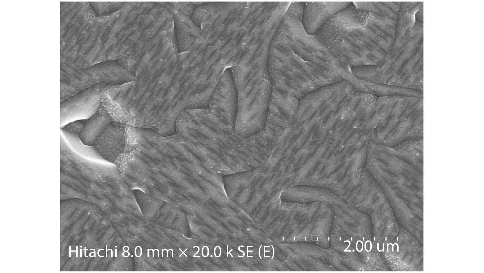
Fig. 1.
Plane view SEM image of GaAs on Ge etched by melt KOH.
REVIEWS
Wenyu Yang1, 2, 3, Yajie Li1, 2, 3, Fangyuan Meng1, 2, 3, Hongyan Yu1, 2, 3, Mengqi Wang1, 2, 3, Pengfei Wang1, 2, 3, Guangzhen Luo1, 2, 3, Xuliang Zhou1, 2, 3, and Jiaoqing Pan1, 2, 3,
Corresponding author: Xuliang Zhou, e-mail: zhouxl@semi.ac.cn; Jiaoqing Pan, e-mail: jppanl@semi.ac.cn
Abstract: Silicon-based photonic integration has attracted the interest of semiconductor scientists because it has high luminous efficiency and electron mobility. Breakthroughs have been made in silicon-based integrated lasers over the past few decades. Here we review three main methods of integration of III–V materials on Si, namely direct growth, bonding, and selective-area hetero-epitaxy. The III–V materials we introduced mainly include materials such as GaAs and InP. The lasers are mainly lasers of related communication bands. We also introduced the advantages and challenges of the three methods.
Keywords: integrated photonics, hybrid laser, silicon
| [1] |
Kim S, Yokoyama M, Taoka N, et al. Self-aligned metal source/drain InxGa1– xAs n-metal–oxide–semiconductor field-effect transistors using Ni–InGaAs Alloy. Appl Phys Lett, 2011, 98(24), 21 doi: 10.1143/APEX.4.024201
|
| [2] |
Noda H, Murai F, Kimura S. Threshold voltage controlled 0.1-μm MOSFET utilizing inversion layer as extreme shallow source/drain. International Electron Devices Meeting, 1993
|
| [3] |
Lee C G, Wang X D, Kysar J W, et al. Measurement of the elastic properties and intrinsic strength of monolayer graphene. Science, 2008, 321(5887), 385 doi: 10.1126/science.1157996
|
| [4] |
Geim A K, Novoselov K S. The rise of graphene. Nat Mater, 2009, 6, 183 doi: 10.1038/nmat1849
|
| [5] |
Coldren L A, Corzine S W, Mashanovitch M L. Diode lasers and photonic integrated circuits. Wiley, 1995
|
| [6] |
Almeida V R, Barrios C A, Panepucci R R, et al. All-optical control of light on a silicon chip. Nature, 2004, 431(7012), 1081 doi: 10.1038/nature02921
|
| [7] |
Michel J, Liu J, Kimerling L C. High-performance Ge-on-Si photodetectors. Nat Photonics, 2000, 4(8), 527 doi: 10.1038/nphoton.2010.157
|
| [8] |
Sun C, Wade M T, Lee Y, et al. Single-chip microprocessor that communicates directly using light. Nature, 2015, 528(7583), 534 doi: 10.1038/nature16454
|
| [9] |
Vlasov Y, Green W M J, Xia F J. High-throughput silicon nanophotonic wavelength-insensitive switch for on-chip optical networks. Nat Photonics, 2008, 2(4), 1 doi: 10.1038/nphoton.2008.31
|
| [10] |
Wesołowski K. Introduction to digital communication systems. Wiley, 2009
|
| [11] |
Won R, Paniccia M J. Integrating silicon photonics. Nat Photonics, 2010, 4(8), 498 doi: 10.1038/nphoton.2010.189
|
| [12] |
Andrew L, Qi J, Mingchu T, et al. Continuous-wave InAs/GaAs quantum-dot laser diodes monolithically grown on Si substrate with low threshold current densities. Opt Express, 2012, 20(20), 22181 doi: 10.1364/OE.20.022181
|
| [13] |
Bringans R D, Biegelsen D K, Swartz L. Atomic-step rearrangement on Si(100) by interaction with arsenic and the implication for GaAs-on-Si epitaxy. Phys Rev, 1991, 44(7), 3054 doi: 10.1103/PhysRevB.44.3054
|
| [14] |
Chen S, Li W, Wu J, et al. Electrically pumped continuous-wave III–V quantum dot lasers on silicon. Semiconductor Laser Conference, 2016
|
| [15] |
Mori H, Tachikawa M, Sugo M, et al. GaAs heteroepitaxy on an epitaxial Si surface with a low-temperature process. Appl Phys Lett, 1993, 63(14), 1963 doi: 10.1063/1.110615
|
| [16] |
Sakai S, Soga T, Takeyasu M, et al. Room-temperature laser operation of AlGaAs/GaAs double heterostructures fabricated on Si substrates by metalorganic chemical vapor deposition. Appl Phys Lett, 1986, 48(6), 413 doi: 10.1063/1.96515
|
| [17] |
Tang M, Chen S, Jiang W, et al. Optimisation of 1.3-μm InAs/GaAs quantum-dot lasers monolithically grown on Si substrates. Semiconductor Laser Conference, 2014
|
| [18] |
Ting S M, Fitzgerald E A. Metal-organic chemical vapor deposition of single domain GaAs on Ge/GexSi1– x/Si and Ge substrates. J Appl Phys, 2000, 87(5), 2618 doi: 10.1063/1.372227
|
| [19] |
Windhorn T H, Metze G M, Tsaur B Y, et al. AlGaAs double-heterostructure diode lasers fabricated on a monolithic GaAs/Si substrate. Appl Phys Lett, 1984, 45(4), 309 doi: 10.1063/1.95273
|
| [20] |
Takano Y, Hisaka M, Fujii N, et al. Reduction of threading dislocations by InGaAs interlayer in GaAs layers grown on Si substrates. Appl Phys Lett, 1998, 73(20), 2917 doi: 10.1063/1.122629
|
| [21] |
Asai K, Katahama H, Shiba Y. Dynamical formation process of pure edge misfit dislocations at GaAs/Si interfaces in post-annealing. J Appl Phys, 1994, 33(9A), 4843 doi: 10.1143/JJAP.33.4843
|
| [22] |
Takagi Y, Yonezu H, Hachiya Y, et al. Reduction mechanism of threading dislocation density in GaAs epilayer grown on Si substrate by high-temperature annealing. Jpn J Appl Phys, 1994, 33(6R), 3368 doi: 10.1143/JJAP.33.3368
|
| [23] |
Kohama Y, Kadota Y, Ohmachi Y. InP grown on Si substrates with GaP buffer layers by metalorganic chemical vapor deposition. Jpn J Appl Phys, 1989, 28(8), 1337 doi: 10.1143/JJAP.28.1337
|
| [24] |
Fischer R, Kopp W, Morkoc H, et al. Low threshold laser operation at room temperature in GaAs/(Al, Ga)As structures grown directly on (100)Si. Appl Phys Lett, 1986, 48(20), 1360 doi: 10.1063/1.96909
|
| [25] |
Zhou X L, Pan J Q, Liang R R, et al. Epitaxy of GaAs thin film with low defect density and smooth surface on Si substrate. J Semicond, 2014, 35, 073002 doi: 10.1088/1674-4926/35/7/073002
|
| [26] |
Li Y, Giling L J. A closer study on the self-annihilation of antiphase boundaries in GaAs epilayers. J Cryst Growth, 1996, 163(3), 203 doi: 10.1016/0022-0248(95)00975-2
|
| [27] |
Tang M, Chen S, Wu J, et al. 1.3-μm InAs/GaAs quantum-dot lasers monolithically grown on Si substrates using InAlAs/GaAs dislocation filter layers. Opt Express, 2014, 22(10), 11528 doi: 10.1364/OE.22.011528
|
| [28] |
Sugo M, Mori H, Sakai Y, et al. Stable cw operation at room temperature of a 1.5-μm wavelength multiple quantum well laser on a Si substrate. Appl Phys Lett, 1992, 60(4), 472 doi: 10.1063/1.106638
|
| [29] |
Liu H, Wang T, Qi J, et al. Long-wavelength InAs/GaAs quantum-dot laser diode monolithically grown on Ge substrate. Nat Photonics, 2011, 5(7), 416 doi: 10.1038/nphoton.2011.120
|
| [30] |
Chen S, Li W, Wu J, et al. Electrically pumped continuous-wave III–V quantum dot lasers on silicon. Nat Photonics, 2016, 10(5), 307 doi: 10.1038/nphoton.2016.21
|
| [31] |
Jinkwan K, Bongyong J, Joohang L, et al. All MBE grown InAs/GaAs quantum dot lasers on on-axis Si (001). Opt Express, 2018, 26(9), 11568 doi: 10.1364/OE.26.011568
|
| [32] |
Norman J C, Jung D, Zhang Z, et al. A review of high-performance quantum dot lasers on silicon. IEEE J Quantum Electron, 2019, 55(2), 1 doi: 10.1109/JQE.2019.2901508
|
| [33] |
Jung D, Herrick R, Norman J, et al. Impact of threading dislocation density on the lifetime of InAs quantum dot lasers on Si. Appl Phys Lett, 2018, 112(15), 153507 doi: 10.1063/1.5026147
|
| [34] |
Liu A Y, Zhang Y C, Norman J, et al. High performance continuous wave 1.3 μm quantum dot lasers on silicon. Appl Phys Lett, 2014, 104(4), 041104 doi: 10.1063/1.4863223
|
| [35] |
Zhu S, Shi B, Li Q, et al. 1.5 μm quantum-dot diode lasers directly grown on CMOS-standard (001) silicon. Appl Phys Lett, 2018, 113(22), 221103 doi: 10.1063/1.5055803
|
| [36] |
Wan Y, Qiang L, Liu A Y, et al. Sub-wavelength InAs quantum dot micro-disk lasers epitaxially grown on exact Si (001) substrates. Appl Phys Lett, 2016, 108(22), 1 doi: 10.1063/1.4952600
|
| [37] |
Norman J, Kennedy M J, Selvidge J, et al. Electrically pumped continuous wave quantum dot lasers epitaxially grown on patterned, on-axis (001) Si. Opt Express, 2017, 25(4), 3927 doi: 10.1364/OE.25.003927
|
| [38] |
Isenberg J, Warta W J. Free carrier absorption in heavily doped silicon layers. Appl Phys Lett, 2004, 84(13), 2265 doi: 10.1063/1.1690105
|
| [39] |
Krishnamoorthy A V, Chirovsky L M F, Hobson W S, et al. Vertical-cavity surface-emitting lasers flip-chip bonded to gigabit-per-second CMOS circuits. IEEE Photonics Technol Lett, 1999, 11(1), 128 doi: 10.1109/68.736418
|
| [40] |
Fang A W, Erica L, Kuo Y H, et al. A distributed feedback silicon evanescent laser. Opt Express, 2008, 16(7), 4413 doi: 10.1364/OE.16.004413
|
| [41] |
Fang A W, Hyundai P, Oded C, et al. Electrically pumped hybrid AlGaInAs-silicon evanescent laser. Opt Express, 2006, 14(20), 9203 doi: 10.1364/OE.14.009203
|
| [42] |
Fang A W, Koch B R, Jones R, et al. A distributed Bragg reflector silicon evanescent laser. IEEE Photonics Technol Lett, 2008, 20(20), 1667 doi: 10.1109/LPT.2008.2003382
|
| [43] |
Groote A D, Cardile P, Subramanian A Z, et al. Transfer-printing-based integration of single-mode waveguide-coupled III–V-on-silicon broadband light emitters. Opt Express, 2016, 24(13), 13754 doi: 10.1364/OE.24.013754
|
| [44] |
Hyundai P F, Alexander F K, Satoshi K, et al. Hybrid silicon evanescent laser fabricated with a silicon waveguide and III–V offset quantum wells. Opt Express, 2005, 13(23), 9460 doi: 10.1364/OPEX.13.009460
|
| [45] |
Justice J, Bower C, Meitl M, et al. Wafer-scale integration of group III–V lasers on silicon using transfer printing of epitaxial layers. Nat Photonics, 2012, 6(9), 612 doi: 10.1038/nphoton.2012.204
|
| [46] |
Pasquariello D, Hjort K J. Plasma-assisted InP-to-Si low temperature wafer bonding. IEEE J Sel Top Quantum Electron, 2002, 8(1), 118 doi: 10.1109/2944.991407
|
| [47] |
Keyvaninia S, Verstuyft S, Van Landschoot L, et al. Heterogeneously integrated III–V/silicon distributed feedback lasers. Opt Lett, 2013, 38(24), 5434 doi: 10.1364/OL.38.005434
|
| [48] |
Sui S, Tang M T, Yang Y, et al. Sixteen-wavelength hybrid AlGaInAs/Si microdisk laser array. IEEE J Quantum Electron, 2015, 51, 2600108 doi: 10.1109/jqe.2015.2397601
|
| [49] |
Andrijasevic D, Austerer M, Andrews A M, et al. Hybrid integration of GaAs quantum cascade lasers with Si substrates by thermocompression bonding. Appl Phys Lett, 2008, 92(5), 157 doi: 10.1063/1.2841635
|
| [50] |
Yuan L, Tao L, Yu H, et al. Hybrid InGaAsP-Si evanescent laser by selective-area metal-bonding method. IEEE Photonics Technol Lett, 2013, 25(25), 1180 doi: 10.1109/LPT.2013.2262265
|
| [51] |
Yuan L, Tao L, Chen W, et al. A buried ridge stripe structure InGaAsP-Si hybrid laser. IEEE Photonics Technol Lett, 2015, 27(4), 352 doi: 10.1109/LPT.2014.2372892
|
| [52] |
Hong T, Wang Y, Yu H Y, et al. A Selective area metal bonding method for Si photonics light sources. IEEE International Conference on Group IV Photonics, 2010
|
| [53] |
Yu H, Yuan L, Tao L, et al. 1550 nm evanescent hybrid InGaAsP-Si laser with buried ridge stripe structure. IEEE Photonics Technol Lett, 2016, 28(10), 1146 doi: 10.1109/LPT.2016.2532926
|
| [54] |
Langdo T A, Leitz C W, Currie M T, et al. High quality Ge on Si by epitaxial necking. Appl Phys Lett, 2000, 76(25), 3700 doi: 10.1063/1.126754
|
| [55] |
Li Q, Han S M, Brueck S R J, et al. Selective growth of Ge on Si(100) through vias of SiO2 nanotemplate using solid source molecular beam epitaxy. Appl Phys Lett, 2003, 83(24), 5032 doi: 10.1063/1.1632037
|
| [56] |
Matyi R J, Shichijo H, Tsai H L, et al. Patterned growth of gallium arsenide on silicon. J Vac Sci Technol B, 1988, 6(2), 699 doi: 10.1116/1.584396
|
| [57] |
Woodbridge K, Barnes P, Murray R, et al. GaAs / AlGaAs pin MQW structures grown on patterned Si substrates. J Cryst Growth, 1993, 127(1–4), 112 doi: 10.1016/0022-0248(93)90588-n
|
| [58] |
Park J S, Bai J, Curtin M, et al. Defect reduction of selective Ge epitaxy in trenches on Si(001) substrates using aspect ratio trapping. Appl Phys Lett, 2007, 90(5), 3344 doi: 10.1063/1.2435603
|
| [59] |
Li J Z, Bai J, Park J S, et al. Defect reduction of GaAs epitaxy on Si (001) using selective aspect ratio trapping. Appl Phys Lett, 2007, 91(2), 2293 doi: 10.1063/1.2756165
|
| [60] |
Li S, Zhou X, Kong X, et al. Evaluation of growth mode and optimization of growth parameters for GaAs epitaxy in V-shaped. J Cryst Growth, 2015, 426, 147 doi: 10.1016/j.jcrysgro.2015.05.033
|
| [61] |
Li S Y, Zhou X L, Kong X T, et al. Selective area growth of GaAs in V-grooved trenches on Si (001) substrates by aspect-ratio. Chin Phys Lett, 2015, 32, 028101 doi: 10.1088/0256-307X/32/2/028101
|
| [62] |
Wang G, Leys M R, Loo R, et al. Selective area growth of high quality InP on Si (001) substrates. Appl Phys Lett, 2010, 97(12), 1 doi: 10.1063/1.3491554
|
| [63] |
Paladugu M, Merckling C, Loo R, et al. Site selective integration of III–V materials on Si for nanoscale logic and photonic devices. Cryst Growth Des, 2012, 12(10), 4696 doi: 10.1021/cg300779v
|
| [64] |
Li S, Zhou X, Kong X, et al. Catalyst-free growth of InP nanowires on patterned Si (001) substrate by using GaAs buffer layer. J Cryst Growth, 2016, 440, 81 doi: 10.1016/j.jcrysgro.2016.01.020
|
| [65] |
Li S, Zhou X, Li M, et al. Ridge InGaAs/InP multi-quantum-well selective growth in nanoscale trenches on Si (001) substrate. Appl Phys Lett, 2016, 108(2), 021902 doi: 10.1063/1.4939439
|
| [66] |
Wang Z, Tian B, Pantouvaki M, et al. Room-temperature InP distributed feedback laser array directly grown on silicon. Nat Photonics, 2015, 9(12), 837 doi: 10.1038/nphoton.2015.199
|
| [67] |
Tian B, Merckling C, Thourhout D V, et al. Room temperature InGaAs/InP distributed feedback laser directly grown on silicon. Lasers & Electro-optics, 2016 doi: 10.1364/CLEO_SI.2016.SW4M.3
|
| [68] |
Kunert B, Guo W, Mols Y, et al. III/V nano ridge structures for optical applications on patterned 300 mm silicon substrate. Appl Phys Lett, 2016, 109(9), 511 doi: 10.1063/1.4961936
|
| [69] |
Han Y, Li Q, Zhu S, et al. Continuous-wave lasing from InP/InGaAs nanoridges at telecommunication wavelengths. Appl Phys Lett, 2017, 111(21), 212101 doi: 10.1063/1.5005173
|
| [70] |
Li Y, Wang M, Zhou X, et al. InGaAs/InP multi-quantum-well nanowires with a lower optical leakage loss on V-groove-patterned SOI substrates. Opt Express, 2019, 27(2), 494 doi: 10.1364/OE.27.000494
|
| [71] |
Han Y, Ng W K, Xue Y, et al. Telecom InP/InGaAs nanolaser array directly grown on (001) silicon-on-insulator. Opt Lett, 2019, 44(4), 767 doi: 10.1364/OL.44.000767
|


Article views: 5237 Times PDF downloads: 208 Times Cited by: 0 Times
Received: 28 May 2019 Revised: 26 August 2019 Online: Accepted Manuscript: 05 September 2019Uncorrected proof: 09 September 2019Published: 01 October 2019
| Citation: |
Wenyu Yang, Yajie Li, Fangyuan Meng, Hongyan Yu, Mengqi Wang, Pengfei Wang, Guangzhen Luo, Xuliang Zhou, Jiaoqing Pan. III–V compound materials and lasers on silicon[J]. Journal of Semiconductors, 2019, 40(10): 101305. doi: 10.1088/1674-4926/40/10/101305
****
W Y Yang, Y J Li, F Y Meng, H Y Yu, M Q Wang, P F Wang, G Z Luo, X L Zhou, J Q Pan, III–V compound materials and lasers on silicon[J]. J. Semicond., 2019, 40(10): 101305. doi: 10.1088/1674-4926/40/10/101305.

|
| [1] |
Kim S, Yokoyama M, Taoka N, et al. Self-aligned metal source/drain InxGa1– xAs n-metal–oxide–semiconductor field-effect transistors using Ni–InGaAs Alloy. Appl Phys Lett, 2011, 98(24), 21 doi: 10.1143/APEX.4.024201
|
| [2] |
Noda H, Murai F, Kimura S. Threshold voltage controlled 0.1-μm MOSFET utilizing inversion layer as extreme shallow source/drain. International Electron Devices Meeting, 1993
|
| [3] |
Lee C G, Wang X D, Kysar J W, et al. Measurement of the elastic properties and intrinsic strength of monolayer graphene. Science, 2008, 321(5887), 385 doi: 10.1126/science.1157996
|
| [4] |
Geim A K, Novoselov K S. The rise of graphene. Nat Mater, 2009, 6, 183 doi: 10.1038/nmat1849
|
| [5] |
Coldren L A, Corzine S W, Mashanovitch M L. Diode lasers and photonic integrated circuits. Wiley, 1995
|
| [6] |
Almeida V R, Barrios C A, Panepucci R R, et al. All-optical control of light on a silicon chip. Nature, 2004, 431(7012), 1081 doi: 10.1038/nature02921
|
| [7] |
Michel J, Liu J, Kimerling L C. High-performance Ge-on-Si photodetectors. Nat Photonics, 2000, 4(8), 527 doi: 10.1038/nphoton.2010.157
|
| [8] |
Sun C, Wade M T, Lee Y, et al. Single-chip microprocessor that communicates directly using light. Nature, 2015, 528(7583), 534 doi: 10.1038/nature16454
|
| [9] |
Vlasov Y, Green W M J, Xia F J. High-throughput silicon nanophotonic wavelength-insensitive switch for on-chip optical networks. Nat Photonics, 2008, 2(4), 1 doi: 10.1038/nphoton.2008.31
|
| [10] |
Wesołowski K. Introduction to digital communication systems. Wiley, 2009
|
| [11] |
Won R, Paniccia M J. Integrating silicon photonics. Nat Photonics, 2010, 4(8), 498 doi: 10.1038/nphoton.2010.189
|
| [12] |
Andrew L, Qi J, Mingchu T, et al. Continuous-wave InAs/GaAs quantum-dot laser diodes monolithically grown on Si substrate with low threshold current densities. Opt Express, 2012, 20(20), 22181 doi: 10.1364/OE.20.022181
|
| [13] |
Bringans R D, Biegelsen D K, Swartz L. Atomic-step rearrangement on Si(100) by interaction with arsenic and the implication for GaAs-on-Si epitaxy. Phys Rev, 1991, 44(7), 3054 doi: 10.1103/PhysRevB.44.3054
|
| [14] |
Chen S, Li W, Wu J, et al. Electrically pumped continuous-wave III–V quantum dot lasers on silicon. Semiconductor Laser Conference, 2016
|
| [15] |
Mori H, Tachikawa M, Sugo M, et al. GaAs heteroepitaxy on an epitaxial Si surface with a low-temperature process. Appl Phys Lett, 1993, 63(14), 1963 doi: 10.1063/1.110615
|
| [16] |
Sakai S, Soga T, Takeyasu M, et al. Room-temperature laser operation of AlGaAs/GaAs double heterostructures fabricated on Si substrates by metalorganic chemical vapor deposition. Appl Phys Lett, 1986, 48(6), 413 doi: 10.1063/1.96515
|
| [17] |
Tang M, Chen S, Jiang W, et al. Optimisation of 1.3-μm InAs/GaAs quantum-dot lasers monolithically grown on Si substrates. Semiconductor Laser Conference, 2014
|
| [18] |
Ting S M, Fitzgerald E A. Metal-organic chemical vapor deposition of single domain GaAs on Ge/GexSi1– x/Si and Ge substrates. J Appl Phys, 2000, 87(5), 2618 doi: 10.1063/1.372227
|
| [19] |
Windhorn T H, Metze G M, Tsaur B Y, et al. AlGaAs double-heterostructure diode lasers fabricated on a monolithic GaAs/Si substrate. Appl Phys Lett, 1984, 45(4), 309 doi: 10.1063/1.95273
|
| [20] |
Takano Y, Hisaka M, Fujii N, et al. Reduction of threading dislocations by InGaAs interlayer in GaAs layers grown on Si substrates. Appl Phys Lett, 1998, 73(20), 2917 doi: 10.1063/1.122629
|
| [21] |
Asai K, Katahama H, Shiba Y. Dynamical formation process of pure edge misfit dislocations at GaAs/Si interfaces in post-annealing. J Appl Phys, 1994, 33(9A), 4843 doi: 10.1143/JJAP.33.4843
|
| [22] |
Takagi Y, Yonezu H, Hachiya Y, et al. Reduction mechanism of threading dislocation density in GaAs epilayer grown on Si substrate by high-temperature annealing. Jpn J Appl Phys, 1994, 33(6R), 3368 doi: 10.1143/JJAP.33.3368
|
| [23] |
Kohama Y, Kadota Y, Ohmachi Y. InP grown on Si substrates with GaP buffer layers by metalorganic chemical vapor deposition. Jpn J Appl Phys, 1989, 28(8), 1337 doi: 10.1143/JJAP.28.1337
|
| [24] |
Fischer R, Kopp W, Morkoc H, et al. Low threshold laser operation at room temperature in GaAs/(Al, Ga)As structures grown directly on (100)Si. Appl Phys Lett, 1986, 48(20), 1360 doi: 10.1063/1.96909
|
| [25] |
Zhou X L, Pan J Q, Liang R R, et al. Epitaxy of GaAs thin film with low defect density and smooth surface on Si substrate. J Semicond, 2014, 35, 073002 doi: 10.1088/1674-4926/35/7/073002
|
| [26] |
Li Y, Giling L J. A closer study on the self-annihilation of antiphase boundaries in GaAs epilayers. J Cryst Growth, 1996, 163(3), 203 doi: 10.1016/0022-0248(95)00975-2
|
| [27] |
Tang M, Chen S, Wu J, et al. 1.3-μm InAs/GaAs quantum-dot lasers monolithically grown on Si substrates using InAlAs/GaAs dislocation filter layers. Opt Express, 2014, 22(10), 11528 doi: 10.1364/OE.22.011528
|
| [28] |
Sugo M, Mori H, Sakai Y, et al. Stable cw operation at room temperature of a 1.5-μm wavelength multiple quantum well laser on a Si substrate. Appl Phys Lett, 1992, 60(4), 472 doi: 10.1063/1.106638
|
| [29] |
Liu H, Wang T, Qi J, et al. Long-wavelength InAs/GaAs quantum-dot laser diode monolithically grown on Ge substrate. Nat Photonics, 2011, 5(7), 416 doi: 10.1038/nphoton.2011.120
|
| [30] |
Chen S, Li W, Wu J, et al. Electrically pumped continuous-wave III–V quantum dot lasers on silicon. Nat Photonics, 2016, 10(5), 307 doi: 10.1038/nphoton.2016.21
|
| [31] |
Jinkwan K, Bongyong J, Joohang L, et al. All MBE grown InAs/GaAs quantum dot lasers on on-axis Si (001). Opt Express, 2018, 26(9), 11568 doi: 10.1364/OE.26.011568
|
| [32] |
Norman J C, Jung D, Zhang Z, et al. A review of high-performance quantum dot lasers on silicon. IEEE J Quantum Electron, 2019, 55(2), 1 doi: 10.1109/JQE.2019.2901508
|
| [33] |
Jung D, Herrick R, Norman J, et al. Impact of threading dislocation density on the lifetime of InAs quantum dot lasers on Si. Appl Phys Lett, 2018, 112(15), 153507 doi: 10.1063/1.5026147
|
| [34] |
Liu A Y, Zhang Y C, Norman J, et al. High performance continuous wave 1.3 μm quantum dot lasers on silicon. Appl Phys Lett, 2014, 104(4), 041104 doi: 10.1063/1.4863223
|
| [35] |
Zhu S, Shi B, Li Q, et al. 1.5 μm quantum-dot diode lasers directly grown on CMOS-standard (001) silicon. Appl Phys Lett, 2018, 113(22), 221103 doi: 10.1063/1.5055803
|
| [36] |
Wan Y, Qiang L, Liu A Y, et al. Sub-wavelength InAs quantum dot micro-disk lasers epitaxially grown on exact Si (001) substrates. Appl Phys Lett, 2016, 108(22), 1 doi: 10.1063/1.4952600
|
| [37] |
Norman J, Kennedy M J, Selvidge J, et al. Electrically pumped continuous wave quantum dot lasers epitaxially grown on patterned, on-axis (001) Si. Opt Express, 2017, 25(4), 3927 doi: 10.1364/OE.25.003927
|
| [38] |
Isenberg J, Warta W J. Free carrier absorption in heavily doped silicon layers. Appl Phys Lett, 2004, 84(13), 2265 doi: 10.1063/1.1690105
|
| [39] |
Krishnamoorthy A V, Chirovsky L M F, Hobson W S, et al. Vertical-cavity surface-emitting lasers flip-chip bonded to gigabit-per-second CMOS circuits. IEEE Photonics Technol Lett, 1999, 11(1), 128 doi: 10.1109/68.736418
|
| [40] |
Fang A W, Erica L, Kuo Y H, et al. A distributed feedback silicon evanescent laser. Opt Express, 2008, 16(7), 4413 doi: 10.1364/OE.16.004413
|
| [41] |
Fang A W, Hyundai P, Oded C, et al. Electrically pumped hybrid AlGaInAs-silicon evanescent laser. Opt Express, 2006, 14(20), 9203 doi: 10.1364/OE.14.009203
|
| [42] |
Fang A W, Koch B R, Jones R, et al. A distributed Bragg reflector silicon evanescent laser. IEEE Photonics Technol Lett, 2008, 20(20), 1667 doi: 10.1109/LPT.2008.2003382
|
| [43] |
Groote A D, Cardile P, Subramanian A Z, et al. Transfer-printing-based integration of single-mode waveguide-coupled III–V-on-silicon broadband light emitters. Opt Express, 2016, 24(13), 13754 doi: 10.1364/OE.24.013754
|
| [44] |
Hyundai P F, Alexander F K, Satoshi K, et al. Hybrid silicon evanescent laser fabricated with a silicon waveguide and III–V offset quantum wells. Opt Express, 2005, 13(23), 9460 doi: 10.1364/OPEX.13.009460
|
| [45] |
Justice J, Bower C, Meitl M, et al. Wafer-scale integration of group III–V lasers on silicon using transfer printing of epitaxial layers. Nat Photonics, 2012, 6(9), 612 doi: 10.1038/nphoton.2012.204
|
| [46] |
Pasquariello D, Hjort K J. Plasma-assisted InP-to-Si low temperature wafer bonding. IEEE J Sel Top Quantum Electron, 2002, 8(1), 118 doi: 10.1109/2944.991407
|
| [47] |
Keyvaninia S, Verstuyft S, Van Landschoot L, et al. Heterogeneously integrated III–V/silicon distributed feedback lasers. Opt Lett, 2013, 38(24), 5434 doi: 10.1364/OL.38.005434
|
| [48] |
Sui S, Tang M T, Yang Y, et al. Sixteen-wavelength hybrid AlGaInAs/Si microdisk laser array. IEEE J Quantum Electron, 2015, 51, 2600108 doi: 10.1109/jqe.2015.2397601
|
| [49] |
Andrijasevic D, Austerer M, Andrews A M, et al. Hybrid integration of GaAs quantum cascade lasers with Si substrates by thermocompression bonding. Appl Phys Lett, 2008, 92(5), 157 doi: 10.1063/1.2841635
|
| [50] |
Yuan L, Tao L, Yu H, et al. Hybrid InGaAsP-Si evanescent laser by selective-area metal-bonding method. IEEE Photonics Technol Lett, 2013, 25(25), 1180 doi: 10.1109/LPT.2013.2262265
|
| [51] |
Yuan L, Tao L, Chen W, et al. A buried ridge stripe structure InGaAsP-Si hybrid laser. IEEE Photonics Technol Lett, 2015, 27(4), 352 doi: 10.1109/LPT.2014.2372892
|
| [52] |
Hong T, Wang Y, Yu H Y, et al. A Selective area metal bonding method for Si photonics light sources. IEEE International Conference on Group IV Photonics, 2010
|
| [53] |
Yu H, Yuan L, Tao L, et al. 1550 nm evanescent hybrid InGaAsP-Si laser with buried ridge stripe structure. IEEE Photonics Technol Lett, 2016, 28(10), 1146 doi: 10.1109/LPT.2016.2532926
|
| [54] |
Langdo T A, Leitz C W, Currie M T, et al. High quality Ge on Si by epitaxial necking. Appl Phys Lett, 2000, 76(25), 3700 doi: 10.1063/1.126754
|
| [55] |
Li Q, Han S M, Brueck S R J, et al. Selective growth of Ge on Si(100) through vias of SiO2 nanotemplate using solid source molecular beam epitaxy. Appl Phys Lett, 2003, 83(24), 5032 doi: 10.1063/1.1632037
|
| [56] |
Matyi R J, Shichijo H, Tsai H L, et al. Patterned growth of gallium arsenide on silicon. J Vac Sci Technol B, 1988, 6(2), 699 doi: 10.1116/1.584396
|
| [57] |
Woodbridge K, Barnes P, Murray R, et al. GaAs / AlGaAs pin MQW structures grown on patterned Si substrates. J Cryst Growth, 1993, 127(1–4), 112 doi: 10.1016/0022-0248(93)90588-n
|
| [58] |
Park J S, Bai J, Curtin M, et al. Defect reduction of selective Ge epitaxy in trenches on Si(001) substrates using aspect ratio trapping. Appl Phys Lett, 2007, 90(5), 3344 doi: 10.1063/1.2435603
|
| [59] |
Li J Z, Bai J, Park J S, et al. Defect reduction of GaAs epitaxy on Si (001) using selective aspect ratio trapping. Appl Phys Lett, 2007, 91(2), 2293 doi: 10.1063/1.2756165
|
| [60] |
Li S, Zhou X, Kong X, et al. Evaluation of growth mode and optimization of growth parameters for GaAs epitaxy in V-shaped. J Cryst Growth, 2015, 426, 147 doi: 10.1016/j.jcrysgro.2015.05.033
|
| [61] |
Li S Y, Zhou X L, Kong X T, et al. Selective area growth of GaAs in V-grooved trenches on Si (001) substrates by aspect-ratio. Chin Phys Lett, 2015, 32, 028101 doi: 10.1088/0256-307X/32/2/028101
|
| [62] |
Wang G, Leys M R, Loo R, et al. Selective area growth of high quality InP on Si (001) substrates. Appl Phys Lett, 2010, 97(12), 1 doi: 10.1063/1.3491554
|
| [63] |
Paladugu M, Merckling C, Loo R, et al. Site selective integration of III–V materials on Si for nanoscale logic and photonic devices. Cryst Growth Des, 2012, 12(10), 4696 doi: 10.1021/cg300779v
|
| [64] |
Li S, Zhou X, Kong X, et al. Catalyst-free growth of InP nanowires on patterned Si (001) substrate by using GaAs buffer layer. J Cryst Growth, 2016, 440, 81 doi: 10.1016/j.jcrysgro.2016.01.020
|
| [65] |
Li S, Zhou X, Li M, et al. Ridge InGaAs/InP multi-quantum-well selective growth in nanoscale trenches on Si (001) substrate. Appl Phys Lett, 2016, 108(2), 021902 doi: 10.1063/1.4939439
|
| [66] |
Wang Z, Tian B, Pantouvaki M, et al. Room-temperature InP distributed feedback laser array directly grown on silicon. Nat Photonics, 2015, 9(12), 837 doi: 10.1038/nphoton.2015.199
|
| [67] |
Tian B, Merckling C, Thourhout D V, et al. Room temperature InGaAs/InP distributed feedback laser directly grown on silicon. Lasers & Electro-optics, 2016 doi: 10.1364/CLEO_SI.2016.SW4M.3
|
| [68] |
Kunert B, Guo W, Mols Y, et al. III/V nano ridge structures for optical applications on patterned 300 mm silicon substrate. Appl Phys Lett, 2016, 109(9), 511 doi: 10.1063/1.4961936
|
| [69] |
Han Y, Li Q, Zhu S, et al. Continuous-wave lasing from InP/InGaAs nanoridges at telecommunication wavelengths. Appl Phys Lett, 2017, 111(21), 212101 doi: 10.1063/1.5005173
|
| [70] |
Li Y, Wang M, Zhou X, et al. InGaAs/InP multi-quantum-well nanowires with a lower optical leakage loss on V-groove-patterned SOI substrates. Opt Express, 2019, 27(2), 494 doi: 10.1364/OE.27.000494
|
| [71] |
Han Y, Ng W K, Xue Y, et al. Telecom InP/InGaAs nanolaser array directly grown on (001) silicon-on-insulator. Opt Lett, 2019, 44(4), 767 doi: 10.1364/OL.44.000767
|

 WeChat ID
Journal of Semiconductors © 2017 All Rights Reserved 京ICP备05085259号-2

 DownLoad:

