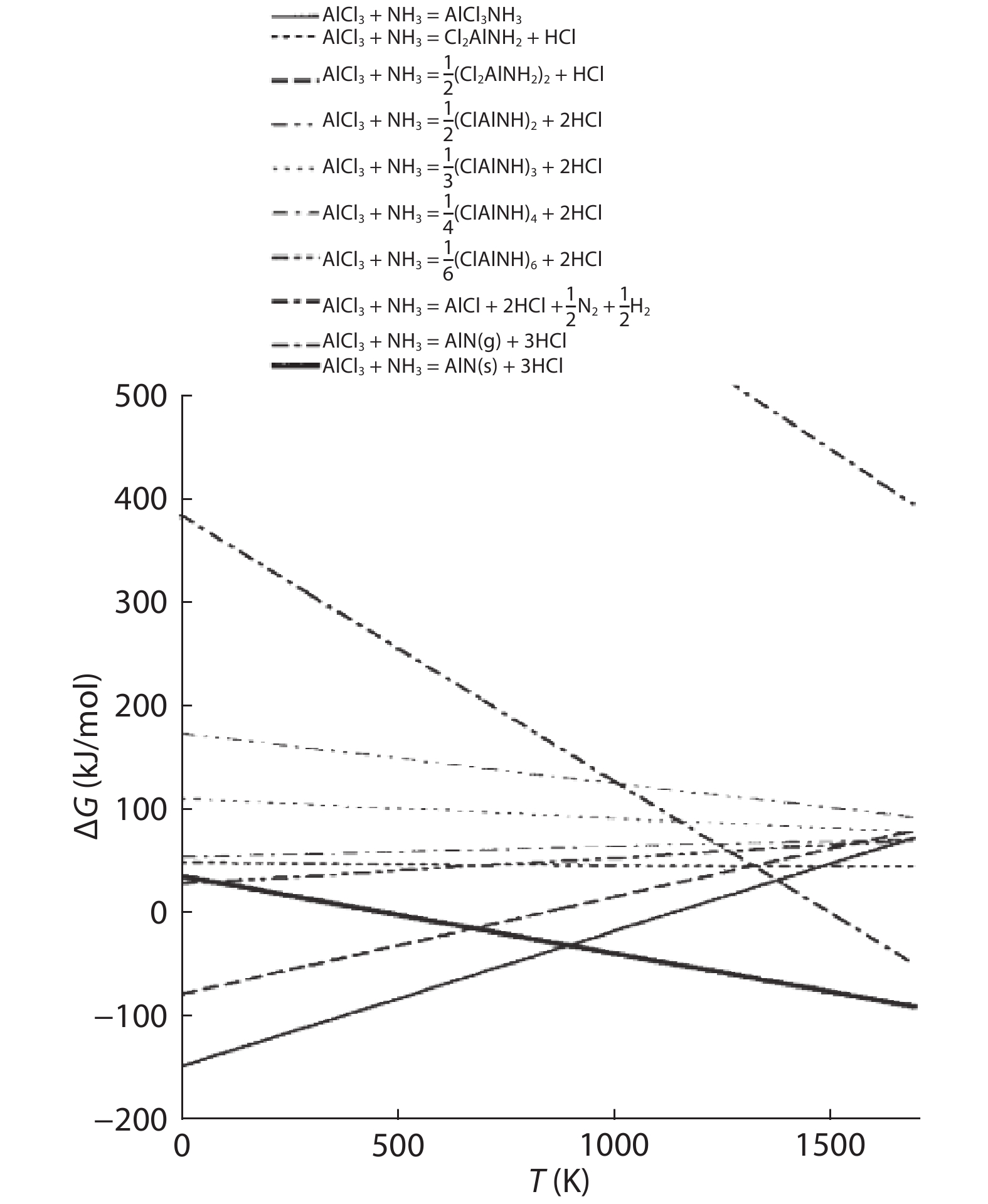
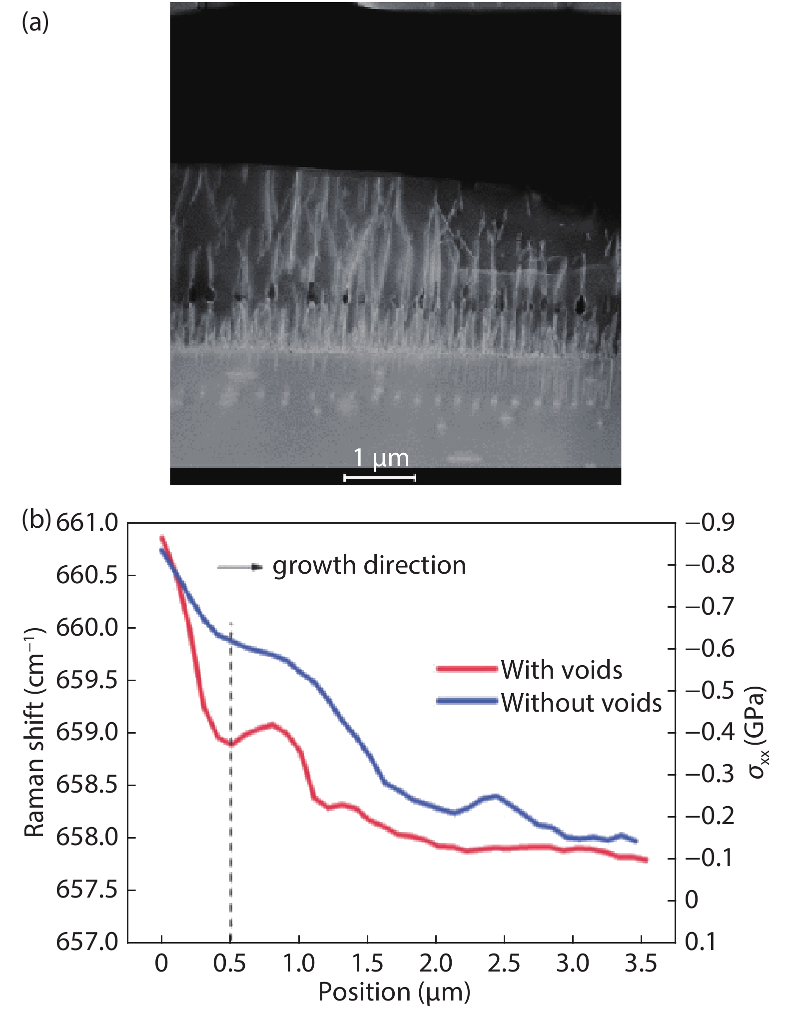
Fig. 1.
Gibbs energy diagram for different chemical species during the growth AlN grown by CVD[34].
REVIEWS
Maosong Sun1, 2, Jinfeng Li1, Jicai Zhang1, 2, and Wenhong Sun2, 3
Corresponding author: Jicai Zhang, Email: jczhang@mail.buct.edu.cn
Abstract: Aluminum nitride (AlN) is the promising substrates material for the epitaxial growth of III-nitrides devices, such as high-power, high-frequency electronic, deep ultraviolet optoelectronics and acoustic devices. However, it is rather difficult to obtain the high quality and crack-free thick AlN wafers because of the low surface migration of Al adatoms and the large thermal and lattice mismatches between the foreign substrates and AlN. In this work, the fabrication of AlN material by hydride vapor phase epitaxy (HVPE) was summarized and discussed. At last, the outlook of the production of AlN by HVPE was prospected.
Keywords: hydride vapor phase epitaxy, aluminum nitride, templates, free standing substrate
| [1] |
Avrutin V, Silversmith D J, Mori Y, et al. Growth of bulk GaN and AlN: progress and challenges. Proc IEEE, 2010, 98, 1302 doi: 10.1109/JPROC.2010.2044967
|
| [2] |
Paskova T, Hanser D A, Evans K R. GaN substrates for III-nitride devices. Proc IEEE, 2010, 98, 1324 doi: 10.1109/JPROC.2009.2030699
|
| [3] |
Mishra U K, Parikh P, Wu Y F. AlGaN/GaN HEMTs — An overview of device operation and applications. Proc IEEE, 2002, 90, 1022 doi: 10.1109/JPROC.2002.1021567
|
| [4] |
Adivarahan V, Sun W H, Chitnis A, et al. 250 nm AlGaN light-emitting diodes. Appl Phys Lett, 2004, 85, 2175 doi: 10.1063/1.1796525
|
| [5] |
Hirayama H, Yatabe T, Noguchi N, et al. 231–261 nm AlGaN deep-ultraviolet light-emitting diodes fabricated on AlN multilayer buffers grown by ammonia pulse-flow method on sapphire. Appl Phys Lett, 2007, 91, 071901 doi: 10.1063/1.2770662
|
| [6] |
Jain R, Sun W, Yang J, et al. Migration enhanced lateral epitaxial overgrowth of AlN and AlGaN for high reliability deep ultraviolet light emitting diodes. Appl Phys Lett, 2008, 93, 051113 doi: 10.1063/1.2969402
|
| [7] |
Zhang J C, Zhu Y H, Egawa T, et al. Suppression of the subband parasitic peak by 1 nm i-AlN interlayer in AlGaN deep ultraviolet light-emitting diodes. Appl Phys Lett, 2008, 93, 131117 doi: 10.1063/1.2996580
|
| [8] |
Hirayama H, Fujikawa S, Noguchi N, et al. 222–282 nm AlGaN and InAlGaN-based deep-UV LEDs fabricated on high-quality AlN on sapphire. Phys Status Solidi A, 2009, 206, 1176 doi: 10.1002/pssa.200880961
|
| [9] |
Susilo N, Hagedorn S, D, Jaeger D, et al. AlGaN-based deep UV LEDs grown on sputtered and high temperature annealed AlN/sapphire. Appl Phys Lett, 2018, 112, 041110 doi: 10.1063/1.5010265
|
| [10] |
Adivarahan V, Wu S, Sun W H, et al. High-power deep ultraviolet light-emitting diodes based on a micro-pixel design. Appl Phys Lett, 2004, 85, 1838 doi: 10.1063/1.1784882
|
| [11] |
Sun W H, Zhang J P, Adivarahan V, et al. AlGaN-based 280 nm light-emitting diodes with continuous wave powers in excess of 1.5 mW. Appl Phys Lett, 2004, 85, 531 doi: 10.1063/1.1772864
|
| [12] |
Zhang J C, Zhu Y H, Egawa T, et al. Quantum-well and localized state emissions in AlInGaN deep ultraviolet light-emitting diodes. Appl Phys Lett, 2007, 91, 221906 doi: 10.1063/1.2817947
|
| [13] |
Zhang J C, Sakai Y, Egawa T. Low-temperature electroluminescence quenching of AlGaN deep ultraviolet light-emitting diodes. Appl Phys Lett, 2010, 96, 013503 doi: 10.1063/1.3284521
|
| [14] |
Shatalov M, Sun W H, Lunev A, et al. AlGaN deep-ultraviolet light-emitting diodes with external quantum efficiency above 10%. Appl Phys Express, 2012, 5, 082101 doi: 10.1143/APEX.5.082101
|
| [15] |
Tan S X, Zhang J C, Egawa T, et al. Influence of quantum-well width on the electroluminescence properties of AlGaN deep ultraviolet light-emitting diodes at different temperatures. Nanoscale Res Lett, 2018, 13, 334 doi: 10.1186/s11671-018-2756-2
|
| [16] |
Kneissl M, Kolbe T, Chua C, et al. Advances in group III-nitride-based deep UV light-emitting diode technology. Semicond Sci Tech, 2011, 26, 014036 doi: 10.1088/0268-1242/26/1/014036
|
| [17] |
Yano M, Okamoto M, Yap Y K, et al. Growth of nitride crystals, BN, AlN and GaN by using a Na flux. Diam Relat Mater, 2000, 9, 512 doi: 10.1016/S0925-9635(99)00308-8
|
| [18] |
Kangawa Y, Toki R, Yayama T, et al. Novel solution growth method of bulk AlN using Al and Li3N solid sources. Appl Phys Express, 2011, 4, 095501 doi: 10.1143/APEX.4.095501
|
| [19] |
Wang B G, Callahan M J. Ammonothermal synthesis of III-nitride crystals. Cryst Growth Des, 2006, 6, 1227 doi: 10.1021/cg050271r
|
| [20] |
Slack G A, Mcnelly T F. Growth of high-purity AlN crystals. J Cryst Growth, 1976, 34, 263 doi: 10.1016/0022-0248(76)90139-1
|
| [21] |
Herro Z G, Zhuang D, Schlesser R, et al. Growth of AlN single crystalline boules. J Cryst Growth, 2010, 312, 2519 doi: 10.1016/j.jcrysgro.2010.04.005
|
| [22] |
Bondokov R T, Mueller S G, Morgan K E, et al. Large-area AlN substrates for electronic applications: An industrial perspective. J Cryst Growth, 2008, 310, 4020 doi: 10.1016/j.jcrysgro.2008.06.032
|
| [23] |
Makarov Y N, Avdeev O V, Barash I S, et al. Experimental and theoretical analysis of sublimation growth of AlN bulk crystals. J Cryst Growth, 2008, 310, 881 doi: 10.1016/j.jcrysgro.2007.11.059
|
| [24] |
Hartmann C, Dittmar A, Wollweber J, et al. Bulk AlN growth by physical vapour transport. Semicond Sci Tech, 2014, 29, 084002 doi: 10.1088/0268-1242/29/8/084002
|
| [25] |
Bai J, Dudley M, Sun W H, et al. Reduction of threading dislocation densities in AlN/sapphire epilayers driven by growth mode modification. Appl Phys Lett, 2006, 88, 051903 doi: 10.1063/1.2170407
|
| [26] |
Imura M, Fujimoto N, Okada N, et al. Annihilation mechanism of threading dislocations in AlN grown by growth form modification, method using V/III ratio. J Cryst Growth, 2007, 300, 136 doi: 10.1016/j.jcrysgro.2006.11.013
|
| [27] |
Banal R G, Funato M, Kawakamia Y. Initial nucleation of AlN grown directly on sapphire substrates by metal-organic vapor phase epitaxy. Appl Phys Lett, 2008, 92, 241905 doi: 10.1063/1.2937445
|
| [28] |
Takeuchi M, Ooishi S, Ohtsuka T, et al. Improvement of AI-polar AIN layer quality by three-stage flow-modulation metalorganic chemical vapor deposition. Appl Phys Express, 2008, 1, 021102 doi: 10.1143/APEX.1.021102
|
| [29] |
Zhang L S, Xu F J, Wang J M, et al. High-quality AlN epitaxy on nano-patterned sapphire substrates prepared by nano-imprint lithography. Sci Rep-Uk, 2016, 6, 35934 doi: 10.1038/srep35934
|
| [30] |
Lee D, Lee J W, Jang J, et al. Improved performance of AlGaN-based deep ultraviolet light-emitting diodes with nano-patterned AlN/sapphire substrates. Appl Phys Lett, 2017, 110, 191103 doi: 10.1063/1.4983283
|
| [31] |
Long H L, Dai J N, Zhang Y, et al. High quality 10.6 μm AIN grown on pyramidal patterned sapphire substrate by MOCVD. Appl Phys Lett, 2019, 114, 042101 doi: 10.1063/1.5074177
|
| [32] |
Freitas J A, Braga G C B, Moore W J, et al. Structural and optical properties of thick freestanding GaN templates. J Cryst Growth, 2001, 231, 322 doi: 10.1016/S0022-0248(01)01456-7
|
| [33] |
Liu L, Edgar J H. Substrates for gallium nitride epitaxy. Mat Sci Eng R, 2002, 37, 61 doi: 10.1016/S0927-796X(02)00008-6
|
| [34] |
Timoshkin A Y, Bettinger H F, Schaefer H F. The chemical vapor deposition of aluminum nitride: Unusual cluster formation in the gas phase. J Am Chem Soc, 1997, 119, 5668 doi: 10.1021/ja964163s
|
| [35] |
Kumagai Y, Yamane T, Miyaji T, et al. Hydride vapor phase epitaxy of AlN: thermodynamic analysis of aluminum source and its application to growth. Phys Status Solidi C, 2003, 0, 2498 doi: 10.1002/pssc.200303360
|
| [36] |
Ledyaev O Y, Cherenkov A E, Nikolaev A E, et al. Properties of AlN layers grown on SiC substrates in wide temperature range by HVPE. International Workshop on Nitride Semiconductors, Proceedings, 2002, 474
|
| [37] |
Nikolaev A, Nikitina I, Zubrilov A, et al. AlN wafers fabricated by hydride vapor phase epitaxy. MRS Internet J N S R, 2000, 5, W6.5
|
| [38] |
Melnik Y, Tsvetkov D, Pechnikov A, et al. Characterization of AlN/SiC epitaxial wafers fabricated by hydride vapour phase epitaxy. Phys Status Solidi A, 2001, 188, 463 doi: 10.1002/1521-396X(200111)188:1<463::AID-PSSA463>3.0.CO;2-H
|
| [39] |
Melnik Y, Soukhoveev V, Ivantsov V, et al. AlN substrates: fabrication via vapor phase growth and characterization. Phys Status Solidi A, 2003, 200, 22 doi: 10.1002/pssa.200303522
|
| [40] |
Kovalenkov O, Soukhoveev V, Ivantsov V, et al. Thick AlN layers grown by HVPE. J Cryst Growth, 2005, 281, 87 doi: 10.1016/j.jcrysgro.2005.03.054
|
| [41] |
Kumagai Y, Yamane T, Koukitu A. Growth of thick AlN layers by hydride vapor-phase epitaxy. J Cryst Growth, 2005, 281, 62 doi: 10.1016/j.jcrysgro.2005.03.011
|
| [42] |
Liu Y H, Tanabe T, Miyake H, et al. Fabrication of thick AlN film by low pressure hydride vapor phase epitaxy. Phys Status Solidi C, 2006, 3, 1479 doi: 10.1002/pssc.200565355
|
| [43] |
Liu Y H, Tanabe T, Miyake H, et al. Growth of thick AlN layer by hydride vapor phase epitaxy. Jpn J Appl Phys Part 2, 2005, 44, 505 doi: 10.1143/JJAP.44.L505
|
| [44] |
Sun M S, Zhang J C, Huang J, et al. AlN thin film grown on different substrates by hydride vapor phase epitaxy. J Cryst Growth, 2016, 436, 62 doi: 10.1016/j.jcrysgro.2015.11.040
|
| [45] |
Gong X J, Xu K, Huang J, et al. Evolution of the surface morphology of AlN epitaxial film by HVPE. J Cryst Growth, 2015, 409, 100 doi: 10.1016/j.jcrysgro.2014.10.012
|
| [46] |
Eriguchi K I, Murakami H, Panyukova U, et al. MOVPE-like HVPE of AlN using solid aluminum trichloride source. J Cryst Growth, 2007, 298, 332 doi: 10.1016/j.jcrysgro.2006.10.035
|
| [47] |
Coudurier N, Boichot R, Fellmann V, et al. Effects of the V/III ratio on the quality of aluminum nitride grown on (0001) sapphire by high temperature hydride vapor phase epitaxy. Phys Status Solidi C, 2013, 10, 362 doi: 10.1002/pssc.201200686
|
| [48] |
Claudel A, Fellmanna V, Gelard I, et al. Influence of the V/III ratio in the gas phase on thin epitaxial AlN layers grown on (0001) sapphire by high temperature hydride vapor phase epitaxy. Thin Solid Films, 2014, 573, 140 doi: 10.1016/j.tsf.2014.11.022
|
| [49] |
Nagashima T, Harada M, Yanagi H, et al. High-speed epitaxial growth of AlN above 1200 °C by hydride vapor phase epitaxy. J Cryst Growth, 2007, 300, 42 doi: 10.1016/j.jcrysgro.2006.10.260
|
| [50] |
Amano H, Sawaki N, Akasaki I, et al. Metalorganic vapor-phase epitaxial-growth of a high-quality gan film using an AlN buffer layer. Appl Phys Lett, 1986, 48, 353 doi: 10.1063/1.96549
|
| [51] |
Usui A, Sunakawa H, Sakai A, et al. Thick GaN epitaxial growth with low dislocation density by hydride vapor phase epitaxy. Jpn J Appl Phys Part 2, 1997, 36, L899 doi: 10.1143/JJAP.36.L899
|
| [52] |
Ambacher O. Growth and applications of Group III nitrides. J Phys D, 1998, 31, 2653 doi: 10.1088/0022-3727/31/20/001
|
| [53] |
Wu X H, Kapolnek D, Tarsa E J, et al. Nucleation layer evolution in metal-organic chemical vapor deposition grown GaN. Appl Phys Lett, 1996, 68, 1371 doi: 10.1063/1.116083
|
| [54] |
Nagashima T, Ma M H, Yanagi H, et al. Improvement of AlN crystalline quality with high epitaxial growth rates by hydride vapor phase epitaxy. J Cryst Growth, 2007, 305, 355 doi: 10.1016/j.jcrysgro.2007.04.001
|
| [55] |
Su X J, Zhang J C, Huang J, et al. Defect structure of high temperature hydride vapor phase epitaxy-grown epitaxial (0001) AlN/sapphire using growth mode modification process. J Cryst Growth, 2017, 467, 82 doi: 10.1016/j.jcrysgro.2017.03.031
|
| [56] |
Akiyama K, Araki T, Murakami H, et al. In situ gravimetric monitoring of decomposition rate on the surface of (0001) c-plane sapphire for the high temperature growth of AlN. Phys Status Solidi C, 2007, 4, 2297 doi: 10.1002/pssc.200674816
|
| [57] |
Zhao D G, Zhu J J, Liu Z S, et al. Surface morphology of AlN buffer layer and its effect on GaN growth by metalorganic chemical vapor deposition. Appl Phys Lett, 2004, 85, 1499 doi: 10.1063/1.1784034
|
| [58] |
Tsujisawa K, Kishino S, Liu Y H, et al. High temperature growth of AlN film by LP-HVPE. Phys Status Solidi C, 2007, 4, 2252 doi: 10.1002/pssc.200674814
|
| [59] |
Tajima J, Murakami H, Kumagai Y, et al. Preparation of a crack-free AlN template layer on sapphire substrate by hydride vapor-phase epitaxy at 1450 °C. J Cryst Growth, 2009, 311, 2837 doi: 10.1016/j.jcrysgro.2009.01.024
|
| [60] |
Tajima J, Kubota Y, Togashi R, et al. Growth of thin protective AlN layers on sapphire substrates at 1065 °C for hydride vapor phase epitaxy of AlN above 1300 °C. Phys Status Solidi C, 2008, 5, 1515 doi: 10.1002/pssc.200778433
|
| [61] |
Balaji M, Claudel A, Fellmann V, et al. Effects of AlN nucleation layers on the growth of AlN films using high temperature hydride vapor phase epitaxy. J Alloy Compd, 2012, 526, 103 doi: 10.1016/j.jallcom.2012.02.111
|
| [62] |
Miyake H, Nishio G, Suzuki S, et al. Annealing of an AlN buffer layer in N2–CO for growth of a high-quality AlN film on sapphire. Appl Phys Express, 2016, 9, 025501 doi: 10.7567/APEX.9.025501
|
| [63] |
Huang J, Niu M T, Zhang J C, et al. Reduction of threading dislocation density for AlN epilayer via a highly compressive-stressed buffer layer. J Cryst Growth, 2017, 459, 159 doi: 10.1016/j.jcrysgro.2016.11.086
|
| [64] |
Su X J, Huang J, Zhang J P, et al. Microstructure and influence of buffer layer on threading dislocations in (0001) AlN/sapphire grown by hydride vapor phase epitaxy. J Cryst Growth, 2019, 515, 72 doi: 10.1016/j.jcrysgro.2019.03.012
|
| [65] |
Imura M, Nakano K, Narita G, et al. Epitaxial lateral overgrowth of AlN on trench-patterned AlN layers. J Cryst Growth, 2007, 298, 257 doi: 10.1016/j.jcrysgro.2006.10.043
|
| [66] |
Katagiri Y, Kishino S, Okuura K, et al. Low-pressure HVPE growth of crack-free thick AlN on a trench-patterned AlN template. J Cryst Growth, 2009, 311, 2831 doi: 10.1016/j.jcrysgro.2009.01.022
|
| [67] |
Okumura K, Nomura T, Miyake H, et al. HVPE growth of AlN on trench-patterned 6H-SiC substrates. Phys Status Solidi C, 2011, 8, 467 doi: 10.1002/pssc.201000584
|
| [68] |
Lee G S, Lee C, Jeon H, et al. Growth of AlN layer on patterned sapphire substrate by hydride vapor phase epitaxy. Jpn J Appl Phys, 2016, 55, 05FC02 doi: 10.7567/JJAP.55.05FC02
|
| [69] |
Xiao S Y, Suzuki R, Miyake H, et al. Improvement mechanism of sputtered AlN films by high-temperature annealing. J Cryst Growth, 2018, 502, 41 doi: 10.1016/j.jcrysgro.2018.09.002
|
| [70] |
Xiao S, Jiang N, Shojiki K, et al. Preparation of high-quality thick AlN layer on nanopatterned sapphire substrates with sputter-deposited annealed AlN film by hydride vapor-phase epitaxy. Jpn J Appl Phys, 2019, 58, SC1003 doi: 10.7567/1347-4065/ab0ad4
|
| [71] |
Liu X H, Zhang J C, Su X J, et al. Fabrication of crack-free AlN film on sapphire by hydride vapor phase epitaxy using an in situ etching method. Appl Phys Express, 2016, 9 doi: 10.7567/APEX.9.045501
|
| [72] |
Prokofyeva T, Seon M, Vanbuskirk J, et al. Vibrational properties of AlN grown on (111)-oriented silicon. Phys Rev B, 2001, 63, 125313 doi: 10.1103/PhysRevB.63.125313
|
| [73] |
Huang Z P, Geyer N, Werner P, et al. Metal-assisted chemical etching of silicon: a review. Adv Mater, 2011, 23, 285 doi: 10.1002/adma.201001784
|
| [74] |
Akiyama K, Murakami H, Kumaga Y, et al. In situ gravimetric monitoring of decomposition rate on surface of (10(1)over-bar2) r-plane sapphire for high-temperature growth of nonpolar AlN. Jpn J Appl Phys, 2008, 47, 3434 doi: 10.1143/JJAP.47.3434
|
| [75] |
Kumagai Y, Akiyama K, Togashi R, et al. Polarity dependence of AlN {0001} decomposition in flowing H2. J Cryst Growth, 2007, 305, 366 doi: 10.1016/j.jcrysgro.2007.04.005
|
| [76] |
Kumagai Y, Enatsu Y, Ishizuki M, et al. Investigation of void formation beneath thin AlN layers by decomposition of sapphire substrates for self-separation of thick AlN layers grown by HVPE. J Cryst Growth, 2010, 312, 2530 doi: 10.1016/j.jcrysgro.2010.04.008
|
| [77] |
Kumagai Y, Tajima J, Ishizuki M, et al. Self-separation of a thick AIN layer from a sapphire substrate via interfacial voids formed by the decomposition of sapphire. Appl Phys Express, 2008, 1, 045003 doi: 10.1143/APEX.1.045003
|
| [78] |
Sun M S, Zhang J C, Huang J, et al. Influence of thickness on strain state and surface morphology of AlN grown by HVPE. J Semicond, 2016, 37, 045501 doi: CNKI:SUN:BDTX.0.2016-12-004
|
| [79] |
Kumagai Y, Kubota Y, Nagashima T, et al. Preparation of a freestanding AIN substrate from a thick AIN layer grown by hydride vapor phase epitaxy on a bulk AIN substrate prepared by physical vapor transport. Appl Phys Express, 2012, 5, 055504 doi: 10.1143/APEX.5.055504
|
| [80] |
Nomura T, Okumura K, Miyake H, et al. AIN homoepitaxial growth on sublimation-AIN substrate by low-pressure HVPE. J Cryst Growth, 2012, 350, 69 doi: 10.1016/j.jcrysgro.2011.12.025
|
| [81] |
Nagashima T, Hakomori A, Shimoda T, et al. Preparation of freestanding AlN substrates by hydride vapor phase epitaxy using hybrid seed substrates. J Cryst Growth, 2012, 350, 75 doi: 10.1016/j.jcrysgro.2011.12.027
|
| [82] |
Watanabe Y, Miyake H, Hiramatsu K, et al. HVPE homoepitaxy on freestanding AlN substrate with trench pattern. Phys Status Solidi C, 2015, 12, 334 doi: 10.1002/pssc.201400202
|
| [83] |
Kumagai Y, Nagashima T, Koukitu A. Preparation of a freestanding AlN substrate by hydride vapor phase epitaxy at 1230 °C using (111) Si as a starting substrate. Jpn J Appl Phys Part 2, 2007, 46, L389 doi: 10.1143/JJAP.46.L389
|
| [84] |
Freitas J A, Culbertson J C, Mastro M A, et al. Structural and optical properties of thick freestanding AlN films prepared by hydride vapor phase epitaxy. J Cryst Growth, 2012, 350, 33 doi: 10.1016/j.jcrysgro.2011.12.018
|
| [85] |
Soukhoveev V, Volkova A, Ivantsov V, et al. Large area GaN and AlN template substrates fabricated by HVPE. Phys Status Solidi C, 2009, 6, S333 doi: 10.1002/pssc.200880906
|


Article views: 6406 Times PDF downloads: 259 Times Cited by: 0 Times
Received: 25 October 2019 Revised: 24 November 2019 Online: Accepted Manuscript: 26 November 2019Uncorrected proof: 27 November 2019Published: 09 December 2019
| Citation: |
Maosong Sun, Jinfeng Li, Jicai Zhang, Wenhong Sun. The fabrication of AlN by hydride vapor phase epitaxy[J]. Journal of Semiconductors, 2019, 40(12): 121803. doi: 10.1088/1674-4926/40/12/121803
****
M S Sun, J F Li, J C Zhang, W H Sun, The fabrication of AlN by hydride vapor phase epitaxy[J]. J. Semicond., 2019, 40(12): 121803. doi: 10.1088/1674-4926/40/12/121803.

|
| [1] |
Avrutin V, Silversmith D J, Mori Y, et al. Growth of bulk GaN and AlN: progress and challenges. Proc IEEE, 2010, 98, 1302 doi: 10.1109/JPROC.2010.2044967
|
| [2] |
Paskova T, Hanser D A, Evans K R. GaN substrates for III-nitride devices. Proc IEEE, 2010, 98, 1324 doi: 10.1109/JPROC.2009.2030699
|
| [3] |
Mishra U K, Parikh P, Wu Y F. AlGaN/GaN HEMTs — An overview of device operation and applications. Proc IEEE, 2002, 90, 1022 doi: 10.1109/JPROC.2002.1021567
|
| [4] |
Adivarahan V, Sun W H, Chitnis A, et al. 250 nm AlGaN light-emitting diodes. Appl Phys Lett, 2004, 85, 2175 doi: 10.1063/1.1796525
|
| [5] |
Hirayama H, Yatabe T, Noguchi N, et al. 231–261 nm AlGaN deep-ultraviolet light-emitting diodes fabricated on AlN multilayer buffers grown by ammonia pulse-flow method on sapphire. Appl Phys Lett, 2007, 91, 071901 doi: 10.1063/1.2770662
|
| [6] |
Jain R, Sun W, Yang J, et al. Migration enhanced lateral epitaxial overgrowth of AlN and AlGaN for high reliability deep ultraviolet light emitting diodes. Appl Phys Lett, 2008, 93, 051113 doi: 10.1063/1.2969402
|
| [7] |
Zhang J C, Zhu Y H, Egawa T, et al. Suppression of the subband parasitic peak by 1 nm i-AlN interlayer in AlGaN deep ultraviolet light-emitting diodes. Appl Phys Lett, 2008, 93, 131117 doi: 10.1063/1.2996580
|
| [8] |
Hirayama H, Fujikawa S, Noguchi N, et al. 222–282 nm AlGaN and InAlGaN-based deep-UV LEDs fabricated on high-quality AlN on sapphire. Phys Status Solidi A, 2009, 206, 1176 doi: 10.1002/pssa.200880961
|
| [9] |
Susilo N, Hagedorn S, D, Jaeger D, et al. AlGaN-based deep UV LEDs grown on sputtered and high temperature annealed AlN/sapphire. Appl Phys Lett, 2018, 112, 041110 doi: 10.1063/1.5010265
|
| [10] |
Adivarahan V, Wu S, Sun W H, et al. High-power deep ultraviolet light-emitting diodes based on a micro-pixel design. Appl Phys Lett, 2004, 85, 1838 doi: 10.1063/1.1784882
|
| [11] |
Sun W H, Zhang J P, Adivarahan V, et al. AlGaN-based 280 nm light-emitting diodes with continuous wave powers in excess of 1.5 mW. Appl Phys Lett, 2004, 85, 531 doi: 10.1063/1.1772864
|
| [12] |
Zhang J C, Zhu Y H, Egawa T, et al. Quantum-well and localized state emissions in AlInGaN deep ultraviolet light-emitting diodes. Appl Phys Lett, 2007, 91, 221906 doi: 10.1063/1.2817947
|
| [13] |
Zhang J C, Sakai Y, Egawa T. Low-temperature electroluminescence quenching of AlGaN deep ultraviolet light-emitting diodes. Appl Phys Lett, 2010, 96, 013503 doi: 10.1063/1.3284521
|
| [14] |
Shatalov M, Sun W H, Lunev A, et al. AlGaN deep-ultraviolet light-emitting diodes with external quantum efficiency above 10%. Appl Phys Express, 2012, 5, 082101 doi: 10.1143/APEX.5.082101
|
| [15] |
Tan S X, Zhang J C, Egawa T, et al. Influence of quantum-well width on the electroluminescence properties of AlGaN deep ultraviolet light-emitting diodes at different temperatures. Nanoscale Res Lett, 2018, 13, 334 doi: 10.1186/s11671-018-2756-2
|
| [16] |
Kneissl M, Kolbe T, Chua C, et al. Advances in group III-nitride-based deep UV light-emitting diode technology. Semicond Sci Tech, 2011, 26, 014036 doi: 10.1088/0268-1242/26/1/014036
|
| [17] |
Yano M, Okamoto M, Yap Y K, et al. Growth of nitride crystals, BN, AlN and GaN by using a Na flux. Diam Relat Mater, 2000, 9, 512 doi: 10.1016/S0925-9635(99)00308-8
|
| [18] |
Kangawa Y, Toki R, Yayama T, et al. Novel solution growth method of bulk AlN using Al and Li3N solid sources. Appl Phys Express, 2011, 4, 095501 doi: 10.1143/APEX.4.095501
|
| [19] |
Wang B G, Callahan M J. Ammonothermal synthesis of III-nitride crystals. Cryst Growth Des, 2006, 6, 1227 doi: 10.1021/cg050271r
|
| [20] |
Slack G A, Mcnelly T F. Growth of high-purity AlN crystals. J Cryst Growth, 1976, 34, 263 doi: 10.1016/0022-0248(76)90139-1
|
| [21] |
Herro Z G, Zhuang D, Schlesser R, et al. Growth of AlN single crystalline boules. J Cryst Growth, 2010, 312, 2519 doi: 10.1016/j.jcrysgro.2010.04.005
|
| [22] |
Bondokov R T, Mueller S G, Morgan K E, et al. Large-area AlN substrates for electronic applications: An industrial perspective. J Cryst Growth, 2008, 310, 4020 doi: 10.1016/j.jcrysgro.2008.06.032
|
| [23] |
Makarov Y N, Avdeev O V, Barash I S, et al. Experimental and theoretical analysis of sublimation growth of AlN bulk crystals. J Cryst Growth, 2008, 310, 881 doi: 10.1016/j.jcrysgro.2007.11.059
|
| [24] |
Hartmann C, Dittmar A, Wollweber J, et al. Bulk AlN growth by physical vapour transport. Semicond Sci Tech, 2014, 29, 084002 doi: 10.1088/0268-1242/29/8/084002
|
| [25] |
Bai J, Dudley M, Sun W H, et al. Reduction of threading dislocation densities in AlN/sapphire epilayers driven by growth mode modification. Appl Phys Lett, 2006, 88, 051903 doi: 10.1063/1.2170407
|
| [26] |
Imura M, Fujimoto N, Okada N, et al. Annihilation mechanism of threading dislocations in AlN grown by growth form modification, method using V/III ratio. J Cryst Growth, 2007, 300, 136 doi: 10.1016/j.jcrysgro.2006.11.013
|
| [27] |
Banal R G, Funato M, Kawakamia Y. Initial nucleation of AlN grown directly on sapphire substrates by metal-organic vapor phase epitaxy. Appl Phys Lett, 2008, 92, 241905 doi: 10.1063/1.2937445
|
| [28] |
Takeuchi M, Ooishi S, Ohtsuka T, et al. Improvement of AI-polar AIN layer quality by three-stage flow-modulation metalorganic chemical vapor deposition. Appl Phys Express, 2008, 1, 021102 doi: 10.1143/APEX.1.021102
|
| [29] |
Zhang L S, Xu F J, Wang J M, et al. High-quality AlN epitaxy on nano-patterned sapphire substrates prepared by nano-imprint lithography. Sci Rep-Uk, 2016, 6, 35934 doi: 10.1038/srep35934
|
| [30] |
Lee D, Lee J W, Jang J, et al. Improved performance of AlGaN-based deep ultraviolet light-emitting diodes with nano-patterned AlN/sapphire substrates. Appl Phys Lett, 2017, 110, 191103 doi: 10.1063/1.4983283
|
| [31] |
Long H L, Dai J N, Zhang Y, et al. High quality 10.6 μm AIN grown on pyramidal patterned sapphire substrate by MOCVD. Appl Phys Lett, 2019, 114, 042101 doi: 10.1063/1.5074177
|
| [32] |
Freitas J A, Braga G C B, Moore W J, et al. Structural and optical properties of thick freestanding GaN templates. J Cryst Growth, 2001, 231, 322 doi: 10.1016/S0022-0248(01)01456-7
|
| [33] |
Liu L, Edgar J H. Substrates for gallium nitride epitaxy. Mat Sci Eng R, 2002, 37, 61 doi: 10.1016/S0927-796X(02)00008-6
|
| [34] |
Timoshkin A Y, Bettinger H F, Schaefer H F. The chemical vapor deposition of aluminum nitride: Unusual cluster formation in the gas phase. J Am Chem Soc, 1997, 119, 5668 doi: 10.1021/ja964163s
|
| [35] |
Kumagai Y, Yamane T, Miyaji T, et al. Hydride vapor phase epitaxy of AlN: thermodynamic analysis of aluminum source and its application to growth. Phys Status Solidi C, 2003, 0, 2498 doi: 10.1002/pssc.200303360
|
| [36] |
Ledyaev O Y, Cherenkov A E, Nikolaev A E, et al. Properties of AlN layers grown on SiC substrates in wide temperature range by HVPE. International Workshop on Nitride Semiconductors, Proceedings, 2002, 474
|
| [37] |
Nikolaev A, Nikitina I, Zubrilov A, et al. AlN wafers fabricated by hydride vapor phase epitaxy. MRS Internet J N S R, 2000, 5, W6.5
|
| [38] |
Melnik Y, Tsvetkov D, Pechnikov A, et al. Characterization of AlN/SiC epitaxial wafers fabricated by hydride vapour phase epitaxy. Phys Status Solidi A, 2001, 188, 463 doi: 10.1002/1521-396X(200111)188:1<463::AID-PSSA463>3.0.CO;2-H
|
| [39] |
Melnik Y, Soukhoveev V, Ivantsov V, et al. AlN substrates: fabrication via vapor phase growth and characterization. Phys Status Solidi A, 2003, 200, 22 doi: 10.1002/pssa.200303522
|
| [40] |
Kovalenkov O, Soukhoveev V, Ivantsov V, et al. Thick AlN layers grown by HVPE. J Cryst Growth, 2005, 281, 87 doi: 10.1016/j.jcrysgro.2005.03.054
|
| [41] |
Kumagai Y, Yamane T, Koukitu A. Growth of thick AlN layers by hydride vapor-phase epitaxy. J Cryst Growth, 2005, 281, 62 doi: 10.1016/j.jcrysgro.2005.03.011
|
| [42] |
Liu Y H, Tanabe T, Miyake H, et al. Fabrication of thick AlN film by low pressure hydride vapor phase epitaxy. Phys Status Solidi C, 2006, 3, 1479 doi: 10.1002/pssc.200565355
|
| [43] |
Liu Y H, Tanabe T, Miyake H, et al. Growth of thick AlN layer by hydride vapor phase epitaxy. Jpn J Appl Phys Part 2, 2005, 44, 505 doi: 10.1143/JJAP.44.L505
|
| [44] |
Sun M S, Zhang J C, Huang J, et al. AlN thin film grown on different substrates by hydride vapor phase epitaxy. J Cryst Growth, 2016, 436, 62 doi: 10.1016/j.jcrysgro.2015.11.040
|
| [45] |
Gong X J, Xu K, Huang J, et al. Evolution of the surface morphology of AlN epitaxial film by HVPE. J Cryst Growth, 2015, 409, 100 doi: 10.1016/j.jcrysgro.2014.10.012
|
| [46] |
Eriguchi K I, Murakami H, Panyukova U, et al. MOVPE-like HVPE of AlN using solid aluminum trichloride source. J Cryst Growth, 2007, 298, 332 doi: 10.1016/j.jcrysgro.2006.10.035
|
| [47] |
Coudurier N, Boichot R, Fellmann V, et al. Effects of the V/III ratio on the quality of aluminum nitride grown on (0001) sapphire by high temperature hydride vapor phase epitaxy. Phys Status Solidi C, 2013, 10, 362 doi: 10.1002/pssc.201200686
|
| [48] |
Claudel A, Fellmanna V, Gelard I, et al. Influence of the V/III ratio in the gas phase on thin epitaxial AlN layers grown on (0001) sapphire by high temperature hydride vapor phase epitaxy. Thin Solid Films, 2014, 573, 140 doi: 10.1016/j.tsf.2014.11.022
|
| [49] |
Nagashima T, Harada M, Yanagi H, et al. High-speed epitaxial growth of AlN above 1200 °C by hydride vapor phase epitaxy. J Cryst Growth, 2007, 300, 42 doi: 10.1016/j.jcrysgro.2006.10.260
|
| [50] |
Amano H, Sawaki N, Akasaki I, et al. Metalorganic vapor-phase epitaxial-growth of a high-quality gan film using an AlN buffer layer. Appl Phys Lett, 1986, 48, 353 doi: 10.1063/1.96549
|
| [51] |
Usui A, Sunakawa H, Sakai A, et al. Thick GaN epitaxial growth with low dislocation density by hydride vapor phase epitaxy. Jpn J Appl Phys Part 2, 1997, 36, L899 doi: 10.1143/JJAP.36.L899
|
| [52] |
Ambacher O. Growth and applications of Group III nitrides. J Phys D, 1998, 31, 2653 doi: 10.1088/0022-3727/31/20/001
|
| [53] |
Wu X H, Kapolnek D, Tarsa E J, et al. Nucleation layer evolution in metal-organic chemical vapor deposition grown GaN. Appl Phys Lett, 1996, 68, 1371 doi: 10.1063/1.116083
|
| [54] |
Nagashima T, Ma M H, Yanagi H, et al. Improvement of AlN crystalline quality with high epitaxial growth rates by hydride vapor phase epitaxy. J Cryst Growth, 2007, 305, 355 doi: 10.1016/j.jcrysgro.2007.04.001
|
| [55] |
Su X J, Zhang J C, Huang J, et al. Defect structure of high temperature hydride vapor phase epitaxy-grown epitaxial (0001) AlN/sapphire using growth mode modification process. J Cryst Growth, 2017, 467, 82 doi: 10.1016/j.jcrysgro.2017.03.031
|
| [56] |
Akiyama K, Araki T, Murakami H, et al. In situ gravimetric monitoring of decomposition rate on the surface of (0001) c-plane sapphire for the high temperature growth of AlN. Phys Status Solidi C, 2007, 4, 2297 doi: 10.1002/pssc.200674816
|
| [57] |
Zhao D G, Zhu J J, Liu Z S, et al. Surface morphology of AlN buffer layer and its effect on GaN growth by metalorganic chemical vapor deposition. Appl Phys Lett, 2004, 85, 1499 doi: 10.1063/1.1784034
|
| [58] |
Tsujisawa K, Kishino S, Liu Y H, et al. High temperature growth of AlN film by LP-HVPE. Phys Status Solidi C, 2007, 4, 2252 doi: 10.1002/pssc.200674814
|
| [59] |
Tajima J, Murakami H, Kumagai Y, et al. Preparation of a crack-free AlN template layer on sapphire substrate by hydride vapor-phase epitaxy at 1450 °C. J Cryst Growth, 2009, 311, 2837 doi: 10.1016/j.jcrysgro.2009.01.024
|
| [60] |
Tajima J, Kubota Y, Togashi R, et al. Growth of thin protective AlN layers on sapphire substrates at 1065 °C for hydride vapor phase epitaxy of AlN above 1300 °C. Phys Status Solidi C, 2008, 5, 1515 doi: 10.1002/pssc.200778433
|
| [61] |
Balaji M, Claudel A, Fellmann V, et al. Effects of AlN nucleation layers on the growth of AlN films using high temperature hydride vapor phase epitaxy. J Alloy Compd, 2012, 526, 103 doi: 10.1016/j.jallcom.2012.02.111
|
| [62] |
Miyake H, Nishio G, Suzuki S, et al. Annealing of an AlN buffer layer in N2–CO for growth of a high-quality AlN film on sapphire. Appl Phys Express, 2016, 9, 025501 doi: 10.7567/APEX.9.025501
|
| [63] |
Huang J, Niu M T, Zhang J C, et al. Reduction of threading dislocation density for AlN epilayer via a highly compressive-stressed buffer layer. J Cryst Growth, 2017, 459, 159 doi: 10.1016/j.jcrysgro.2016.11.086
|
| [64] |
Su X J, Huang J, Zhang J P, et al. Microstructure and influence of buffer layer on threading dislocations in (0001) AlN/sapphire grown by hydride vapor phase epitaxy. J Cryst Growth, 2019, 515, 72 doi: 10.1016/j.jcrysgro.2019.03.012
|
| [65] |
Imura M, Nakano K, Narita G, et al. Epitaxial lateral overgrowth of AlN on trench-patterned AlN layers. J Cryst Growth, 2007, 298, 257 doi: 10.1016/j.jcrysgro.2006.10.043
|
| [66] |
Katagiri Y, Kishino S, Okuura K, et al. Low-pressure HVPE growth of crack-free thick AlN on a trench-patterned AlN template. J Cryst Growth, 2009, 311, 2831 doi: 10.1016/j.jcrysgro.2009.01.022
|
| [67] |
Okumura K, Nomura T, Miyake H, et al. HVPE growth of AlN on trench-patterned 6H-SiC substrates. Phys Status Solidi C, 2011, 8, 467 doi: 10.1002/pssc.201000584
|
| [68] |
Lee G S, Lee C, Jeon H, et al. Growth of AlN layer on patterned sapphire substrate by hydride vapor phase epitaxy. Jpn J Appl Phys, 2016, 55, 05FC02 doi: 10.7567/JJAP.55.05FC02
|
| [69] |
Xiao S Y, Suzuki R, Miyake H, et al. Improvement mechanism of sputtered AlN films by high-temperature annealing. J Cryst Growth, 2018, 502, 41 doi: 10.1016/j.jcrysgro.2018.09.002
|
| [70] |
Xiao S, Jiang N, Shojiki K, et al. Preparation of high-quality thick AlN layer on nanopatterned sapphire substrates with sputter-deposited annealed AlN film by hydride vapor-phase epitaxy. Jpn J Appl Phys, 2019, 58, SC1003 doi: 10.7567/1347-4065/ab0ad4
|
| [71] |
Liu X H, Zhang J C, Su X J, et al. Fabrication of crack-free AlN film on sapphire by hydride vapor phase epitaxy using an in situ etching method. Appl Phys Express, 2016, 9 doi: 10.7567/APEX.9.045501
|
| [72] |
Prokofyeva T, Seon M, Vanbuskirk J, et al. Vibrational properties of AlN grown on (111)-oriented silicon. Phys Rev B, 2001, 63, 125313 doi: 10.1103/PhysRevB.63.125313
|
| [73] |
Huang Z P, Geyer N, Werner P, et al. Metal-assisted chemical etching of silicon: a review. Adv Mater, 2011, 23, 285 doi: 10.1002/adma.201001784
|
| [74] |
Akiyama K, Murakami H, Kumaga Y, et al. In situ gravimetric monitoring of decomposition rate on surface of (10(1)over-bar2) r-plane sapphire for high-temperature growth of nonpolar AlN. Jpn J Appl Phys, 2008, 47, 3434 doi: 10.1143/JJAP.47.3434
|
| [75] |
Kumagai Y, Akiyama K, Togashi R, et al. Polarity dependence of AlN {0001} decomposition in flowing H2. J Cryst Growth, 2007, 305, 366 doi: 10.1016/j.jcrysgro.2007.04.005
|
| [76] |
Kumagai Y, Enatsu Y, Ishizuki M, et al. Investigation of void formation beneath thin AlN layers by decomposition of sapphire substrates for self-separation of thick AlN layers grown by HVPE. J Cryst Growth, 2010, 312, 2530 doi: 10.1016/j.jcrysgro.2010.04.008
|
| [77] |
Kumagai Y, Tajima J, Ishizuki M, et al. Self-separation of a thick AIN layer from a sapphire substrate via interfacial voids formed by the decomposition of sapphire. Appl Phys Express, 2008, 1, 045003 doi: 10.1143/APEX.1.045003
|
| [78] |
Sun M S, Zhang J C, Huang J, et al. Influence of thickness on strain state and surface morphology of AlN grown by HVPE. J Semicond, 2016, 37, 045501 doi: CNKI:SUN:BDTX.0.2016-12-004
|
| [79] |
Kumagai Y, Kubota Y, Nagashima T, et al. Preparation of a freestanding AIN substrate from a thick AIN layer grown by hydride vapor phase epitaxy on a bulk AIN substrate prepared by physical vapor transport. Appl Phys Express, 2012, 5, 055504 doi: 10.1143/APEX.5.055504
|
| [80] |
Nomura T, Okumura K, Miyake H, et al. AIN homoepitaxial growth on sublimation-AIN substrate by low-pressure HVPE. J Cryst Growth, 2012, 350, 69 doi: 10.1016/j.jcrysgro.2011.12.025
|
| [81] |
Nagashima T, Hakomori A, Shimoda T, et al. Preparation of freestanding AlN substrates by hydride vapor phase epitaxy using hybrid seed substrates. J Cryst Growth, 2012, 350, 75 doi: 10.1016/j.jcrysgro.2011.12.027
|
| [82] |
Watanabe Y, Miyake H, Hiramatsu K, et al. HVPE homoepitaxy on freestanding AlN substrate with trench pattern. Phys Status Solidi C, 2015, 12, 334 doi: 10.1002/pssc.201400202
|
| [83] |
Kumagai Y, Nagashima T, Koukitu A. Preparation of a freestanding AlN substrate by hydride vapor phase epitaxy at 1230 °C using (111) Si as a starting substrate. Jpn J Appl Phys Part 2, 2007, 46, L389 doi: 10.1143/JJAP.46.L389
|
| [84] |
Freitas J A, Culbertson J C, Mastro M A, et al. Structural and optical properties of thick freestanding AlN films prepared by hydride vapor phase epitaxy. J Cryst Growth, 2012, 350, 33 doi: 10.1016/j.jcrysgro.2011.12.018
|
| [85] |
Soukhoveev V, Volkova A, Ivantsov V, et al. Large area GaN and AlN template substrates fabricated by HVPE. Phys Status Solidi C, 2009, 6, S333 doi: 10.1002/pssc.200880906
|

 WeChat ID
Journal of Semiconductors © 2017 All Rights Reserved 京ICP备05085259号-2

 DownLoad: