J. Semicond. > 2019, Volume 40 > Issue 3 > 032801

ARTICLES

Bandgap engineered novel g-C3N4/G/h-BN heterostructure for electronic applications

Santosh Kumar Gupta1, and Rupesh Shukla2,

+ Author Affiliations

 Corresponding author: Santosh Kumar Gupta, E-mail: skg@mnnit.ac.in,; Rupesh Shukla, ritarupeshshukla@gmail.com

DOI: 10.1088/1674-4926/40/3/032801

PDF

Turn off MathJax

Abstract: The effect of an external electric field on the bandgap is observed for two proposed heterostructures graphitic carbon nitride-graphene-hexagonal boron nitride (g-C3N4/G/h-BN) in hexagonal stack (AAA) and graphene-graphitic carbon nitride-hexagonal boron nitride (G/g-C3N4/h-BN) in Bernal stack (ABA). Their inter-layer distance, binding energy and effective mass has also been calculated. The structure optimization has been done by density functional theory (DFT) with van der Waals corrections. The inter-layer distance, bandgap, binding energy and effective mass has been listed for these heterostructures and compared with that of bilayer graphene (BLG), graphene-hexagonal boron nitride (G/h-BN) hetero-bilayer, graphene-graphitic carbon nitride (G/g-C3N4) hetero-bilayer and graphitic carbon nitride-graphene- graphitic carbon nitride (g-C3N4/G/g-C3N4) heterostructure in Bernal and hexagonal stack. g-C3N4/G/h-BN is found to offer lower effective mass and larger bandgap opening among the considered heterostructures.

Key words: bandgapgrapheneh-BNg-C3N4binding energyDFT


[1]
Geim A K, Novoselov K S. The rise of graphene. Nat Mater, 2007, 6: 183 doi: 10.1038/nmat1849
[2]
Gupta M, Gaur N, Kumar P, et al. Tailoring the electronic properties of a Z-shaped graphene field effect transistor via B/N doping. Phys Lett A, 2015, 379: 710 doi: 10.1016/j.physleta.2014.12.046
[3]
Novoselov K S, Geim A K, Morozov S. Electric field effect in atomically thin carbon films. Science, 2004, 306: 666 doi: 10.1126/science.1102896
[4]
Wang X R, Ouyang Y J, Li X L, et al. Room-temperature all semiconducting sub-10-nm Graphene nanoribbon field-effect transistors. Phys Rev Lett, 2008, 100: 206803 doi: 10.1103/PhysRevLett.100.206803
[5]
Giovannetti G, Khomyakov P A, Brocks G, et al. Substrate induced band gap in Graphene on hexagonal boron nitride: Ab initio density functional calculations. Phys Rev B, 2007, 76: 073103 doi: 10.1103/PhysRevB.76.073103
[6]
Ao Z M, Peeters F M. electric field activated hydrogen dissociative adsorption to nitrogen-doped graphene. J Phys Chem C, 2010, 114(34): 14503 doi: 10.1021/jp103835k
[7]
Zhou J, Wu M M, Zhou X, et al. Tuning electronic and magnetic properties of Graphene by surface modification. Appl Phys Lett, 2009, 95: 103108 doi: 10.1063/1.3225154
[8]
Choi S M, Jhi S H, Son Y W. Effects of strain on electronic properties of Graphene. Phys Rev B, 2010, 81: 081407 doi: 10.1103/PhysRevB.81.081407
[9]
Zhang Y, Tang T T, Girit C, et al. Direct observation of a widely tunable bandgap in bilayer graphene. Nature, 2009, 459: 820 doi: 10.1038/nature08105
[10]
Tao W, Qing G, Yan L, et al. A comparative investigation of an AB- and AA-stacked bilayer Graphene sheet under an applied electric field: A density functional theory study. Chin Phys B, 2012, 21(6): 067301 doi: 10.1088/1674-1056/21/6/067301
[11]
Avetisyan A A, Partoens B, Peeters F M. Stacking order dependent electric field tuning of the band gap in Graphene multilayers. Phys Rev B, 2010, 81: 115432 doi: 10.1103/PhysRevB.81.115432
[12]
Zhu J, Xiao P, Li H, et al. Graphitic Carbon Nitride: Synthesis, Properties, and Applications in Catalysis. ACS Appl Mater Interf, 2014, 6: 16449 doi: 10.1021/am502925j
[13]
Li X R, Dai Y, Ma Y D, et al. Graphene/g-C3N4 bilayer: considerable band gap opening and effective band structure engineering. Phys Chem Chem Phys, 2014, 16: 4230 doi: 10.1039/c3cp54592j
[14]
Dong M M, He C, Zhang W X, et al. Tunable and sizable bandgap of g-C3N4/Graphene/g-C3N4 sandwich heterostructure: a Van Der Waals density functional study. J Mater Chem C, 2017, 5: 3830 doi: 10.1039/C7TC00386B
[15]
Hu Wei, Li Zhenyu, Yang Jinlong. Structural, electronic, and optical properties of hybrid silicene and graphene nanocomposite. J Chem Phys, 2013, 139: 154704 doi: 10.1063/1.4824887
[16]
Atomistix Toolkit version 2017.1, Synopsys Quantum Wise A/S (www.quantumwise.com)
[17]
Smidstrup S, et al. First-principles Green's-function method for surface calculations: A pseudopotential localized basis set approach. Phys Rev B, 2017, 96: 195309 doi: 10.1103/PhysRevB.96.195309
[18]
Schlipf M, Gygi F. Optimization algorithm for the generation of ONCV pseudopotentials. Comp Phys Commun, 2015, 196: 36 doi: 10.1016/j.cpc.2015.05.011
[19]
Setten M J van, et al. The PseudoDojo: Training and grading a 85 element optimized norm-conserving pseudopotential table. Comp Phys Comm, 2018, 226: 39-54 doi: 10.1016/j.cpc.2018.01.012
[20]
Stokbro K, et al. Semiempirical model for nanoscale device simulations, Phys Rev B, 2010, 82: 075420 doi: 10.1103/PhysRevB.82.075420
[21]
Pulay P. Convergence acceleration of iterative sequences, The case of SCF iteration. Chem Phys Lett, 1980, 73(2): 393 doi: 10.1016/0009-2614(80)80396-4
[22]
Wang J, Ma F, Sun M. Graphene, hexagonal boron nitride, and their heterostructures: properties and applications. RSC Adv, 2017, 7, 16801 doi: 10.1039/C7RA00260B
[23]
Ghosh R K, Mahapatra S. Proposal for Graphene-Boron Nitride Heterobilayer Based Tunnel FET. IEEE Trans Nanotechnol, 2013, 12(5): 665 doi: 10.1109/TNANO.2013.2272739
[24]
Ramasubramaniam A, Naveh D, Towe E. Tunable band gaps in bilayer Graphene/h-BN heterostructures. Nano Lett, 2011, 11: 1070 doi: 10.1021/nl1039499
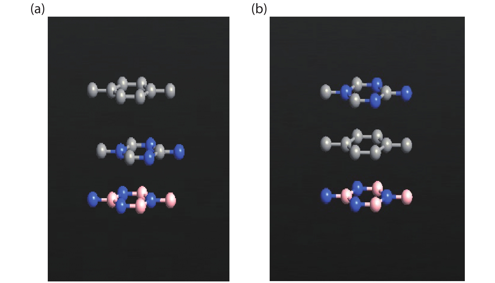
Fig. 1.  (Color online) Proposed heterostructures (a) G/g-C3N4/h-BN in ABA stack and (b) g-C3N4/G/h-BN in AAA stack.

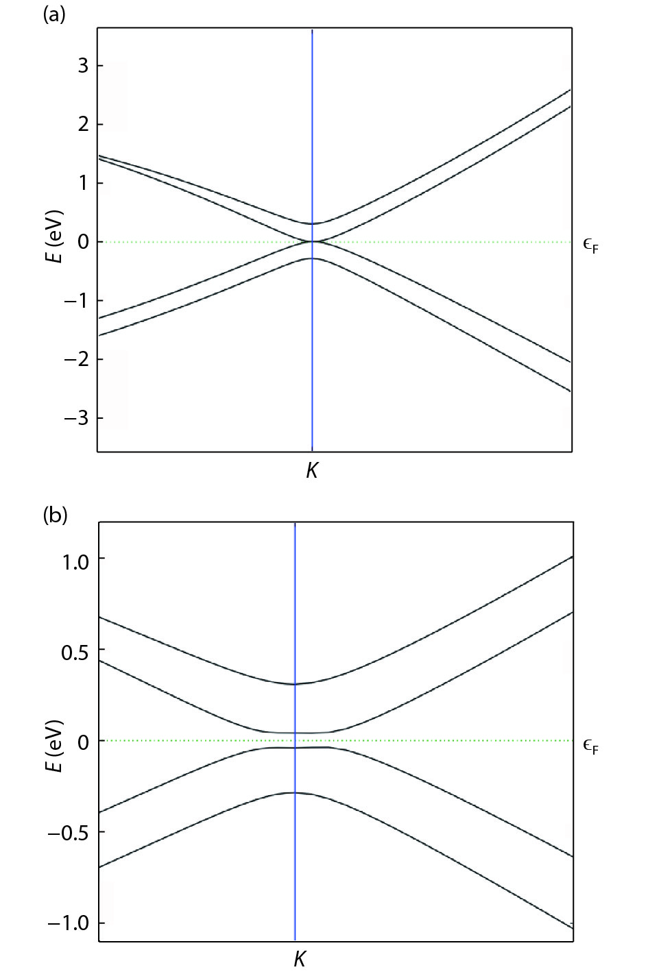
Fig. 2.  (Color online) Band structure of BLG in Bernal (AB) stack at (a) 0 and (b) 4 V/nm.

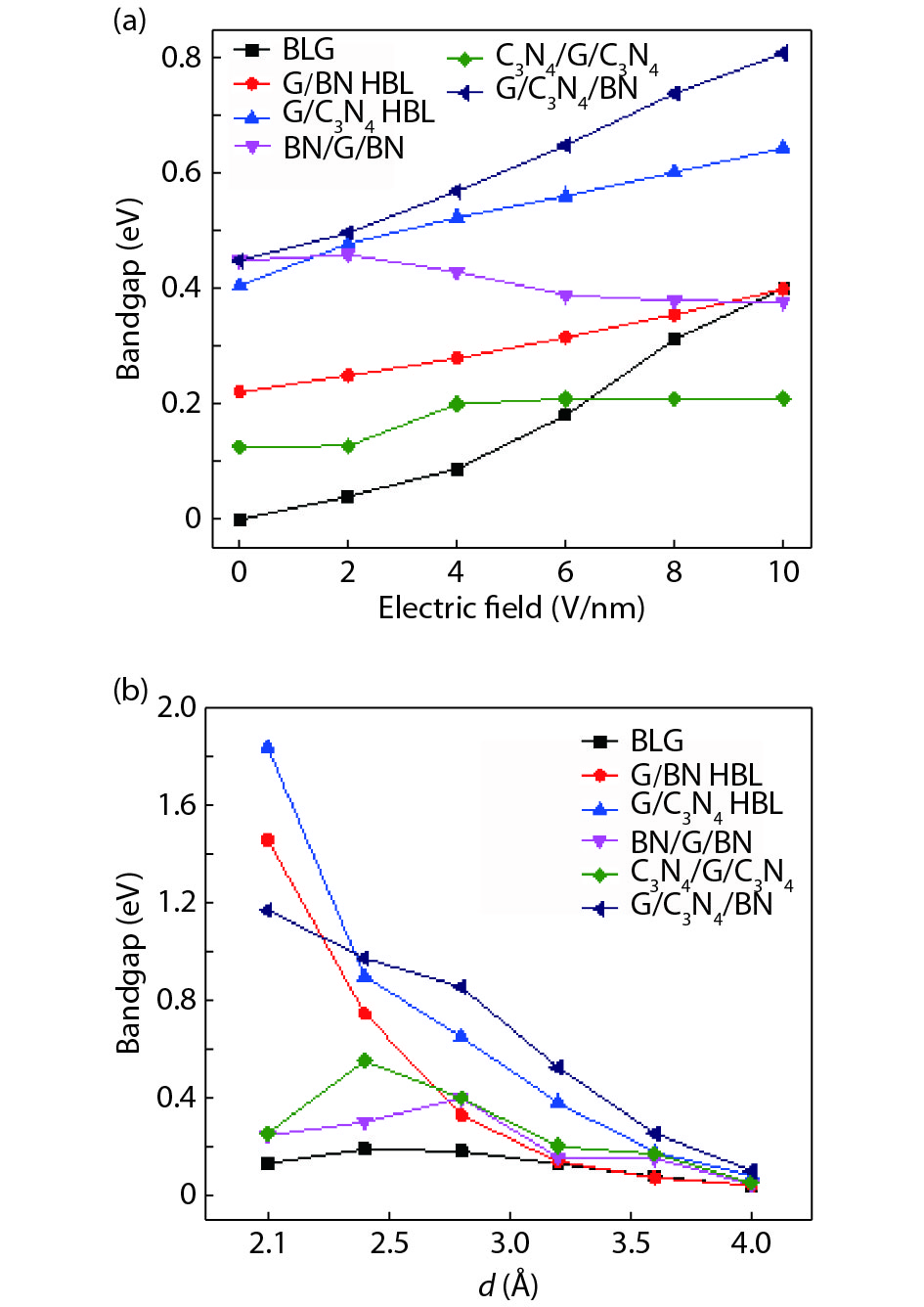
Fig. 3.  (Color online) Bandgap in Bernal stack w.r.t. (a) Electric field (E) keeping interlayer distance d1 = d2 = 2.8 Å and (b) interlayer distance (keeping d1 = d2) and E = 6 V/nm.

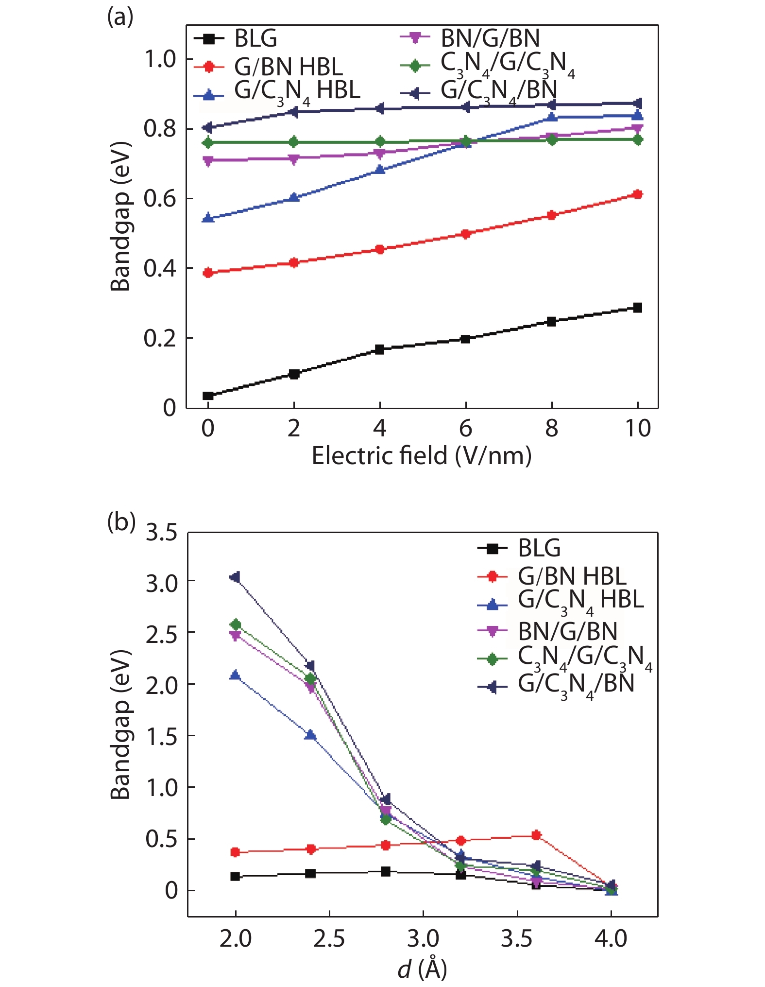
Fig. 4.  (Color online) Bandgap in hexagonal stack w.r.t. (a) Electric field (E) keeping interlayer distance d1 = d2 = 2.8 Å and (b) interlayer distance (keeping d1 = d2) and E = 6 V/nm.

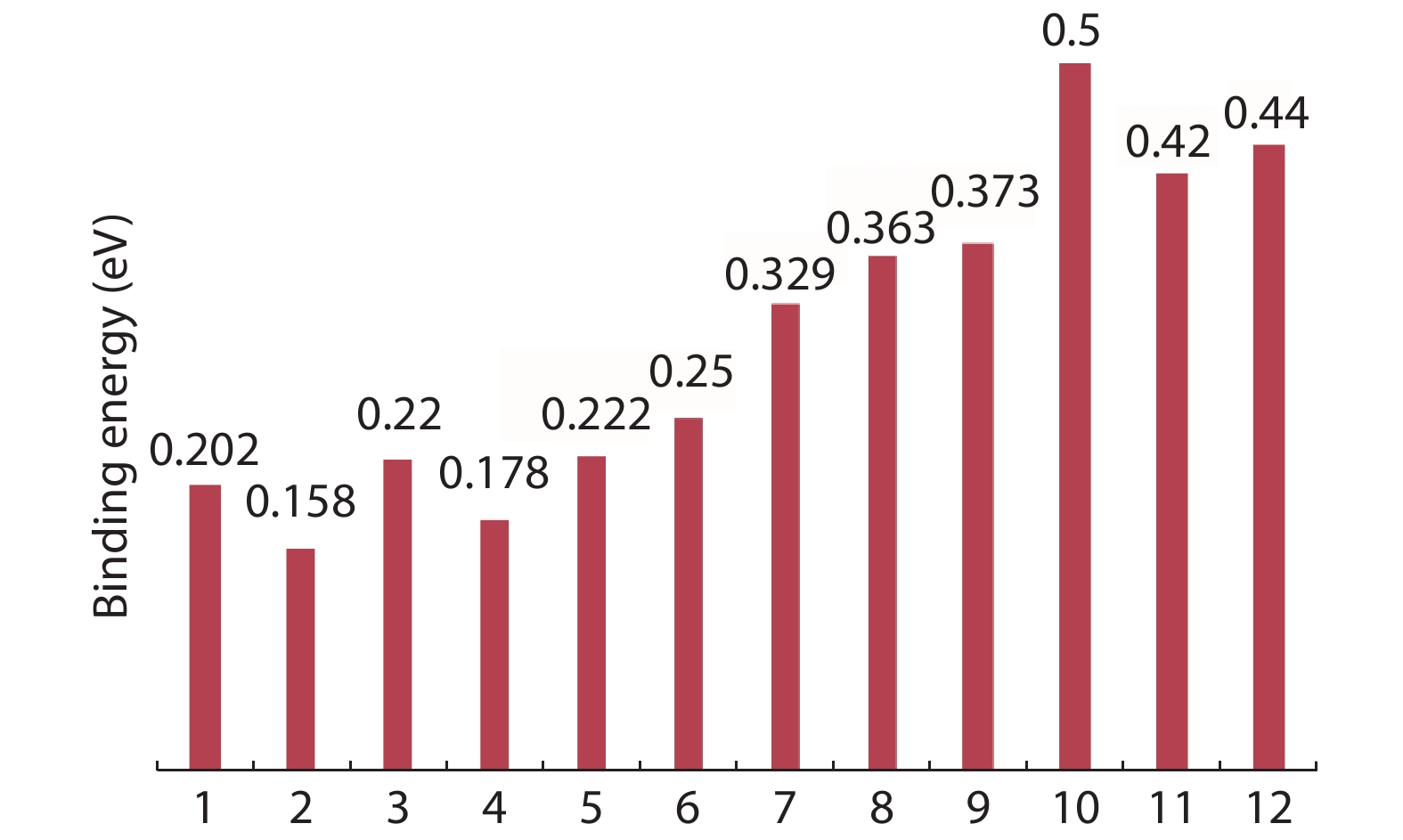
Fig. 5.  (Color online) Binding energies for (1) GBL -AB stack, (2) GBL-AA, (3) G/BN-AB, (4) G/BN-AA, (5) G/C3N4-AB, (6) G/C3N4-AA, (7) BN/G/BN-AB, (8) BN/G/BN-AA, (9) C3N4/G/C3N4-ABA, (10) C3N4/G/C3N4-AAA, (11) G/C3N4/BN- ABA, and (12) C3N4/G/BN-AAA.

Table 1.   Interlayer distance in Bernal stack.

Graphene structure Inter atomic distance (Å)
at 0 V/nm at 6 V/nm
d1 d2 d1 d2
BLG[9] 3.157 3.138
G/BN[23] 3.129 3.122
G/C3N4[13] 3.108 3.056
BN/G/BN[24] 3.265 3.265 3.292 3.258
C3N4/G/C3N4[14] 3.107 3.110 3.132 3.119
G/C3N4/BN 3.239 3.126 3.173 3.100
DownLoad: CSV

Table 2.   Interlayer distance in hexagonal stack.

Graphene structure Inter atomic distance (Å)
at 0 V/nm at 6 V/nm
d1 d2 d1 d2
BLG[9] 3.367 3.282
G/BN[23] 3.320 3.279
G/C3N4[13] 3.108 3.056
BN/G/BN[24] 3.297 3.295 3.292 3.258
C3N4/G/C3N4[14] 3.0 3.0 3.094 2.982
C3N4/G/BN 3.294 3.004 3.295 3.05
DownLoad: CSV

Table 3.   Binding energies (Eb) for different heterostructures.

Graphene structure Binding energies (Eb)
BLG \small$E_{\rm graphene}-nE_{\rm C}$
G/BN $E_{\rm heterostructure}-E_{\rm G}-E_{\rm BN}$
G/C3N4 ${E_{\rm heterostructure}-{E_{\rm G}}-{E_{{\rm C_3}{\rm N_4}}}}$
BN/G/BN $E_{\rm heterostructure}-E_{\rm G}-2 E_{\rm BN}$
C3N4/G/C3N4 $E_{\rm heterostructure}-{E_{\rm G}}-2 E_{{\rm C_3}{\rm N_4}}$
G/C3N4/BN $E_{\rm heterostructure}-{E_G}-E_{\rm BN}-E_{{\rm C_3}{\rm N_4}}$
C3N4/G/BN $E_{\rm heterostructure}-E_{\rm G}-E_{\rm BN}-E_{{\rm C_3}{\rm N_4}}$
DownLoad: CSV

Table 4.   Effective mass at 6 V/nm field with interlayer distance (both d1 and d2) fixed at 2.8 Å.

Graphene structure Bernal stack Hexagonal stack
Electron Hole Electron Hole
BLG 0.300 0.335 0.436 0.527
G/BN 0.315 0.366 0.294 0.372
G/C3N4 0.286 0.324 0.268 0.349
BN/G/BN 0.316 0.471 0.360 0.390
C3N4/G/C3N4 0.335 0.347 0.345 0.371
G/C3N4/BN 0.354 0.415
C3N4/G/BN 0.274 0.346
DownLoad: CSV
[1]
Geim A K, Novoselov K S. The rise of graphene. Nat Mater, 2007, 6: 183 doi: 10.1038/nmat1849
[2]
Gupta M, Gaur N, Kumar P, et al. Tailoring the electronic properties of a Z-shaped graphene field effect transistor via B/N doping. Phys Lett A, 2015, 379: 710 doi: 10.1016/j.physleta.2014.12.046
[3]
Novoselov K S, Geim A K, Morozov S. Electric field effect in atomically thin carbon films. Science, 2004, 306: 666 doi: 10.1126/science.1102896
[4]
Wang X R, Ouyang Y J, Li X L, et al. Room-temperature all semiconducting sub-10-nm Graphene nanoribbon field-effect transistors. Phys Rev Lett, 2008, 100: 206803 doi: 10.1103/PhysRevLett.100.206803
[5]
Giovannetti G, Khomyakov P A, Brocks G, et al. Substrate induced band gap in Graphene on hexagonal boron nitride: Ab initio density functional calculations. Phys Rev B, 2007, 76: 073103 doi: 10.1103/PhysRevB.76.073103
[6]
Ao Z M, Peeters F M. electric field activated hydrogen dissociative adsorption to nitrogen-doped graphene. J Phys Chem C, 2010, 114(34): 14503 doi: 10.1021/jp103835k
[7]
Zhou J, Wu M M, Zhou X, et al. Tuning electronic and magnetic properties of Graphene by surface modification. Appl Phys Lett, 2009, 95: 103108 doi: 10.1063/1.3225154
[8]
Choi S M, Jhi S H, Son Y W. Effects of strain on electronic properties of Graphene. Phys Rev B, 2010, 81: 081407 doi: 10.1103/PhysRevB.81.081407
[9]
Zhang Y, Tang T T, Girit C, et al. Direct observation of a widely tunable bandgap in bilayer graphene. Nature, 2009, 459: 820 doi: 10.1038/nature08105
[10]
Tao W, Qing G, Yan L, et al. A comparative investigation of an AB- and AA-stacked bilayer Graphene sheet under an applied electric field: A density functional theory study. Chin Phys B, 2012, 21(6): 067301 doi: 10.1088/1674-1056/21/6/067301
[11]
Avetisyan A A, Partoens B, Peeters F M. Stacking order dependent electric field tuning of the band gap in Graphene multilayers. Phys Rev B, 2010, 81: 115432 doi: 10.1103/PhysRevB.81.115432
[12]
Zhu J, Xiao P, Li H, et al. Graphitic Carbon Nitride: Synthesis, Properties, and Applications in Catalysis. ACS Appl Mater Interf, 2014, 6: 16449 doi: 10.1021/am502925j
[13]
Li X R, Dai Y, Ma Y D, et al. Graphene/g-C3N4 bilayer: considerable band gap opening and effective band structure engineering. Phys Chem Chem Phys, 2014, 16: 4230 doi: 10.1039/c3cp54592j
[14]
Dong M M, He C, Zhang W X, et al. Tunable and sizable bandgap of g-C3N4/Graphene/g-C3N4 sandwich heterostructure: a Van Der Waals density functional study. J Mater Chem C, 2017, 5: 3830 doi: 10.1039/C7TC00386B
[15]
Hu Wei, Li Zhenyu, Yang Jinlong. Structural, electronic, and optical properties of hybrid silicene and graphene nanocomposite. J Chem Phys, 2013, 139: 154704 doi: 10.1063/1.4824887
[16]
Atomistix Toolkit version 2017.1, Synopsys Quantum Wise A/S (www.quantumwise.com)
[17]
Smidstrup S, et al. First-principles Green's-function method for surface calculations: A pseudopotential localized basis set approach. Phys Rev B, 2017, 96: 195309 doi: 10.1103/PhysRevB.96.195309
[18]
Schlipf M, Gygi F. Optimization algorithm for the generation of ONCV pseudopotentials. Comp Phys Commun, 2015, 196: 36 doi: 10.1016/j.cpc.2015.05.011
[19]
Setten M J van, et al. The PseudoDojo: Training and grading a 85 element optimized norm-conserving pseudopotential table. Comp Phys Comm, 2018, 226: 39-54 doi: 10.1016/j.cpc.2018.01.012
[20]
Stokbro K, et al. Semiempirical model for nanoscale device simulations, Phys Rev B, 2010, 82: 075420 doi: 10.1103/PhysRevB.82.075420
[21]
Pulay P. Convergence acceleration of iterative sequences, The case of SCF iteration. Chem Phys Lett, 1980, 73(2): 393 doi: 10.1016/0009-2614(80)80396-4
[22]
Wang J, Ma F, Sun M. Graphene, hexagonal boron nitride, and their heterostructures: properties and applications. RSC Adv, 2017, 7, 16801 doi: 10.1039/C7RA00260B
[23]
Ghosh R K, Mahapatra S. Proposal for Graphene-Boron Nitride Heterobilayer Based Tunnel FET. IEEE Trans Nanotechnol, 2013, 12(5): 665 doi: 10.1109/TNANO.2013.2272739
[24]
Ramasubramaniam A, Naveh D, Towe E. Tunable band gaps in bilayer Graphene/h-BN heterostructures. Nano Lett, 2011, 11: 1070 doi: 10.1021/nl1039499
  • Search

    Advanced Search >>

    GET CITATION

    shu

    Export: BibTex EndNote

    Article Metrics

    Article views: 4076 Times PDF downloads: 66 Times Cited by: 0 Times

    History

    Received: 25 March 2018 Revised: 06 August 2018 Online: Accepted Manuscript: 05 January 2019Uncorrected proof: 09 January 2019Published: 01 March 2019

    Catalog

      Email This Article

      User name:
      Email:*请输入正确邮箱
      Code:*验证码错误
      Santosh Kumar Gupta, Rupesh Shukla. Bandgap engineered novel g-C3N4/G/h-BN heterostructure for electronic applications[J]. Journal of Semiconductors, 2019, 40(3): 032801. doi: 10.1088/1674-4926/40/3/032801 ****S K Gupta, R Shukla, Bandgap engineered novel g-C3N4/G/h-BN heterostructure for electronic applications[J]. J. Semicond., 2019, 40(3): 032801. doi: 10.1088/1674-4926/40/3/032801.
      Citation:
      Santosh Kumar Gupta, Rupesh Shukla. Bandgap engineered novel g-C3N4/G/h-BN heterostructure for electronic applications[J]. Journal of Semiconductors, 2019, 40(3): 032801. doi: 10.1088/1674-4926/40/3/032801 ****
      S K Gupta, R Shukla, Bandgap engineered novel g-C3N4/G/h-BN heterostructure for electronic applications[J]. J. Semicond., 2019, 40(3): 032801. doi: 10.1088/1674-4926/40/3/032801.

      Bandgap engineered novel g-C3N4/G/h-BN heterostructure for electronic applications

      DOI: 10.1088/1674-4926/40/3/032801
      More Information

      Catalog

        /

        DownLoad:  Full-Size Img  PowerPoint
        Return
        Return