J. Semicond. > 2019, Volume 40 > Issue 4 > 041901

REVIEWS

Recent progress of the optoelectronic properties of 2D Ruddlesden-Popper perovskites

Haizhen Wang1, 2, Chen Fang1, Hongmei Luo2, and Dehui Li1,

+ Author Affiliations

 Corresponding author: Hongmei Luo, Email: hluo@nmsu.edu; Dehui Li, Email: dehuili@hust.edu.cn

DOI: 10.1088/1674-4926/40/4/041901

PDF

Turn off MathJax

Abstract: Two-dimensional (2D) hybrid organic-inorganic perovskites have recently attracted attention due to their layered nature, naturally formed quantum well structure, large exciton binding energy and especially better long-term environmental stability compared with their three-dimensional (3D) counterparts. In this report, we present a brief overview of the recent progress of the optoelectronic applications in 2D perovskites. The layer number dependent physical properties of 2D perovskites will first be introduced and then the different synthetic approaches to achieve 2D perovskites with different morphologies will be discussed. The optical, optoelectronic properties and self-trapped states in 2D perovskites will be described, which are indispensable for designing the new device structures with novel functionalities and improving the device performance. Subsequently, a brief summary of the advantages and the current research status of the 2D perovskite-based heterostructures will be illustrated. Finally, a perspective of 2D perovskite materials is given toward their material synthesis and novel device applications.

Key words: 2D perovskiteoptoelectronicsself-trapped excitonheterostructures


[1]
Moure C, Peña O. Recent advances in perovskites: processing and properties. Prog Solid State Chem, 2015, 43, 123 doi: 10.1016/j.progsolidstchem.2015.09.001
[2]
Mtougui S, Khalladi R, Ziti S, et al. Magnetic properties of the perovskite BiFeO3: Monte Carlo simulation. Superlattice Microstruct, 2018, 123, 111 doi: 10.1016/j.spmi.2018.05.005
[3]
Li C, Lu X, Ding W, et al. Formability of ABX3 (X = F, Cl, Br, I) halide perovskites. Acta Crystallograph B, 2008, 64, 702 doi: 10.1107/S0108768108032734
[4]
Bhalla A S, Guo R, Roy R. The perovskite structure—a review of its role in ceramic science and technology. Mater Res Innov, 2016, 4, 3
[5]
Li W, Wang Z, Deschler F, et al. Chemically diverse and multifunctional hybrid organic–inorganic perovskites. Nat Rev Mater, 2017, 2, 16099 doi: 10.1038/natrevmats.2016.99
[6]
Saparov B, Mitzi D. Organic–inorganic perovskites: structural versatility for functional materials design. Chem Rev, 2016, 116, 4558 doi: 10.1021/acs.chemrev.5b00715
[7]
Brenner T M, Egger D A, Kronik L, et al. Hybrid organic–inorganic perovskites: low-cost semiconductors with intriguing charge-transport properties. Nat Rev Mater, 2016, 1, 15007 doi: 10.1038/natrevmats.2015.7
[8]
Weber D. Das Perowskitsystem CH3NH3[Pb, Sn1-nX3] (X = Cl, Br, I)/The perovskite system CH3NH3[PbnSn1-nX3]. Zeitschrift fr Naturforschung B, 1979
[9]
Snaith H J. Perovskites: the emergence of a new era for low-cost, high-efficiency solar cells. J Am Chem Soc, 2013, 4, 3623
[10]
Grätzel M. The light and shade of perovskite solar cells. Nat Mater, 2014, 13, 838 doi: 10.1038/nmat4065
[11]
Kojima A, Teshima K, Shirai Y, et al. Organometal halide perovskites as visible-light sensitizers for photovoltaic cells. J Am Chem Soc, 2009, 131, 6050 doi: 10.1021/ja809598r
[12]
Shi D, Adinolfi V, Comin R, et al. Low trap-state density and long carrier diffusion in organolead trihalide perovskite single crystals. Science, 2015, 347, 519 doi: 10.1126/science.aaa2725
[13]
Shaikh J S, Shaikh N S, Sheikh A D, et al. Perovskite solar cells: In pursuit of efficiency and stability. Mater Des, 2017, 136, 54 doi: 10.1016/j.matdes.2017.09.037
[14]
Johnston M B, Herz L M. Hybrid perovskites for photovoltaics: charge-carrier recombination, diffusion, and radiative efficiencies. Accounts Chem Res, 2015, 49, 146
[15]
NREL Best research-cell efficiencies. https://www.nrel.gov/pv/assets/images/efficiency-chart-20180716.jpg (accessed 16 July 2018).
[16]
Bush K A, Manzoor S, Frohna K, et al. Minimizing current and voltage losses to reach 25% efficient monolithic two-terminal perovskite–silicon tandem solar cells. ACS Energy Lett, 2018, 3, 2173 doi: 10.1021/acsenergylett.8b01201
[17]
Wangyang P, Gong C, Rao G, et al. Recent advances in halide perovskite photodetectors based on different dimensional materials. Adv Opt Mater, 2018, 6, 1701302 doi: 10.1002/adom.v6.11
[18]
Shen L, Fang Y, Wang D, et al. A self-powered, sub-nanosecond-response solution-processed hybrid perovskite photodetector for time-resolved photoluminescence-lifetime detection. Adv Mater, 2016, 28, 10794 doi: 10.1002/adma.201603573
[19]
Dong R, Fang Y, Chae J, et al. High-gain and low-driving-voltage photodetectors based on organolead triiodide perovskites. Adv Mater, 2015, 27, 1912 doi: 10.1002/adma.v27.11
[20]
Fang Y, Dong Q, Shao Y, et al. Highly narrowband perovskite single-crystal photodetectors enabled by surface-charge recombination. Nat Photon, 2015, 9, 679 doi: 10.1038/nphoton.2015.156
[21]
Xing G, Mathews N, Lim S S, et al. Low-temperature solution-processed wavelength tunable perovskites for lasing. Nat Mater, 2014, 13, 476 doi: 10.1038/nmat3911
[22]
Yuan Z, Zhou C, Tian Y, et al. One-dimensional organic lead halide perovskites with efficient bluish white-light emission. Nat Commun, 2017, 8, 14051 doi: 10.1038/ncomms14051
[23]
Niu G, Guo X, Wang L. Review of recent progress in chemical stability of perovskite solar cells. J Mater Chem, A, 2015, 3, 8970 doi: 10.1039/C4TA04994B
[24]
Rong Y, Liu L, Mei A, et al. Beyond efficiency: the challenge of stability in mesoscopic perovskite solar cells. Adv Energy Mater, 2015, 5, 1501066 doi: 10.1002/aenm.201501066
[25]
Turren-Cruz S H, Saliba M, Mayer M T, et al. Enhanced charge carrier mobility and lifetime suppress hysteresis and improve efficiency in planar perovskite solar cells. Energy Environ Sci, 2018, 11, 78 doi: 10.1039/C7EE02901B
[26]
Babayigit A, Ethirajan A, Muller M, et al. Toxicity of organometal halide perovskite solar cells. Nat Mater, 2016, 15, 247 doi: 10.1038/nmat4572
[27]
Snaith H J, Abate A, Ball J M, et al. Anomalous hysteresis in perovskite solar cells. J Phys Chem Lett, 2014, 5, 1511 doi: 10.1021/jz500113x
[28]
Tress W, Marinova N, Moehl T, et al. Understanding the rate-dependent J–V hysteresis, slow time component, and aging in CH3NH3PbI3 perovskite solar cells: the role of a compensated electric field. Energy Environ Sci, 2015, 8, 995 doi: 10.1039/C4EE03664F
[29]
Sutton R J, Eperon G E, Miranda L, et al. Bandgap-tunable cesium lead halide perovskites with high thermal stability for efficient solar cells. Adv Energy Mater, 2016, 6, 1502458 doi: 10.1002/aenm.201502458
[30]
Conings B, Drijkoningen J, Gauquelin N, et al. Intrinsic thermal instability of methylammonium lead trihalide perovskite. Adv Energy Mater, 2015, 5, 1500477 doi: 10.1002/aenm.201500477
[31]
Nie W, Blancon J C, Neukirch A J, et al. Light-activated photocurrent degradation and self-healing in perovskite solar cells. Nat Commun, 2016, 7, 11574 doi: 10.1038/ncomms11574
[32]
Smith I C, Hoke E T, Solis-Ibarra D, et al. A layered hybrid perovskite solar-cell absorber with enhanced moisture stability. Angew Chem, 2014, 53, 11232 doi: 10.1002/anie.201406466
[33]
Chen Y, Sun Y, Peng J, et al. 2D Ruddlesden-Popper perovskites for optoelectronics. Adv Mater, 2018, 30, 1703487 doi: 10.1002/adma.v30.2
[34]
Pedesseau L, Sapori D, Traore B, et al. Advances and promises of layered halide hybrid perovskite semiconductors. ACS Nano, 2016, 10, 9776 doi: 10.1021/acsnano.6b05944
[35]
Stoumpos C C, Cao D H, Clark D J, et al. Ruddlesden–Popper hybrid lead iodide perovskite 2D homologous semiconductors. Chem Mater, 2016, 28, 2852 doi: 10.1021/acs.chemmater.6b00847
[36]
Shen H, Li J, Wang H, et al. Two-dimensional lead-free perovskite (C6H5C2H4NH3)2CsSn2I7 with high hole mobility. J Phys Chem Lett, 2018, 10, 7 doi: 10.1021/acs.jpclett.8b03381
[37]
Soe C, Stoumpos C, Kepenekian M, et al. New type of 2D perovskites with alternating cations in the interlayer space, (C(NH2)3)(CH3NH3)nPbnI3n+1: Structure, properties, and photovoltaic performance. J Am Chem Soc, 2017, 139, 16297 doi: 10.1021/jacs.7b09096
[38]
Li J, Wang J, Zhang Y, et al. Fabrication of single phase 2D homologous perovskite microplates by mechanical exfoliation. 2D Mater, 2018, 5, 021001 doi: 10.1088/2053-1583/aaa5d4
[39]
Straus D, Iotov N, Gau M, et al. Longer cations increase energetic disorder in excitonic 2D hybrid perovskites. J Phys Chem Lett, 2019, 10, 1198 doi: 10.1021/acs.jpclett.9b00247
[40]
Cao D H, Stoumpos C C, Farha O K, et al. 2D homologous perovskites as light-absorbing materials for solar cell applications. J Am Chem Soc, 2015, 137, 7843 doi: 10.1021/jacs.5b03796
[41]
Gauthron K, Lauret J, Doyennette L, et al. Optical spectroscopy of two-dimensional layered (C6H5C2H4–NH3)2–PbI4 perovskite. Opt Express, 2010, 18, 5912 doi: 10.1364/OE.18.005912
[42]
Tan Z, Wu Y, Hong H, et al. Two-dimensional (C4H9NH3)2PbBr4 perovskite crystals for high-performance photodetector. J Am Chem Soc, 2016, 138, 16612 doi: 10.1021/jacs.6b11683
[43]
Quan L N, Zhao Y, Garcia de Arquer F P, et al. Tailoring the energy landscape in quasi-2D halide perovskites enables efficient green-light emission. Nano Lett, 2017, 17, 3701 doi: 10.1021/acs.nanolett.7b00976
[44]
Matsushima T, Mathevet F, Heinrich B, et al. N-channel field-effect transistors with an organic–inorganic layered perovskite semiconductor. Appl Phys Lett, 2016, 109, 253301 doi: 10.1063/1.4972404
[45]
Matsushima T, Hwang S, Sandanayaka A S, et al. Solution-processed organic-inorganic perovskite field-effect transistors with high hole mobilities. Adv Mater, 2016, 28, 10275 doi: 10.1002/adma.201603126
[46]
Wang J, Shen H, Li W, et al. The role of chloride incorporation in lead-free 2D perovskite (BA)2SnI4: morphology, photoluminescence, phase transition, and charge transport, and charge transport. Adv Sci, 2019, 1802019 doi: 10.1002/advs.201802019
[47]
Milot R L, Sutton R J, Eperon G E, et al. Charge-carrier dynamics in 2D hybrid metal–halide perovskites. Nano Lett, 2016, 16, 7001 doi: 10.1021/acs.nanolett.6b03114
[48]
Kumagai M, Takagahara T. Excitonic and nonlinear-optical properties of dielectric quantum-well structures. Phys Rev B, 1989, 40, 12359 doi: 10.1103/PhysRevB.40.12359
[49]
Hong X, Ishihara T, Nurmikko A. Dielectric confinement effect on excitons in PbI4-based layered semiconductors. Phys Rev B, 1992, 45, 6961 doi: 10.1103/PhysRevB.45.6961
[50]
Quan L N, Yuan M, Comin R, et al. Ligand-stabilized reduced-dimensionality perovskites. J Am Chem Soc, 2016, 138, 2649 doi: 10.1021/jacs.5b11740
[51]
Liu B, Long M, Cai M Q, et al. Influence of the number of layers on ultrathin CsSnI3 perovskite: from electronic structure to carrier mobility. J Phys D, 2018, 51, 105101 doi: 10.1088/1361-6463/aaa7ca
[52]
Tsai H, Nie W, Blancon J C, et al. High-efficiency two-dimensional Ruddlesden-Popper perovskite solar cells. Nature, 2016, 536, 312 doi: 10.1038/nature18306
[53]
Fang C, Wang H, Shen Z, et al. High-performance photodetectors based on lead-free 2D Ruddlesden-Popper perovskite/MoS2 heterostructures. ACS Appl Mater Interfaces, 2019, 11(8419) doi: 10.1021/acsami.8b20538
[54]
Misra R K, Cohen B E, Iagher L, et al. Low-dimensional organic–inorganic halide perovskite: structure, properties, and applications. ChemSusChem, 2017, 10, 3712 doi: 10.1002/cssc.v10.19
[55]
Even J, Pedesseau L, Katan C. Understanding quantum confinement of charge carriers in layered 2D hybrid perovskites. ChemPhysChem, 2014, 15, 3733 doi: 10.1002/cphc.v15.17
[56]
Grancini G, Roldán-Carmona C, Zimmermann I, et al. One-year stable perovskite solar cells by 2D/3D interface engineering. Nat Commun, 2017, 8, 15684 doi: 10.1038/ncomms15684
[57]
Wang Z, Lin Q, Chmiel F P, et al. Efficient ambient-air-stable solar cells with 2D–3D heterostructured butylammonium-caesium-formamidinium lead halide perovskites. Nat Energy, 2017, 2, 17135 doi: 10.1038/nenergy.2017.135
[58]
Yan J, Qiu W, Wu G, et al. Recent progress on 2D/quasi-2D layered metal halide perovskites for solar cells. J Mater Chem A, 2018, 6, 11063 doi: 10.1039/C8TA02288G
[59]
Bai Y, Xiao S, Hu C, et al. Dimensional engineering of a graded 3D–2D halide perovskite interface enables ultrahigh Voc enhanced stability in the p–i–n photovoltaics. Adv Energy Mater, 2017, 7, 1701038 doi: 10.1002/aenm.201701038
[60]
Yuan M, Quan L N, Comin R, et al. Perovskite energy funnels for efficient light-emitting diodes. Nat Nanotechnol, 2016, 11, 872 doi: 10.1038/nnano.2016.110
[61]
Koh T M, Shanmugam V, Schlipf J, et al. Nanostructuring mixed-dimensional perovskites: a route toward tunable, efficient photovoltaics. Adv Mater, 2016, 28, 3653 doi: 10.1002/adma.201506141
[62]
Wang J, Li J, Lan S, et al. Controllable growth of centimeter-size 2D perovskite heterostructural single crystals for highly narrow dual-band photodetectors. arXiv preprint arXiv: 1807.02807, 2018
[63]
Zhou J, Chu Y, Huang J. Photodetectors based on two-dimensional layer-structured hybrid lead iodide perovskite semiconductors. ACS Appl Mater Interfaces, 2016, 8, 25660 doi: 10.1021/acsami.6b09489
[64]
Wang N, Cheng L, Ge R, et al. Perovskite light-emitting diodes based on solution-processed self-organized multiple quantum wells. Nat Photon, 2016, 10, 699 doi: 10.1038/nphoton.2016.185
[65]
Wang Y Y, Gao R X, Ni Z H, et al. Thickness identification of two-dimensional materials by optical imaging. Nanotechnology, 2012, 23, 495713 doi: 10.1088/0957-4484/23/49/495713
[66]
Chen J, Gan L, Zhuge F, et al. A ternary solvent method for large-sized two-dimensional perovskites. Angew Chem, 2017, 129, 2430 doi: 10.1002/ange.201611794
[67]
Dou L, Wong A B, Yu Y, et al. Atomically thin two-dimensional organic-inorganic hybrid perovskites. Science, 2015, 349, 1518 doi: 10.1126/science.aac7660
[68]
Fang C, Li J, Wang J, et al. Controllable growth of two-dimensional perovskite microstructures. CrystEngComm, 2018, 20, 6538 doi: 10.1039/C8CE01087K
[69]
Chen Z, Wang Y, Sun X, et al. Van Der Waals hybrid perovskite of high optical quality by chemical vapor deposition. Adv Opt Mater, 2017, 5, 201700373 doi: 10.1002/adom.201700373
[70]
Li L, Li J, Lan S, et al. Two-step growth of 2D organic-inorganic perovskite microplates and arrays for functional optoelectronics. J Phys Chem Lett, 2018, 9, 4532 doi: 10.1021/acs.jpclett.8b01861
[71]
Lin Y, Bai Y, Fang Y, et al. Suppressed ion migration in low-dimensional perovskites. ACS Energy Lett, 2017, 2, 1571 doi: 10.1021/acsenergylett.7b00442
[72]
Liu J, Leng J, Wu K, et al. Observation of internal photoinduced electron and hole separation in hybrid two-dimentional perovskite films. J Am Chem Soc, 2017, 139, 1432 doi: 10.1021/jacs.6b12581
[73]
Hu T, Smith M D, Dohner E R, et al. Mechanism for broadband white-light emission from two-dimensional (110) hybrid perovskites. J Phys Chem Lett, 2016, 7, 2258 doi: 10.1021/acs.jpclett.6b00793
[74]
Emin D, Holstein T. Adiabatic theory of an electron in a deformable continuum. Phys Rev Lett, 1976, 36, 323 doi: 10.1103/PhysRevLett.36.323
[75]
Kabanov V V, Mashtakov O Y. Electron localization with and without barrier formation. Phys Rev B, 1993, 47, 6060 doi: 10.1103/PhysRevB.47.6060
[76]
Smith M D, Jaffe A, Dohner E R, et al. Structural origins of broadband emission from layered Pb–Br hybrid perovskites. Chem Sci, 2017, 8, 4497 doi: 10.1039/C7SC01590A
[77]
Yangui A, Garrot D, Lauret J S, et al. Optical investigation of broadband white-light emission in self-assembled organic–inorganic perovskite (C6H11NH3)2PbBr4. J Phys Chem C, 2015, 119, 23638 doi: 10.1021/acs.jpcc.5b06211
[78]
Li J, Wang J, Ma J, et al. Self-trapped state enabled filterless narrowband photodetections in 2D layered perovskite single crystals. Nat. Commun, 2019, 10, 806 doi: 10.1038/s41467-019-08768-z
[79]
Cortecchia D, Neutzner S, Kandada A R S, et al. Broadband emission in two-dimensional hybrid perovskites: The role of structural deformation. J Am Chem Soc, 2016, 139, 39
[80]
Wu X, Trinh M T, Niesner D, et al. Trap states in lead iodide perovskites. J Am Chem Soc, 2015, 137, 2089 doi: 10.1021/ja512833n
[81]
Straus D B, Parra S H, Iotov N, et al. Direct observation of electron–phonon coupling and slow vibrational relaxation in organic–inorganic hybrid perovskites. J Am Chem Soc, 2016, 138, 13798 doi: 10.1021/jacs.6b08175
[82]
Fu Y, Zheng W, Wang X, et al. Multicolor heterostructures of two-dimensional layered halide perovskites that show interlayer energy transfer. J Am Chem Soc, 2018, 140, 15675 doi: 10.1021/jacs.8b07843
[83]
Hwang B, Lee J S. 2D Perovskite-based self-aligned lateral heterostructure photodetectors utilizing vapor deposition. Adv Opt Mater, 2018 doi: 10.1002/adom.201801356
[84]
Wang J, Li J, Tan Q, et al. Controllable synthesis of two-dimensional Ruddlesden-Popper-type perovskite heterostructures. J Phys Chem Lett, 2017, 8, 6211 doi: 10.1021/acs.jpclett.7b02843
[85]
Ahn J, Lee E, Tan J, et al. A new class of chiral semiconductors: chiral-organic-molecule-incorporating organic–inorganic hybrid perovskites. Mater Horiz, 2017, 4, 851 doi: 10.1039/C7MH00197E
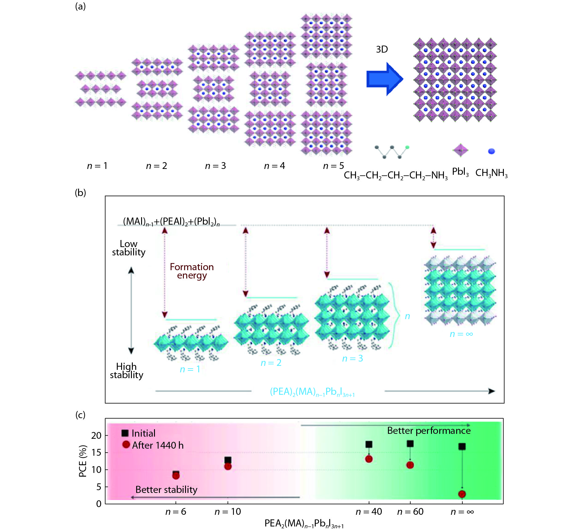
Fig. 1.  (Color online) (a) The schematic illustration of the crystal structures of 2D perovskite (BA)2(MA)n−1PbnI3n+1 for n = 1 to ∞. (b) The structure schematic illustration and stability of 2D perovskite (PEA)2MAn−1PbnI3n+1 for n = 1 to ∞. (c) The layer number n-dependent power conversion efficiency as well as device performance and stability of (PEA)2MAn−1PbnI3n+1. Panel (a) adapted with permission from Ref. [38]. Copyright 2018, Institute of Physics (Great Britain). Panels (b) and (c) adapted with permission from Ref. [50]. Copyright 2016, American Chemical Society.

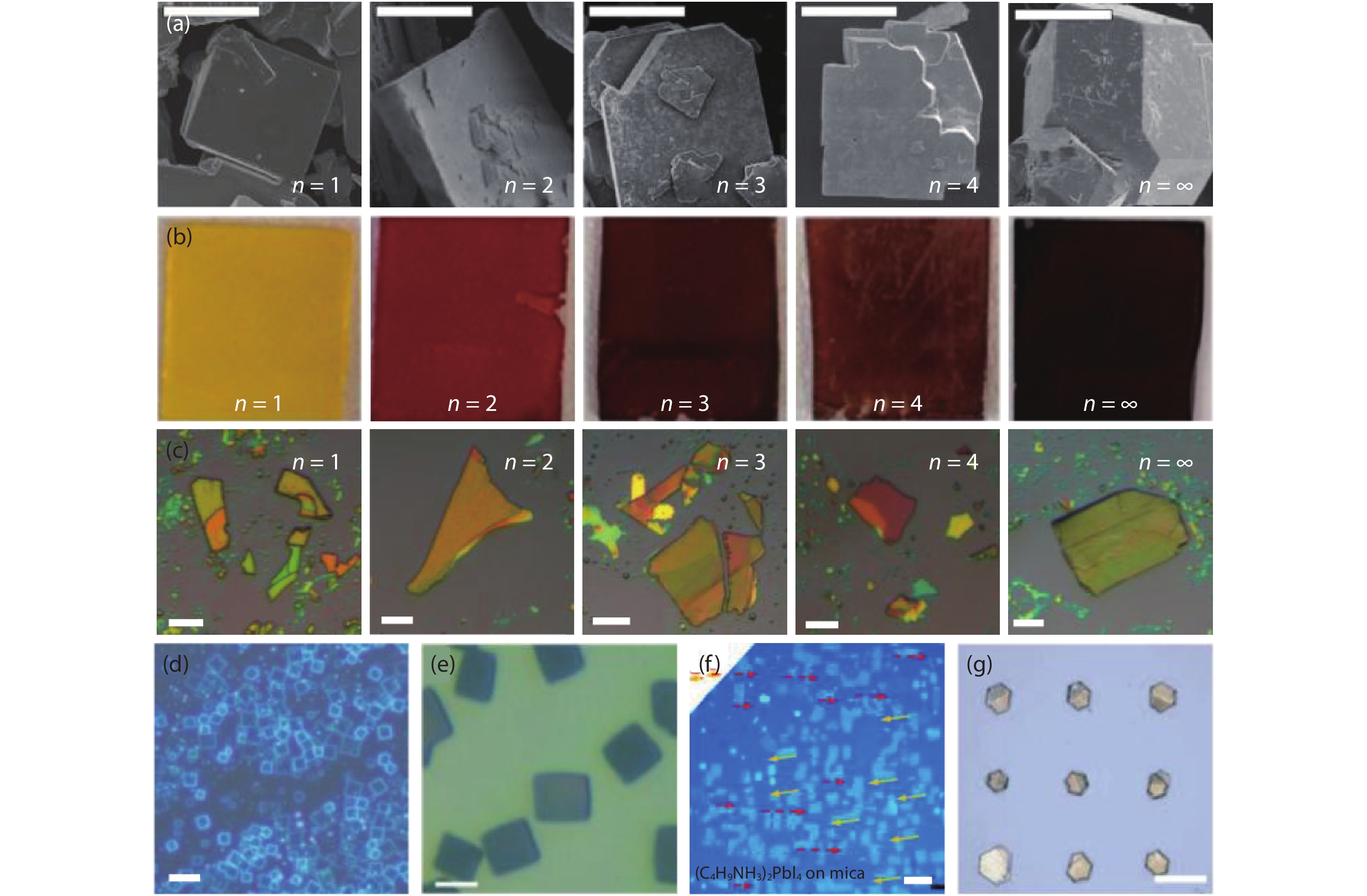
Fig. 2.  (Color online) (a) Scanning electron microscopy (SEM) images of (BA)2(MA)n−1PbnI3n+1 perovskite crystals. The scale bars are 200 μm. (b) Photographs of (BA)2(MA)n−1PbnI3n+1 perovskite films. (c) Optical microscopy (OM) images of the as-exfoliated (BA)2(MA)n−1PbnI3n+1 perovskite microplates. The scale bars are 15 μm. (d) OM image of (BA)2PbBr4 square microplates grown on Si substrate via a solution-phase growth method. The scale bar is 10 μm. (e) OM image of (BA)2(MA)Pb2I7 square plates grown on Si substrate via a spin-coating method. The scale bar is 5 μm. (f) OM image of (BA)2PbI4 flakes grown on mica substrate via a co-evaporation method. The scale bar is 5 μm. (g) OM image of the converted (BA)2Pbl4−xClx microplate array on Si via a vapor phase intercalation method. The scale bar is 20 μm. Panel (a) adapted with permission from Ref. [33]. Copyright 2016, American Chemical Society. Panel (b) adapted with permission from Ref. [40]. Copyright 2015, American Chemical Society. Panel (d) adapted with permission from Ref. [67]. Copyright 2015, The American Association for the Advancement of Science. Panel (e) adapted with permission from Ref. [68]. Copyright 2018, Royal Society of Chemistry (Great Britain). Panel (f) adapted with permission from Ref. [69]. Copyright 2017, John Wiley and Sons. Panel (g) adapted with permission from Ref. [70]. Copyright 2018, American Chemical Society.

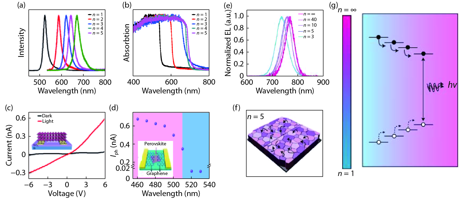
Fig. 3.  (Color online) (a) Normalized PL spectra of the as-exfoliated (BA)2(MA)n−1PbnI3n+1 microplates for n = 1–5 with thickness below 20 nm. (b) Normalized absorption spectra of the as-synthesized (BA)2(MA)n−1PbnI3n+1 plates for n = 1–5. (d) The current–voltage curves of the (BA)2(MA)2Pb3I10 device in dark and under illumination with a 528-nm LED. Inset shows the schematic of the two-probe device. The incident power is 30 μW/cm2. (d) Spectral response of the graphene-(BA)2PbBr4-graphene device under a fixed incident power. The schematic of the as-fabricated device is shown in the inset. (e) Electroluminescence spectra of the (PEA)2MAn−1PbnI3n+1 perovskite films with different n values. (f) Carrier transfer process in (PEA)2MA4Pb5I16 perovskite film. (g) Energy funneling process of (PEA)2MA4Pb5I16 films. Panels (a)–(c) adapted with permission from Ref. [38]. Copyright 2018, Institute of Physics (Great Britain). Panel (d) adapted with permission from Ref. [42]. Copyright 2016, American Chemical Society. Panels (e)–(g) adapted with permission from Ref. [60]. Copyright 2016, Springer Nature.

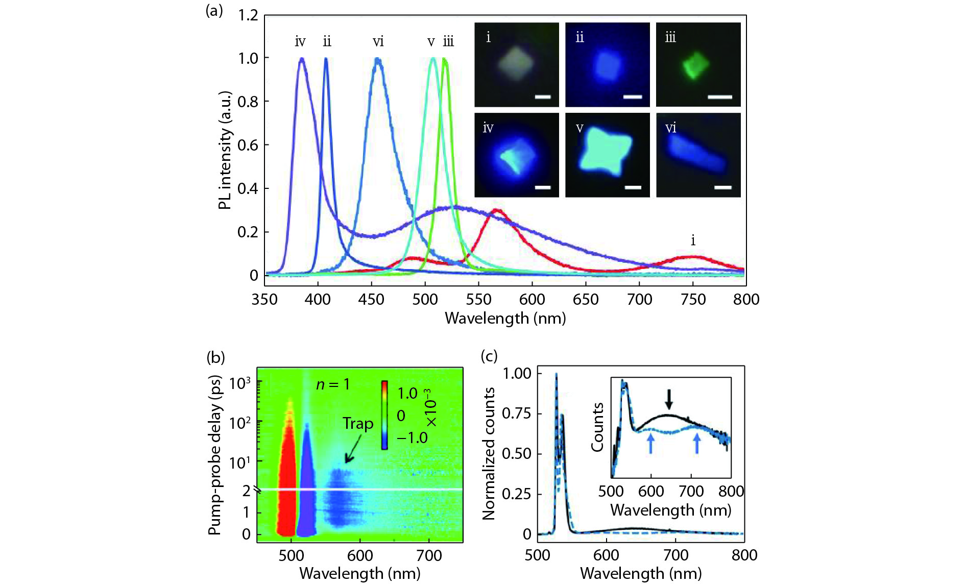
Fig. 4.  (Color online) (a) PL spectra of different 2D hybrid perovskites: (i) (BA)2PbCl4, (ii) (BA)2PbBr4, (iii) (BA)2PbI4, (iv) (BA)2PbCl2Br2, (v) BA)2PbBr2I2 and (vi) (BA)2(MA)Pb2Br7 2D microplates and their corresponding PL images as shown in the inset. The scale bars are 2 μm for (i) to (v) and 10 μm for (vi). (b) Transient absorption spectrum of (BA)2PbI4 at room temperature. (c) PL spectra of the (PEA)2PbI4 thin film and single crystal plotted as black and blue dash line, respectively. The inset shows the spectra on a logarithmic scale. Panel (a) adapted with permission from Ref. [67]. Copyright 2015, The American Association for the Advancement of Science. Panel (b) adapted with permission from Ref. [80]. Copyright 2015, American Chemical Society. Panel (c) adapted with permission from Ref. [81]. Copyright 2016, American Chemical Society.

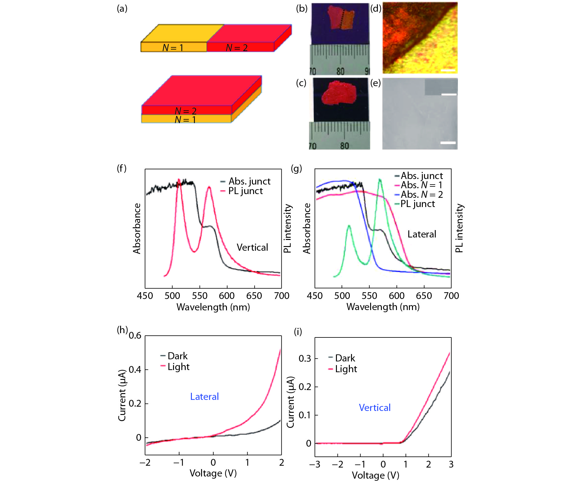
Fig. 5.  (Color online) (a) Schematic illustrations of crystal structure of (BA)2PbI4/(BA)2MAPb2I7 lateral and vertical heterostructures. (b, c) Photographs of the (BA)2PbI4/(BA)2MAPb2I7 lateral and vertical heterostructures, respectively. The boundary of lateral heterostructure are shown in Fig. 5(b) plotted as dotted line, whereas the yellow color portion represents (BA)2PbI4 and the red color portion represents (BA)2MAPb2I7 2D perovskites. (d) OM image of the (BA)2PbI4/(BA)2MAPb2I7 lateral heterostructure. Scale bar: 20 μm. (e) SEM image of (BA)2PbI4/(BA)2MAPb2I7 lateral heterostructure. Scale bar: 30 μm. Inset: the magnified SEM image with a scale bar of 3 μm. (f, g) Normalized absorption and PL spectra of (BA)2PbI4/(BA)2MAPb2I7 vertical and lateral heterostructures, respectively. (h, i) I–V curves of the (BA)2PbI4/(BA)2MAPb2I7 lateral and vertical heterostructure devices in dark and under 1.4 mW/cm2 white light illumination. Adapted with permission from Ref. [84]. Copyright 2017, American Chemical Society.

[1]
Moure C, Peña O. Recent advances in perovskites: processing and properties. Prog Solid State Chem, 2015, 43, 123 doi: 10.1016/j.progsolidstchem.2015.09.001
[2]
Mtougui S, Khalladi R, Ziti S, et al. Magnetic properties of the perovskite BiFeO3: Monte Carlo simulation. Superlattice Microstruct, 2018, 123, 111 doi: 10.1016/j.spmi.2018.05.005
[3]
Li C, Lu X, Ding W, et al. Formability of ABX3 (X = F, Cl, Br, I) halide perovskites. Acta Crystallograph B, 2008, 64, 702 doi: 10.1107/S0108768108032734
[4]
Bhalla A S, Guo R, Roy R. The perovskite structure—a review of its role in ceramic science and technology. Mater Res Innov, 2016, 4, 3
[5]
Li W, Wang Z, Deschler F, et al. Chemically diverse and multifunctional hybrid organic–inorganic perovskites. Nat Rev Mater, 2017, 2, 16099 doi: 10.1038/natrevmats.2016.99
[6]
Saparov B, Mitzi D. Organic–inorganic perovskites: structural versatility for functional materials design. Chem Rev, 2016, 116, 4558 doi: 10.1021/acs.chemrev.5b00715
[7]
Brenner T M, Egger D A, Kronik L, et al. Hybrid organic–inorganic perovskites: low-cost semiconductors with intriguing charge-transport properties. Nat Rev Mater, 2016, 1, 15007 doi: 10.1038/natrevmats.2015.7
[8]
Weber D. Das Perowskitsystem CH3NH3[Pb, Sn1-nX3] (X = Cl, Br, I)/The perovskite system CH3NH3[PbnSn1-nX3]. Zeitschrift fr Naturforschung B, 1979
[9]
Snaith H J. Perovskites: the emergence of a new era for low-cost, high-efficiency solar cells. J Am Chem Soc, 2013, 4, 3623
[10]
Grätzel M. The light and shade of perovskite solar cells. Nat Mater, 2014, 13, 838 doi: 10.1038/nmat4065
[11]
Kojima A, Teshima K, Shirai Y, et al. Organometal halide perovskites as visible-light sensitizers for photovoltaic cells. J Am Chem Soc, 2009, 131, 6050 doi: 10.1021/ja809598r
[12]
Shi D, Adinolfi V, Comin R, et al. Low trap-state density and long carrier diffusion in organolead trihalide perovskite single crystals. Science, 2015, 347, 519 doi: 10.1126/science.aaa2725
[13]
Shaikh J S, Shaikh N S, Sheikh A D, et al. Perovskite solar cells: In pursuit of efficiency and stability. Mater Des, 2017, 136, 54 doi: 10.1016/j.matdes.2017.09.037
[14]
Johnston M B, Herz L M. Hybrid perovskites for photovoltaics: charge-carrier recombination, diffusion, and radiative efficiencies. Accounts Chem Res, 2015, 49, 146
[15]
NREL Best research-cell efficiencies. https://www.nrel.gov/pv/assets/images/efficiency-chart-20180716.jpg (accessed 16 July 2018).
[16]
Bush K A, Manzoor S, Frohna K, et al. Minimizing current and voltage losses to reach 25% efficient monolithic two-terminal perovskite–silicon tandem solar cells. ACS Energy Lett, 2018, 3, 2173 doi: 10.1021/acsenergylett.8b01201
[17]
Wangyang P, Gong C, Rao G, et al. Recent advances in halide perovskite photodetectors based on different dimensional materials. Adv Opt Mater, 2018, 6, 1701302 doi: 10.1002/adom.v6.11
[18]
Shen L, Fang Y, Wang D, et al. A self-powered, sub-nanosecond-response solution-processed hybrid perovskite photodetector for time-resolved photoluminescence-lifetime detection. Adv Mater, 2016, 28, 10794 doi: 10.1002/adma.201603573
[19]
Dong R, Fang Y, Chae J, et al. High-gain and low-driving-voltage photodetectors based on organolead triiodide perovskites. Adv Mater, 2015, 27, 1912 doi: 10.1002/adma.v27.11
[20]
Fang Y, Dong Q, Shao Y, et al. Highly narrowband perovskite single-crystal photodetectors enabled by surface-charge recombination. Nat Photon, 2015, 9, 679 doi: 10.1038/nphoton.2015.156
[21]
Xing G, Mathews N, Lim S S, et al. Low-temperature solution-processed wavelength tunable perovskites for lasing. Nat Mater, 2014, 13, 476 doi: 10.1038/nmat3911
[22]
Yuan Z, Zhou C, Tian Y, et al. One-dimensional organic lead halide perovskites with efficient bluish white-light emission. Nat Commun, 2017, 8, 14051 doi: 10.1038/ncomms14051
[23]
Niu G, Guo X, Wang L. Review of recent progress in chemical stability of perovskite solar cells. J Mater Chem, A, 2015, 3, 8970 doi: 10.1039/C4TA04994B
[24]
Rong Y, Liu L, Mei A, et al. Beyond efficiency: the challenge of stability in mesoscopic perovskite solar cells. Adv Energy Mater, 2015, 5, 1501066 doi: 10.1002/aenm.201501066
[25]
Turren-Cruz S H, Saliba M, Mayer M T, et al. Enhanced charge carrier mobility and lifetime suppress hysteresis and improve efficiency in planar perovskite solar cells. Energy Environ Sci, 2018, 11, 78 doi: 10.1039/C7EE02901B
[26]
Babayigit A, Ethirajan A, Muller M, et al. Toxicity of organometal halide perovskite solar cells. Nat Mater, 2016, 15, 247 doi: 10.1038/nmat4572
[27]
Snaith H J, Abate A, Ball J M, et al. Anomalous hysteresis in perovskite solar cells. J Phys Chem Lett, 2014, 5, 1511 doi: 10.1021/jz500113x
[28]
Tress W, Marinova N, Moehl T, et al. Understanding the rate-dependent J–V hysteresis, slow time component, and aging in CH3NH3PbI3 perovskite solar cells: the role of a compensated electric field. Energy Environ Sci, 2015, 8, 995 doi: 10.1039/C4EE03664F
[29]
Sutton R J, Eperon G E, Miranda L, et al. Bandgap-tunable cesium lead halide perovskites with high thermal stability for efficient solar cells. Adv Energy Mater, 2016, 6, 1502458 doi: 10.1002/aenm.201502458
[30]
Conings B, Drijkoningen J, Gauquelin N, et al. Intrinsic thermal instability of methylammonium lead trihalide perovskite. Adv Energy Mater, 2015, 5, 1500477 doi: 10.1002/aenm.201500477
[31]
Nie W, Blancon J C, Neukirch A J, et al. Light-activated photocurrent degradation and self-healing in perovskite solar cells. Nat Commun, 2016, 7, 11574 doi: 10.1038/ncomms11574
[32]
Smith I C, Hoke E T, Solis-Ibarra D, et al. A layered hybrid perovskite solar-cell absorber with enhanced moisture stability. Angew Chem, 2014, 53, 11232 doi: 10.1002/anie.201406466
[33]
Chen Y, Sun Y, Peng J, et al. 2D Ruddlesden-Popper perovskites for optoelectronics. Adv Mater, 2018, 30, 1703487 doi: 10.1002/adma.v30.2
[34]
Pedesseau L, Sapori D, Traore B, et al. Advances and promises of layered halide hybrid perovskite semiconductors. ACS Nano, 2016, 10, 9776 doi: 10.1021/acsnano.6b05944
[35]
Stoumpos C C, Cao D H, Clark D J, et al. Ruddlesden–Popper hybrid lead iodide perovskite 2D homologous semiconductors. Chem Mater, 2016, 28, 2852 doi: 10.1021/acs.chemmater.6b00847
[36]
Shen H, Li J, Wang H, et al. Two-dimensional lead-free perovskite (C6H5C2H4NH3)2CsSn2I7 with high hole mobility. J Phys Chem Lett, 2018, 10, 7 doi: 10.1021/acs.jpclett.8b03381
[37]
Soe C, Stoumpos C, Kepenekian M, et al. New type of 2D perovskites with alternating cations in the interlayer space, (C(NH2)3)(CH3NH3)nPbnI3n+1: Structure, properties, and photovoltaic performance. J Am Chem Soc, 2017, 139, 16297 doi: 10.1021/jacs.7b09096
[38]
Li J, Wang J, Zhang Y, et al. Fabrication of single phase 2D homologous perovskite microplates by mechanical exfoliation. 2D Mater, 2018, 5, 021001 doi: 10.1088/2053-1583/aaa5d4
[39]
Straus D, Iotov N, Gau M, et al. Longer cations increase energetic disorder in excitonic 2D hybrid perovskites. J Phys Chem Lett, 2019, 10, 1198 doi: 10.1021/acs.jpclett.9b00247
[40]
Cao D H, Stoumpos C C, Farha O K, et al. 2D homologous perovskites as light-absorbing materials for solar cell applications. J Am Chem Soc, 2015, 137, 7843 doi: 10.1021/jacs.5b03796
[41]
Gauthron K, Lauret J, Doyennette L, et al. Optical spectroscopy of two-dimensional layered (C6H5C2H4–NH3)2–PbI4 perovskite. Opt Express, 2010, 18, 5912 doi: 10.1364/OE.18.005912
[42]
Tan Z, Wu Y, Hong H, et al. Two-dimensional (C4H9NH3)2PbBr4 perovskite crystals for high-performance photodetector. J Am Chem Soc, 2016, 138, 16612 doi: 10.1021/jacs.6b11683
[43]
Quan L N, Zhao Y, Garcia de Arquer F P, et al. Tailoring the energy landscape in quasi-2D halide perovskites enables efficient green-light emission. Nano Lett, 2017, 17, 3701 doi: 10.1021/acs.nanolett.7b00976
[44]
Matsushima T, Mathevet F, Heinrich B, et al. N-channel field-effect transistors with an organic–inorganic layered perovskite semiconductor. Appl Phys Lett, 2016, 109, 253301 doi: 10.1063/1.4972404
[45]
Matsushima T, Hwang S, Sandanayaka A S, et al. Solution-processed organic-inorganic perovskite field-effect transistors with high hole mobilities. Adv Mater, 2016, 28, 10275 doi: 10.1002/adma.201603126
[46]
Wang J, Shen H, Li W, et al. The role of chloride incorporation in lead-free 2D perovskite (BA)2SnI4: morphology, photoluminescence, phase transition, and charge transport, and charge transport. Adv Sci, 2019, 1802019 doi: 10.1002/advs.201802019
[47]
Milot R L, Sutton R J, Eperon G E, et al. Charge-carrier dynamics in 2D hybrid metal–halide perovskites. Nano Lett, 2016, 16, 7001 doi: 10.1021/acs.nanolett.6b03114
[48]
Kumagai M, Takagahara T. Excitonic and nonlinear-optical properties of dielectric quantum-well structures. Phys Rev B, 1989, 40, 12359 doi: 10.1103/PhysRevB.40.12359
[49]
Hong X, Ishihara T, Nurmikko A. Dielectric confinement effect on excitons in PbI4-based layered semiconductors. Phys Rev B, 1992, 45, 6961 doi: 10.1103/PhysRevB.45.6961
[50]
Quan L N, Yuan M, Comin R, et al. Ligand-stabilized reduced-dimensionality perovskites. J Am Chem Soc, 2016, 138, 2649 doi: 10.1021/jacs.5b11740
[51]
Liu B, Long M, Cai M Q, et al. Influence of the number of layers on ultrathin CsSnI3 perovskite: from electronic structure to carrier mobility. J Phys D, 2018, 51, 105101 doi: 10.1088/1361-6463/aaa7ca
[52]
Tsai H, Nie W, Blancon J C, et al. High-efficiency two-dimensional Ruddlesden-Popper perovskite solar cells. Nature, 2016, 536, 312 doi: 10.1038/nature18306
[53]
Fang C, Wang H, Shen Z, et al. High-performance photodetectors based on lead-free 2D Ruddlesden-Popper perovskite/MoS2 heterostructures. ACS Appl Mater Interfaces, 2019, 11(8419) doi: 10.1021/acsami.8b20538
[54]
Misra R K, Cohen B E, Iagher L, et al. Low-dimensional organic–inorganic halide perovskite: structure, properties, and applications. ChemSusChem, 2017, 10, 3712 doi: 10.1002/cssc.v10.19
[55]
Even J, Pedesseau L, Katan C. Understanding quantum confinement of charge carriers in layered 2D hybrid perovskites. ChemPhysChem, 2014, 15, 3733 doi: 10.1002/cphc.v15.17
[56]
Grancini G, Roldán-Carmona C, Zimmermann I, et al. One-year stable perovskite solar cells by 2D/3D interface engineering. Nat Commun, 2017, 8, 15684 doi: 10.1038/ncomms15684
[57]
Wang Z, Lin Q, Chmiel F P, et al. Efficient ambient-air-stable solar cells with 2D–3D heterostructured butylammonium-caesium-formamidinium lead halide perovskites. Nat Energy, 2017, 2, 17135 doi: 10.1038/nenergy.2017.135
[58]
Yan J, Qiu W, Wu G, et al. Recent progress on 2D/quasi-2D layered metal halide perovskites for solar cells. J Mater Chem A, 2018, 6, 11063 doi: 10.1039/C8TA02288G
[59]
Bai Y, Xiao S, Hu C, et al. Dimensional engineering of a graded 3D–2D halide perovskite interface enables ultrahigh Voc enhanced stability in the p–i–n photovoltaics. Adv Energy Mater, 2017, 7, 1701038 doi: 10.1002/aenm.201701038
[60]
Yuan M, Quan L N, Comin R, et al. Perovskite energy funnels for efficient light-emitting diodes. Nat Nanotechnol, 2016, 11, 872 doi: 10.1038/nnano.2016.110
[61]
Koh T M, Shanmugam V, Schlipf J, et al. Nanostructuring mixed-dimensional perovskites: a route toward tunable, efficient photovoltaics. Adv Mater, 2016, 28, 3653 doi: 10.1002/adma.201506141
[62]
Wang J, Li J, Lan S, et al. Controllable growth of centimeter-size 2D perovskite heterostructural single crystals for highly narrow dual-band photodetectors. arXiv preprint arXiv: 1807.02807, 2018
[63]
Zhou J, Chu Y, Huang J. Photodetectors based on two-dimensional layer-structured hybrid lead iodide perovskite semiconductors. ACS Appl Mater Interfaces, 2016, 8, 25660 doi: 10.1021/acsami.6b09489
[64]
Wang N, Cheng L, Ge R, et al. Perovskite light-emitting diodes based on solution-processed self-organized multiple quantum wells. Nat Photon, 2016, 10, 699 doi: 10.1038/nphoton.2016.185
[65]
Wang Y Y, Gao R X, Ni Z H, et al. Thickness identification of two-dimensional materials by optical imaging. Nanotechnology, 2012, 23, 495713 doi: 10.1088/0957-4484/23/49/495713
[66]
Chen J, Gan L, Zhuge F, et al. A ternary solvent method for large-sized two-dimensional perovskites. Angew Chem, 2017, 129, 2430 doi: 10.1002/ange.201611794
[67]
Dou L, Wong A B, Yu Y, et al. Atomically thin two-dimensional organic-inorganic hybrid perovskites. Science, 2015, 349, 1518 doi: 10.1126/science.aac7660
[68]
Fang C, Li J, Wang J, et al. Controllable growth of two-dimensional perovskite microstructures. CrystEngComm, 2018, 20, 6538 doi: 10.1039/C8CE01087K
[69]
Chen Z, Wang Y, Sun X, et al. Van Der Waals hybrid perovskite of high optical quality by chemical vapor deposition. Adv Opt Mater, 2017, 5, 201700373 doi: 10.1002/adom.201700373
[70]
Li L, Li J, Lan S, et al. Two-step growth of 2D organic-inorganic perovskite microplates and arrays for functional optoelectronics. J Phys Chem Lett, 2018, 9, 4532 doi: 10.1021/acs.jpclett.8b01861
[71]
Lin Y, Bai Y, Fang Y, et al. Suppressed ion migration in low-dimensional perovskites. ACS Energy Lett, 2017, 2, 1571 doi: 10.1021/acsenergylett.7b00442
[72]
Liu J, Leng J, Wu K, et al. Observation of internal photoinduced electron and hole separation in hybrid two-dimentional perovskite films. J Am Chem Soc, 2017, 139, 1432 doi: 10.1021/jacs.6b12581
[73]
Hu T, Smith M D, Dohner E R, et al. Mechanism for broadband white-light emission from two-dimensional (110) hybrid perovskites. J Phys Chem Lett, 2016, 7, 2258 doi: 10.1021/acs.jpclett.6b00793
[74]
Emin D, Holstein T. Adiabatic theory of an electron in a deformable continuum. Phys Rev Lett, 1976, 36, 323 doi: 10.1103/PhysRevLett.36.323
[75]
Kabanov V V, Mashtakov O Y. Electron localization with and without barrier formation. Phys Rev B, 1993, 47, 6060 doi: 10.1103/PhysRevB.47.6060
[76]
Smith M D, Jaffe A, Dohner E R, et al. Structural origins of broadband emission from layered Pb–Br hybrid perovskites. Chem Sci, 2017, 8, 4497 doi: 10.1039/C7SC01590A
[77]
Yangui A, Garrot D, Lauret J S, et al. Optical investigation of broadband white-light emission in self-assembled organic–inorganic perovskite (C6H11NH3)2PbBr4. J Phys Chem C, 2015, 119, 23638 doi: 10.1021/acs.jpcc.5b06211
[78]
Li J, Wang J, Ma J, et al. Self-trapped state enabled filterless narrowband photodetections in 2D layered perovskite single crystals. Nat. Commun, 2019, 10, 806 doi: 10.1038/s41467-019-08768-z
[79]
Cortecchia D, Neutzner S, Kandada A R S, et al. Broadband emission in two-dimensional hybrid perovskites: The role of structural deformation. J Am Chem Soc, 2016, 139, 39
[80]
Wu X, Trinh M T, Niesner D, et al. Trap states in lead iodide perovskites. J Am Chem Soc, 2015, 137, 2089 doi: 10.1021/ja512833n
[81]
Straus D B, Parra S H, Iotov N, et al. Direct observation of electron–phonon coupling and slow vibrational relaxation in organic–inorganic hybrid perovskites. J Am Chem Soc, 2016, 138, 13798 doi: 10.1021/jacs.6b08175
[82]
Fu Y, Zheng W, Wang X, et al. Multicolor heterostructures of two-dimensional layered halide perovskites that show interlayer energy transfer. J Am Chem Soc, 2018, 140, 15675 doi: 10.1021/jacs.8b07843
[83]
Hwang B, Lee J S. 2D Perovskite-based self-aligned lateral heterostructure photodetectors utilizing vapor deposition. Adv Opt Mater, 2018 doi: 10.1002/adom.201801356
[84]
Wang J, Li J, Tan Q, et al. Controllable synthesis of two-dimensional Ruddlesden-Popper-type perovskite heterostructures. J Phys Chem Lett, 2017, 8, 6211 doi: 10.1021/acs.jpclett.7b02843
[85]
Ahn J, Lee E, Tan J, et al. A new class of chiral semiconductors: chiral-organic-molecule-incorporating organic–inorganic hybrid perovskites. Mater Horiz, 2017, 4, 851 doi: 10.1039/C7MH00197E
  • Search

    Advanced Search >>

    GET CITATION

    shu

    Export: BibTex EndNote

    Article Metrics

    Article views: 6096 Times PDF downloads: 392 Times Cited by: 0 Times

    History

    Received: 18 January 2019 Revised: 22 February 2019 Online: Accepted Manuscript: 27 February 2019Uncorrected proof: 04 March 2019Published: 08 April 2019

    Catalog

      Email This Article

      User name:
      Email:*请输入正确邮箱
      Code:*验证码错误
      Haizhen Wang, Chen Fang, Hongmei Luo, Dehui Li. Recent progress of the optoelectronic properties of 2D Ruddlesden-Popper perovskites[J]. Journal of Semiconductors, 2019, 40(4): 041901. doi: 10.1088/1674-4926/40/4/041901 ****H Z Wang, C Fang, H M Luo, D H Li, Recent progress of the optoelectronic properties of 2D Ruddlesden-Popper perovskites[J]. J. Semicond., 2019, 40(4): 041901. doi: 10.1088/1674-4926/40/4/041901.
      Citation:
      Haizhen Wang, Chen Fang, Hongmei Luo, Dehui Li. Recent progress of the optoelectronic properties of 2D Ruddlesden-Popper perovskites[J]. Journal of Semiconductors, 2019, 40(4): 041901. doi: 10.1088/1674-4926/40/4/041901 ****
      H Z Wang, C Fang, H M Luo, D H Li, Recent progress of the optoelectronic properties of 2D Ruddlesden-Popper perovskites[J]. J. Semicond., 2019, 40(4): 041901. doi: 10.1088/1674-4926/40/4/041901.

      Recent progress of the optoelectronic properties of 2D Ruddlesden-Popper perovskites

      DOI: 10.1088/1674-4926/40/4/041901
      More Information

      Catalog

        /

        DownLoad:  Full-Size Img  PowerPoint
        Return
        Return