| [1] |
de Araujo C A P, Cuchiaro J D, McMillan L D, et al. Fatigue-free ferroelectric capacitors with platinum electrodes. Nature, 1995, 374(6523), 627 doi: 10.1038/374627a0 |
| [2] |
Choi T, Lee S, Choi Y J, et al. Switchable ferroelectric diode and photovoltaic effect in BiFeO 3. Science, 2009, 324(5923), 63 doi: 10.1126/science.1168636 |
| [3] |
Lu H, Lipatov A, Ryu S, et al. Ferroelectric tunnel junctions with graphene electrodes. Nat Commun, 2014, 5, 5518 doi: 10.1038/ncomms6518 |
| [4] |
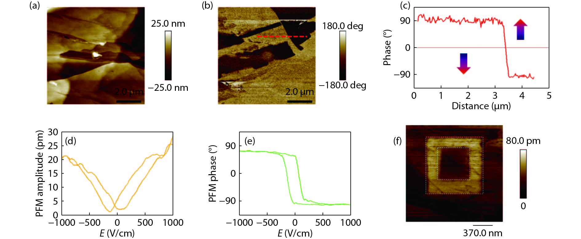
|
| [5] |
Chu M W, Szafraniak I, Scholz R, et al. Impact of misfit dislocations on the polarization instability of epitaxial nanostructured ferroelectric perovskites. Nat Mater, 2004, 3(2), 87 doi: 10.1038/nmat1057 |
| [6] |
Stengel M, Vanderbilt D, Spaldin N A. Enhancement of ferroelectricity at metal–oxide interfaces. Nat Mater, 2009, 8, 392 doi: 10.1038/nmat2429 |
| [7] |
Lu H, Liu X, Burton J D, et al. Enhancement of ferroelectric polarization stability by interface engineering. Adv Mater, 2012, 24(9), 1209 doi: 10.1002/adma.v24.9 |
| [8] |
Junquera J, Ghosez P. Critical thickness for ferroelectricity in perovskite ultrathin films. Nature, 2003, 422(6931), 506 doi: 10.1038/nature01501 |
| [9] |
Gao P, Zhang Z Y, Li M Q, et al. Possible absence of critical thickness and size effect in ultrathin perovskite ferroelectric films. Nat Commun, 2017, 8, 15549 doi: 10.1038/ncomms15549 |
| [10] |
Xi X X, Wang Z F, Zhao W W, et al. Ising pairing in superconducting NbSe 2 atomic layers. Nat Phys, 2015, 12, 139 doi: 10.1038/nphys3538 |
| [11] |
Xi X X, Zhao L, Wang Z F, et al. Strongly enhanced charge-density-wave order in monolayer NbSe 2. Nature Nanotech, 2015, 10, 765 doi: 10.1038/nnano.2015.143 |
| [12] |
Zeng H L, Dai J F, Yao W, et al. Valley polarization in MoS 2 monolayers by optical pumping. Nat Nanotech, 2012, 7, 490 doi: 10.1038/nnano.2012.95 |
| [13] |
Deng Y, Yu Y, Song Y, et al. Gate-tunable room-temperature ferromagnetism in two-dimensional Fe 3GeTe 2. Nature, 2018, 563(7729), 94 doi: 10.1038/s41586-018-0626-9 |
| [14] |
Geim A K, Novoselov K S. The rise of graphene. Nat Mater, 2007, 6, 183 doi: 10.1038/nmat1849 |
| [15] |
Mak K F, Lee C G, Hone J, et al. Atomically thin MoS 2 : a new direct-gap semiconductor. Phys Rev Lett, 2010, 105(13), 136805 doi: 10.1103/PhysRevLett.105.136805 |
| [16] |
Zeng H L, Cui X D. An optical spectroscopic study on two-dimensional group-VI transition metal dichalcogenides. Chem Soc Rev, 2015, 44(9), 2629 doi: 10.1039/C4CS00265B |
| [17] |
Belianinov A, He Q, Dziaugys A, et al. CuInP 2S 6 room temperature layered ferroelectric. Nano Lett, 2015, 15(6), 3808 doi: 10.1021/acs.nanolett.5b00491 |
| [18] |
Liu F C, You L, Seyler K L, et al. Room-temperature ferroelectricity in CuInP 2S 6 ultrathin flakes. Nat Commun, 2016, 7, 12357 doi: 10.1038/ncomms12357 |
| [19] |
Chang K, Liu J W, Lin H C, et al. Discovery of robust in-plane ferroelectricity in atomic-thick SnTe. Science, 2016, 353(6296), 274 doi: 10.1126/science.aad8609 |
| [20] |
Ding W J, Zhu J B, Wang Z, et al. Prediction of intrinsic two-dimensional ferroelectrics in In 2Se 3 and other III 2–VI 3 van der Waals materials. Nat Commun, 2017, 8, 14956 doi: 10.1038/ncomms14956 |
| [21] |
Zhou Y, Wu D, Zhu Y H, et al. Out-of-plane piezoelectricity and ferroelectricity in layered α-In 2Se 3 nanoflakes. Nano Lett, 2017, 17(9), 5508 doi: 10.1021/acs.nanolett.7b02198 |
| [22] |
Cui C J, Hu W J, Yan X X, et al. Intercorrelated in-plane and out-of-plane ferroelectricity in ultrathin two-dimensional layered semiconductor In 2Se 3. Nano Lett, 2018, 18(2), 1253 doi: 10.1021/acs.nanolett.7b04852 |
| [23] |
Poh S M, Tan S J R, Wang H, et al. Molecular-beam epitaxy of two-dimensional In 2Se 3 and its giant electroresistance switching in ferroresistive memory junction. Nano Lett, 2018, 18(10), 6340 doi: 10.1021/acs.nanolett.8b02688 |
| [24] |
Wan S Y, Li Y, Li W, et al. Room-temperature ferroelectricity and a switchable diode effect in two-dimensional α-In 2Se 3 thin layers. Nanoscale, 2018, 10(31), 14885 doi: 10.1039/C8NR04422H |
| [25] |
Xiao J, Zhu H, Wang Y, et al. Intrinsic two-dimensional ferroelectricity with dipole locking. Phys Rev Lett, 2018, 120(22), 227601 doi: 10.1103/PhysRevLett.120.227601 |
| [26] |
Xue F, Hu W, Lee K C, et al. Room-temperature ferroelectricity in hexagonally layered α-In 2Se 3 nanoflakes down to the monolayer limit. Adv Funct Mater, 2018, 0(0), 1803738 doi: 10.1002/adfm.201803738 |
| [27] |
Xue F, Zhang J, Hu W, et al. Multidirection piezoelectricity in mono- and multilayered hexagonal α-In 2Se 3. ACS Nano, 2018, 12(5), 4976 doi: 10.1021/acsnano.8b02152 |
| [28] |
Zheng C, Yu L, Zhu L, et al. Room temperature in-plane ferroelectricity in van der Waals In 2Se 3. Sci Adv, 2018, 4(7), eaar7720 doi: 10.1126/sciadv.aar7720 |
| [29] |
Wan S Y, Li Y, Li W, et al. Nonvolatile ferroelectric memory effect in ultrathin α-In 2Se 3. Adv Funct Mater, 2018, 29, 1808606 doi: 10.1002/adfm.201808606 |
| [30] |
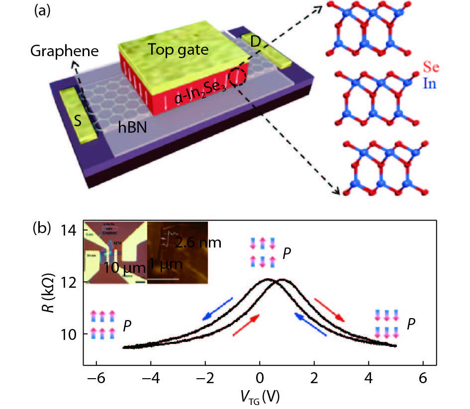
Si M W, Gao S J, Qiu G, et all. A ferroelectric semiconductor field-effect transistor. arXiv: 1812.02933
|
| [31] |
Tao X, Gu Y. Crystalline–crystalline phase transformation in two-dimensional In 2Se 3 thin layers. Nano Lett, 2013, 13(8), 3501 doi: 10.1021/nl400888p |
| [32] |
Wu D, Pak A J, Liu Y N, et al. Thickness-dependent dielectric constant of few-layer In 2Se 3 nanoflakes. Nano Lett, 2015, 15(12), 8136 doi: 10.1021/acs.nanolett.5b03575 |
| [33] |
Zhou J D, Zeng Q S, Lv D H, et al. Controlled synthesis of high-quality monolayered α-In 2Se 3 via physical vapor deposition. Nano Lett, 2015, 15(10), 6400 doi: 10.1021/acs.nanolett.5b01590 |
| [34] |
Jacobs-Gedrim R B, Shanmugam M, Jain N, et al. Extraordinary photoresponse in two-dimensional In 2Se 3 nanosheets. ACS Nano, 2014, 8(1), 514 doi: 10.1021/nn405037s |
| [35] |
Nilanthy B, Christopher R S, Emily F S, et al. Quantum confinement and photoresponsivity of β -In 2Se 3 nanosheets grown by physical vapour transport. 2D Mater, 2016, 3(2), 025030 doi: 10.1088/2053-1583/3/2/025030 |
| [36] |
Choi M S, Cheong B K, Ra C H, et al. Electrically driven reversible phase changes in layered In 2Se 3 crystalline film. Adv Mater, 2017, 29(42), 1703568 doi: 10.1002/adma.201703568 |
| [37] |
Lewandowska R, Bacewicz R, Filipowicz J, et al. Raman scattering in α-In 2Se 3 crystals. Mater Res Bull, 2001, 36(15), 2577 doi: 10.1016/S0025-5408(01)00746-2 |
| [38] |
Debbichi L, Eriksson O, Lebègue S. Two-dimensional indium selenides compounds: an ab initio study. J Phys Chem Lett, 2015, 6(15), 3098 doi: 10.1021/acs.jpclett.5b01356 |
| [39] |
Zhou S, Tao X, Gu Y. Thickness-dependent thermal conductivity of suspended two-dimensional single-crystal In 2Se 3 layers grown by chemical vapor deposition. J Phys Chem C, 2016, 120(9), 4753 doi: 10.1021/acs.jpcc.5b10905 |
| [40] |
Eisuke T, Kojiro O, Hiroshi I. Low voltage operation of nonvolatile metal–ferroelectric–metal–insulator–semiconductor (MFMIS) field-effect-transistors (FETs) using Pt/SrBi 2Ta 2O 9/Pt/SrTa 2O 6/SiON/Si structures. Jpn J Appl Phys, 2001, 40(4S), 2917 doi: 10.1143/JJAP.40.2917 |
| [41] |
Eisuke T, Gen F, Hiroshi I. Electrical properties of metal–ferroelectric–insulator–semiconductor (MFIS) and metal–ferroelectric–metal–insulator–semiconductor (MFMIS)-FETs using ferroelectric SrBi 2Ta 2O 9 film and SrTa 2O 6/SiON buffer layer. Jpn J Appl Phys, 2000, 39(4S), 2125 doi: 10.1143/JJAP.39.2125 |


 DownLoad: