


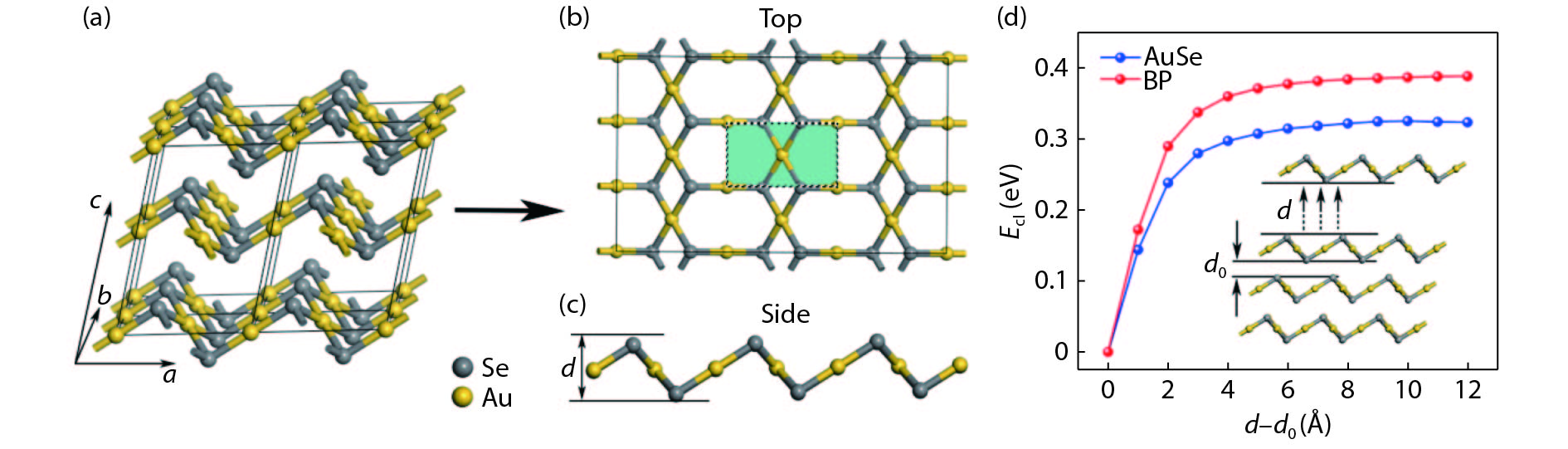
Fig. 1.
(Color online) Structure of (a) bulk AuSe with 2 × 2 × 1 supercell, (b) two dimensional AuSe in top view and (c) side view. (d) Cleavage energy of AuSe monolayer and black phorphous.
ARTICLES
Pengxiang Bai, Shiying Guo, Shengli Zhang, Hengze Qu, Wenhan Zhou and Haibo Zeng
Corresponding author: Shengli Zhang, E-mail addresses: zhangslvip@njust.edu.cn; zeng.haibo@njust.edu.cn; Haibo Zeng, E-mail addresses: zhangslvip@njust.edu.cn; zeng.haibo@njust.edu.cn
Abstract: As a large family of 2D materials, transition metal dichalcogenides (TMDs) have stimulated numerous works owing to their attractive properties. The replacement of constituent elements could promote the discovery and fabrication of new nano-film in this family. Using precious metals, such as platinum and palladium, to serve as transition metals combined with chalcogen is a new approach to explore novel TMDs. Also, the proportion between transition metal and chalcogen atoms is found not only to exist in conventional form of 1 : 2. Herein, we reported a comprehensive study of a new 2D precious metal selenide, namely AuSe monolayer. Based on density functional theory, our result indicated that AuSe monolayer is a semiconductor with indirect band-gap of 2.0 eV, which possesses superior dynamic stability and thermodynamic stability with cohesive energy up to –7.87 eV/atom. Moreover, it has been confirmed that ionic bonding predominates in Au–Se bonds and absorption peaks in all directions distribute in the deep ultraviolet region. In addition, both vibration modes dominating marked Raman peaks are parallel to the 2D plane.
Keywords: AuSe monolayer, DFT calculation, 2D semiconductor
| [1] |
Novoselov K S, Geim A K, Morozov S V, et al. Electric field effect in atomically thin carbon films. Science, 2004, 306, 666 doi: 10.1126/science.1102896
|
| [2] |
Mak K F, Lee C, Hone J, et al. Atomically thin MoS2: a new direct-gap semiconductor. Phys Rev Lett, 2010, 105, 136805 doi: 10.1103/PhysRevLett.105.136805
|
| [3] |
Radisavljevic B, Radenovic A, Brivio J, et al. Single-layer MoS2 transistors. Nat Nanotechnol, 2011, 6, 147 doi: 10.1038/nnano.2010.279
|
| [4] |
Wang Q H, Kalantar-Zadeh K, Kis A, et al. Electronics and optoelectronics of two-dimensional transition metal dichalcogenides. Nat Nanotechnol, 2012, 7, 699 doi: 10.1038/nnano.2012.193
|
| [5] |
Zhang Y, Ye J, Matsuhashi Y, et al. Ambipolar MoS2 thin flake transistors. Nano Lett, 2012, 12, 1136 doi: 10.1021/nl2021575
|
| [6] |
Mak K F, Shan J. Photonics and optoelectronics of 2D semiconductor transition metal dichalcogenides. Nat Photon, 2016, 10, 216 doi: 10.1038/nphoton.2015.282
|
| [7] |
Tan C, Zhang H. Two-dimensional transition metal dichalcogenide nanosheet-based composites. Chem Soc Rev, 2015, 44, 2713 doi: 10.1039/C4CS00182F
|
| [8] |
Yun W S, Han S W, Hong S C, et al. Thickness and strain effects on electronic structures of transition metal dichalcogenides: 2H-MX2 semiconductors (M = Mo, W; X = S, Se, Te). Phys Rev B, 2012, 85, 033305 doi: 10.1103/PhysRevB.85.033305
|
| [9] |
Sajjad M, Singh N, Schwingenschlögl U. Strongly bound excitons in monolayer PtS2 and PtSe2. Appl Phys Lett, 2018, 112, 043101 doi: 10.1063/1.5010881
|
| [10] |
Wang Y, Li L, Yao W, et al. Monolayer PtSe2, a new semiconducting transition-metal-dichalcogenide, epitaxially grown by direct selenization of Pt. Nano Lett, 2015, 15, 4013 doi: 10.1021/acs.nanolett.5b00964
|
| [11] |
Yim C, Lee K, McEvoy N, et al. High-performance hybrid electronic devices from layered PtSe2 films grown at low temperature. ACS Nano, 2016, 10, 9550 doi: 10.1021/acsnano.6b04898
|
| [12] |
Zhang K, Yan M, Zhang H, et al. Experimental evidence for type-II Dirac semimetal in PtSe2. Phys Rev B, 2017, 96, 125102 doi: 10.1103/PhysRevB.96.125102
|
| [13] |
Sun J F, Shi H L, Siegrist T, et al. Electronic, transport, and optical properties of bulk and mono-layer PdSe2. Appl Phys Lett, 2015, 107, 153902 doi: 10.1063/1.4933302
|
| [14] |
Wang Y, Li Y, Chen Z. Not your familiar two dimensional transition metal disulfide: structural and electronic properties of the PdS2 monolayer. J Mater Chem C, 2015, 3, 9603 doi: 10.1039/C5TC01345C
|
| [15] |
Wu Q, Xu W W, Qu B, et al. Au6S2 monolayer sheets: metallic and semiconducting polymorphs. Mater Horiz, 2017, 4, 1085 doi: 10.1039/C7MH00461C
|
| [16] |
Peng R, Ma Y, He Z, et al. Single-layer Ag2S: A two-dimensional bi-directional auxetic semiconductor. Nano Lett, 2019, 19(2), 1227 doi: 10.1021/acs.nanolett.8b04761
|
| [17] |
Machogo L F E, Tetyana P, Sithole R, et al. Unravelling the structural properties of mixed-valence α- and β-AuSe nanostructures using XRD, TEM and XPS. Appl Surf Sci, 2018, 456, 973 doi: 10.1016/j.apsusc.2018.06.141
|
| [18] |
Clark S J, Segall M D, Pickard C J, et al. First principles methods using CASTEP. Z Kristallogr, 2005, 220, 567
|
| [19] |
Kresse G, Furthümller J. Efficient iterative schemes for ab initio total-energy calculations using a plane-wave basis set. Phys Rev B, 1996, 54, 11169 doi: 10.1103/PhysRevB.54.11169
|
| [20] |
Perdew J P, Burke K, Ernzerhof M. Generalized gradient approximation made simple. Phys Rev Lett, 1996, 77, 3865 doi: 10.1103/PhysRevLett.77.3865
|
| [21] |
Heyd J, Scuseria G E, Ernzerhof M. Hybrid functionals based on a screened Coulomb potential. J Chem Phys, 2003, 118, 8207 doi: 10.1063/1.1564060
|
| [22] |
Paier J, Marsman M, Hummer K, et al. Screened hybrid density functionals applied to solids. J Chem Phys, 2006, 124, 154709 doi: 10.1063/1.2187006
|
| [23] |
Liu H, Neal A T, Zhu Z, et al. Phosphorene: An unexplored 2D semiconductor with a high hole mobility. ACS Nano, 2014, 8, 4033 doi: 10.1021/nn501226z
|
| [24] |
Li L, Yu Y, Ye G J, et al. Black phosphorus field-effect transistors. Nat Nanotechnol, 2014, 9, 372 doi: 10.1038/nnano.2014.35
|
| [25] |
Qiao J, Kong X, Hu Z X, et al. High-mobility transport anisotropy and linear dichroism in few-layer black phosphorus. Nat Commun, 2014, 5, 4475 doi: 10.1038/ncomms5475
|
| [26] |
Zhang S, Guo S, Chen Z, et al. Recent progress in 2D group-VA semiconductors: from theory to experiment. Chem Soc Rev, 2018, 47, 982 doi: 10.1039/C7CS00125H
|
| [27] |
Zhang S, Xie M, Li F, et al. Semiconducting group 15 monolayers: a broad range of band gaps and high carrier mobilities. Angew Chem Int Ed Engl, 2016, 55, 1666 doi: 10.1002/anie.201507568
|
| [28] |
Zhang S, Yan Z, Li Y, et al. Atomically thin arsenene and antimonene: semimetal–semiconductor and indirect-direct band-gap transitions. Angew Chem Int Ed Engl, 2015, 54, 3112 doi: 10.1002/anie.201411246
|
| [29] |
Koskinen P, Malola S, Hakkinen H. Self-passivating edge reconstructions of graphene. Phys Rev Lett, 2008, 101, 115502 doi: 10.1103/PhysRevLett.101.115502
|
| [30] |
Şahin H, Cahangirov S, Topsakal M, et al. Monolayer honeycomb structures of group-IV elements and III–V binary compounds: First-principles calculations. Phys Rev B, 2009, 80, 155453 doi: 10.1103/PhysRevB.80.155453
|
| [31] |
Topsakal M, Aktürk E, Ciraci S. First-principles study of two- and one-dimensional honeycomb structures of boron nitride. Phys Rev B, 2009, 79, 115442 doi: 10.1103/PhysRevB.79.115442
|
| [32] |
Silvi B, Savin A. Classification of chemical bonds based on topological analysis of electron localization functions. Nature, 1994, 317, 683 doi: 10.1038/371683a0
|
| [33] |
Li J, Fan Z Y, Dahal R, et al. 200 nm deep ultraviolet photodetectors based on AlN. Appl Phys Lett, 2006, 89, 213510 doi: 10.1063/1.2397021
|
| [34] |
Sajjad M, Jadwisienczak W M, Feng P. Nanoscale structure study of boron nitride nanosheets and development of a deep-UV photo-detector. Nanoscale, 2014, 6, 4577 doi: 10.1039/C3NR05817D
|
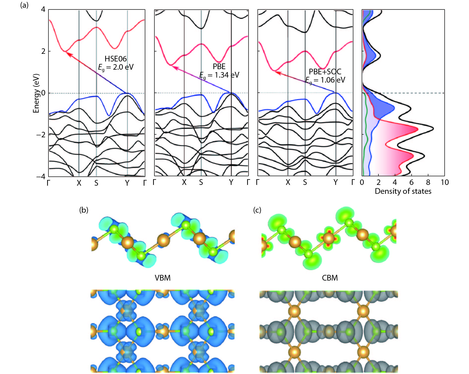
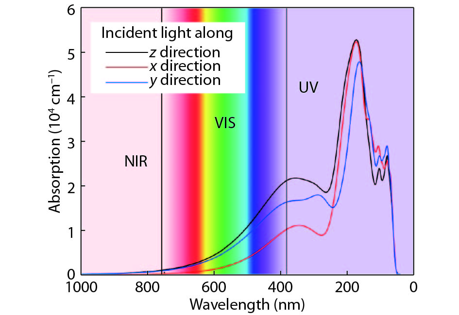
Table 1. Optimized lattice parameters of AuSe monolayer.
| Material | Bond length (Å) | Bond angle (deg) | Lattice parameters (deg) | ||||||
| d1 | d2 | θ1 | θ2 | θ3 | α | γ | |||
| AuSe | 2.49 | 2.41 | 94.73 | 85.27 | 97.45 | 90.00 | 84.13 | ||
 DownLoad: CSV
| [1] |
Novoselov K S, Geim A K, Morozov S V, et al. Electric field effect in atomically thin carbon films. Science, 2004, 306, 666 doi: 10.1126/science.1102896
|
| [2] |
Mak K F, Lee C, Hone J, et al. Atomically thin MoS2: a new direct-gap semiconductor. Phys Rev Lett, 2010, 105, 136805 doi: 10.1103/PhysRevLett.105.136805
|
| [3] |
Radisavljevic B, Radenovic A, Brivio J, et al. Single-layer MoS2 transistors. Nat Nanotechnol, 2011, 6, 147 doi: 10.1038/nnano.2010.279
|
| [4] |
Wang Q H, Kalantar-Zadeh K, Kis A, et al. Electronics and optoelectronics of two-dimensional transition metal dichalcogenides. Nat Nanotechnol, 2012, 7, 699 doi: 10.1038/nnano.2012.193
|
| [5] |
Zhang Y, Ye J, Matsuhashi Y, et al. Ambipolar MoS2 thin flake transistors. Nano Lett, 2012, 12, 1136 doi: 10.1021/nl2021575
|
| [6] |
Mak K F, Shan J. Photonics and optoelectronics of 2D semiconductor transition metal dichalcogenides. Nat Photon, 2016, 10, 216 doi: 10.1038/nphoton.2015.282
|
| [7] |
Tan C, Zhang H. Two-dimensional transition metal dichalcogenide nanosheet-based composites. Chem Soc Rev, 2015, 44, 2713 doi: 10.1039/C4CS00182F
|
| [8] |
Yun W S, Han S W, Hong S C, et al. Thickness and strain effects on electronic structures of transition metal dichalcogenides: 2H-MX2 semiconductors (M = Mo, W; X = S, Se, Te). Phys Rev B, 2012, 85, 033305 doi: 10.1103/PhysRevB.85.033305
|
| [9] |
Sajjad M, Singh N, Schwingenschlögl U. Strongly bound excitons in monolayer PtS2 and PtSe2. Appl Phys Lett, 2018, 112, 043101 doi: 10.1063/1.5010881
|
| [10] |
Wang Y, Li L, Yao W, et al. Monolayer PtSe2, a new semiconducting transition-metal-dichalcogenide, epitaxially grown by direct selenization of Pt. Nano Lett, 2015, 15, 4013 doi: 10.1021/acs.nanolett.5b00964
|
| [11] |
Yim C, Lee K, McEvoy N, et al. High-performance hybrid electronic devices from layered PtSe2 films grown at low temperature. ACS Nano, 2016, 10, 9550 doi: 10.1021/acsnano.6b04898
|
| [12] |
Zhang K, Yan M, Zhang H, et al. Experimental evidence for type-II Dirac semimetal in PtSe2. Phys Rev B, 2017, 96, 125102 doi: 10.1103/PhysRevB.96.125102
|
| [13] |
Sun J F, Shi H L, Siegrist T, et al. Electronic, transport, and optical properties of bulk and mono-layer PdSe2. Appl Phys Lett, 2015, 107, 153902 doi: 10.1063/1.4933302
|
| [14] |
Wang Y, Li Y, Chen Z. Not your familiar two dimensional transition metal disulfide: structural and electronic properties of the PdS2 monolayer. J Mater Chem C, 2015, 3, 9603 doi: 10.1039/C5TC01345C
|
| [15] |
Wu Q, Xu W W, Qu B, et al. Au6S2 monolayer sheets: metallic and semiconducting polymorphs. Mater Horiz, 2017, 4, 1085 doi: 10.1039/C7MH00461C
|
| [16] |
Peng R, Ma Y, He Z, et al. Single-layer Ag2S: A two-dimensional bi-directional auxetic semiconductor. Nano Lett, 2019, 19(2), 1227 doi: 10.1021/acs.nanolett.8b04761
|
| [17] |
Machogo L F E, Tetyana P, Sithole R, et al. Unravelling the structural properties of mixed-valence α- and β-AuSe nanostructures using XRD, TEM and XPS. Appl Surf Sci, 2018, 456, 973 doi: 10.1016/j.apsusc.2018.06.141
|
| [18] |
Clark S J, Segall M D, Pickard C J, et al. First principles methods using CASTEP. Z Kristallogr, 2005, 220, 567
|
| [19] |
Kresse G, Furthümller J. Efficient iterative schemes for ab initio total-energy calculations using a plane-wave basis set. Phys Rev B, 1996, 54, 11169 doi: 10.1103/PhysRevB.54.11169
|
| [20] |
Perdew J P, Burke K, Ernzerhof M. Generalized gradient approximation made simple. Phys Rev Lett, 1996, 77, 3865 doi: 10.1103/PhysRevLett.77.3865
|
| [21] |
Heyd J, Scuseria G E, Ernzerhof M. Hybrid functionals based on a screened Coulomb potential. J Chem Phys, 2003, 118, 8207 doi: 10.1063/1.1564060
|
| [22] |
Paier J, Marsman M, Hummer K, et al. Screened hybrid density functionals applied to solids. J Chem Phys, 2006, 124, 154709 doi: 10.1063/1.2187006
|
| [23] |
Liu H, Neal A T, Zhu Z, et al. Phosphorene: An unexplored 2D semiconductor with a high hole mobility. ACS Nano, 2014, 8, 4033 doi: 10.1021/nn501226z
|
| [24] |
Li L, Yu Y, Ye G J, et al. Black phosphorus field-effect transistors. Nat Nanotechnol, 2014, 9, 372 doi: 10.1038/nnano.2014.35
|
| [25] |
Qiao J, Kong X, Hu Z X, et al. High-mobility transport anisotropy and linear dichroism in few-layer black phosphorus. Nat Commun, 2014, 5, 4475 doi: 10.1038/ncomms5475
|
| [26] |
Zhang S, Guo S, Chen Z, et al. Recent progress in 2D group-VA semiconductors: from theory to experiment. Chem Soc Rev, 2018, 47, 982 doi: 10.1039/C7CS00125H
|
| [27] |
Zhang S, Xie M, Li F, et al. Semiconducting group 15 monolayers: a broad range of band gaps and high carrier mobilities. Angew Chem Int Ed Engl, 2016, 55, 1666 doi: 10.1002/anie.201507568
|
| [28] |
Zhang S, Yan Z, Li Y, et al. Atomically thin arsenene and antimonene: semimetal–semiconductor and indirect-direct band-gap transitions. Angew Chem Int Ed Engl, 2015, 54, 3112 doi: 10.1002/anie.201411246
|
| [29] |
Koskinen P, Malola S, Hakkinen H. Self-passivating edge reconstructions of graphene. Phys Rev Lett, 2008, 101, 115502 doi: 10.1103/PhysRevLett.101.115502
|
| [30] |
Şahin H, Cahangirov S, Topsakal M, et al. Monolayer honeycomb structures of group-IV elements and III–V binary compounds: First-principles calculations. Phys Rev B, 2009, 80, 155453 doi: 10.1103/PhysRevB.80.155453
|
| [31] |
Topsakal M, Aktürk E, Ciraci S. First-principles study of two- and one-dimensional honeycomb structures of boron nitride. Phys Rev B, 2009, 79, 115442 doi: 10.1103/PhysRevB.79.115442
|
| [32] |
Silvi B, Savin A. Classification of chemical bonds based on topological analysis of electron localization functions. Nature, 1994, 317, 683 doi: 10.1038/371683a0
|
| [33] |
Li J, Fan Z Y, Dahal R, et al. 200 nm deep ultraviolet photodetectors based on AlN. Appl Phys Lett, 2006, 89, 213510 doi: 10.1063/1.2397021
|
| [34] |
Sajjad M, Jadwisienczak W M, Feng P. Nanoscale structure study of boron nitride nanosheets and development of a deep-UV photo-detector. Nanoscale, 2014, 6, 4577 doi: 10.1039/C3NR05817D
|


Article views: 5616 Times PDF downloads: 148 Times Cited by: 0 Times
Received: 26 March 2019 Revised: 05 May 2019 Online: Accepted Manuscript: 16 May 2019Uncorrected proof: 23 May 2019Published: 05 June 2019
| Citation: |
Pengxiang Bai, Shiying Guo, Shengli Zhang, Hengze Qu, Wenhan Zhou, Haibo Zeng. Electronic band structures and optical properties of atomically thin AuSe: first-principle calculations[J]. Journal of Semiconductors, 2019, 40(6): 062004. doi: 10.1088/1674-4926/40/6/062004
****
P X Bai, S Y Guo, S L Zhang, H Z Qu, W H Zhou, H B Zeng, Electronic band structures and optical properties of atomically thin AuSe: first-principle calculations[J]. J. Semicond., 2019, 40(6): 062004. doi: 10.1088/1674-4926/40/6/062004.

|
| [1] |
Novoselov K S, Geim A K, Morozov S V, et al. Electric field effect in atomically thin carbon films. Science, 2004, 306, 666 doi: 10.1126/science.1102896
|
| [2] |
Mak K F, Lee C, Hone J, et al. Atomically thin MoS2: a new direct-gap semiconductor. Phys Rev Lett, 2010, 105, 136805 doi: 10.1103/PhysRevLett.105.136805
|
| [3] |
Radisavljevic B, Radenovic A, Brivio J, et al. Single-layer MoS2 transistors. Nat Nanotechnol, 2011, 6, 147 doi: 10.1038/nnano.2010.279
|
| [4] |
Wang Q H, Kalantar-Zadeh K, Kis A, et al. Electronics and optoelectronics of two-dimensional transition metal dichalcogenides. Nat Nanotechnol, 2012, 7, 699 doi: 10.1038/nnano.2012.193
|
| [5] |
Zhang Y, Ye J, Matsuhashi Y, et al. Ambipolar MoS2 thin flake transistors. Nano Lett, 2012, 12, 1136 doi: 10.1021/nl2021575
|
| [6] |
Mak K F, Shan J. Photonics and optoelectronics of 2D semiconductor transition metal dichalcogenides. Nat Photon, 2016, 10, 216 doi: 10.1038/nphoton.2015.282
|
| [7] |
Tan C, Zhang H. Two-dimensional transition metal dichalcogenide nanosheet-based composites. Chem Soc Rev, 2015, 44, 2713 doi: 10.1039/C4CS00182F
|
| [8] |
Yun W S, Han S W, Hong S C, et al. Thickness and strain effects on electronic structures of transition metal dichalcogenides: 2H-MX2 semiconductors (M = Mo, W; X = S, Se, Te). Phys Rev B, 2012, 85, 033305 doi: 10.1103/PhysRevB.85.033305
|
| [9] |
Sajjad M, Singh N, Schwingenschlögl U. Strongly bound excitons in monolayer PtS2 and PtSe2. Appl Phys Lett, 2018, 112, 043101 doi: 10.1063/1.5010881
|
| [10] |
Wang Y, Li L, Yao W, et al. Monolayer PtSe2, a new semiconducting transition-metal-dichalcogenide, epitaxially grown by direct selenization of Pt. Nano Lett, 2015, 15, 4013 doi: 10.1021/acs.nanolett.5b00964
|
| [11] |
Yim C, Lee K, McEvoy N, et al. High-performance hybrid electronic devices from layered PtSe2 films grown at low temperature. ACS Nano, 2016, 10, 9550 doi: 10.1021/acsnano.6b04898
|
| [12] |
Zhang K, Yan M, Zhang H, et al. Experimental evidence for type-II Dirac semimetal in PtSe2. Phys Rev B, 2017, 96, 125102 doi: 10.1103/PhysRevB.96.125102
|
| [13] |
Sun J F, Shi H L, Siegrist T, et al. Electronic, transport, and optical properties of bulk and mono-layer PdSe2. Appl Phys Lett, 2015, 107, 153902 doi: 10.1063/1.4933302
|
| [14] |
Wang Y, Li Y, Chen Z. Not your familiar two dimensional transition metal disulfide: structural and electronic properties of the PdS2 monolayer. J Mater Chem C, 2015, 3, 9603 doi: 10.1039/C5TC01345C
|
| [15] |
Wu Q, Xu W W, Qu B, et al. Au6S2 monolayer sheets: metallic and semiconducting polymorphs. Mater Horiz, 2017, 4, 1085 doi: 10.1039/C7MH00461C
|
| [16] |
Peng R, Ma Y, He Z, et al. Single-layer Ag2S: A two-dimensional bi-directional auxetic semiconductor. Nano Lett, 2019, 19(2), 1227 doi: 10.1021/acs.nanolett.8b04761
|
| [17] |
Machogo L F E, Tetyana P, Sithole R, et al. Unravelling the structural properties of mixed-valence α- and β-AuSe nanostructures using XRD, TEM and XPS. Appl Surf Sci, 2018, 456, 973 doi: 10.1016/j.apsusc.2018.06.141
|
| [18] |
Clark S J, Segall M D, Pickard C J, et al. First principles methods using CASTEP. Z Kristallogr, 2005, 220, 567
|
| [19] |
Kresse G, Furthümller J. Efficient iterative schemes for ab initio total-energy calculations using a plane-wave basis set. Phys Rev B, 1996, 54, 11169 doi: 10.1103/PhysRevB.54.11169
|
| [20] |
Perdew J P, Burke K, Ernzerhof M. Generalized gradient approximation made simple. Phys Rev Lett, 1996, 77, 3865 doi: 10.1103/PhysRevLett.77.3865
|
| [21] |
Heyd J, Scuseria G E, Ernzerhof M. Hybrid functionals based on a screened Coulomb potential. J Chem Phys, 2003, 118, 8207 doi: 10.1063/1.1564060
|
| [22] |
Paier J, Marsman M, Hummer K, et al. Screened hybrid density functionals applied to solids. J Chem Phys, 2006, 124, 154709 doi: 10.1063/1.2187006
|
| [23] |
Liu H, Neal A T, Zhu Z, et al. Phosphorene: An unexplored 2D semiconductor with a high hole mobility. ACS Nano, 2014, 8, 4033 doi: 10.1021/nn501226z
|
| [24] |
Li L, Yu Y, Ye G J, et al. Black phosphorus field-effect transistors. Nat Nanotechnol, 2014, 9, 372 doi: 10.1038/nnano.2014.35
|
| [25] |
Qiao J, Kong X, Hu Z X, et al. High-mobility transport anisotropy and linear dichroism in few-layer black phosphorus. Nat Commun, 2014, 5, 4475 doi: 10.1038/ncomms5475
|
| [26] |
Zhang S, Guo S, Chen Z, et al. Recent progress in 2D group-VA semiconductors: from theory to experiment. Chem Soc Rev, 2018, 47, 982 doi: 10.1039/C7CS00125H
|
| [27] |
Zhang S, Xie M, Li F, et al. Semiconducting group 15 monolayers: a broad range of band gaps and high carrier mobilities. Angew Chem Int Ed Engl, 2016, 55, 1666 doi: 10.1002/anie.201507568
|
| [28] |
Zhang S, Yan Z, Li Y, et al. Atomically thin arsenene and antimonene: semimetal–semiconductor and indirect-direct band-gap transitions. Angew Chem Int Ed Engl, 2015, 54, 3112 doi: 10.1002/anie.201411246
|
| [29] |
Koskinen P, Malola S, Hakkinen H. Self-passivating edge reconstructions of graphene. Phys Rev Lett, 2008, 101, 115502 doi: 10.1103/PhysRevLett.101.115502
|
| [30] |
Şahin H, Cahangirov S, Topsakal M, et al. Monolayer honeycomb structures of group-IV elements and III–V binary compounds: First-principles calculations. Phys Rev B, 2009, 80, 155453 doi: 10.1103/PhysRevB.80.155453
|
| [31] |
Topsakal M, Aktürk E, Ciraci S. First-principles study of two- and one-dimensional honeycomb structures of boron nitride. Phys Rev B, 2009, 79, 115442 doi: 10.1103/PhysRevB.79.115442
|
| [32] |
Silvi B, Savin A. Classification of chemical bonds based on topological analysis of electron localization functions. Nature, 1994, 317, 683 doi: 10.1038/371683a0
|
| [33] |
Li J, Fan Z Y, Dahal R, et al. 200 nm deep ultraviolet photodetectors based on AlN. Appl Phys Lett, 2006, 89, 213510 doi: 10.1063/1.2397021
|
| [34] |
Sajjad M, Jadwisienczak W M, Feng P. Nanoscale structure study of boron nitride nanosheets and development of a deep-UV photo-detector. Nanoscale, 2014, 6, 4577 doi: 10.1039/C3NR05817D
|

 WeChat ID
Journal of Semiconductors © 2017 All Rights Reserved 京ICP备05085259号-2


