


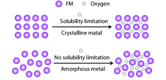
Fig. 1.
(Color online) Schematic diagram for including oxygen in crystalline and amorphous metals. FM denotes ferromagnetic metals.
REVIEWS
Na Chen1, , Kaixuan Fang1, Hongxia Zhang1, Yingqi Zhang1, Wenjian Liu1, Kefu Yao1 and Zhengjun Zhang2
Corresponding author: Na Chen, chennadm@mail.tsinghua.edu.cn
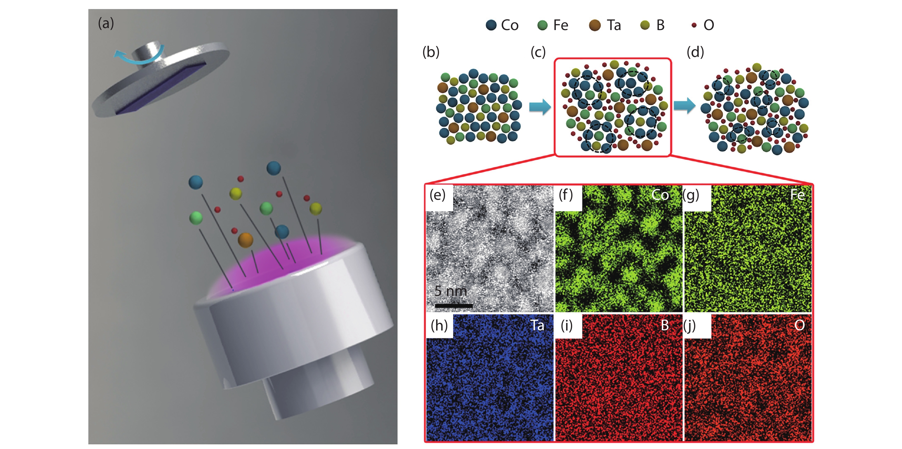
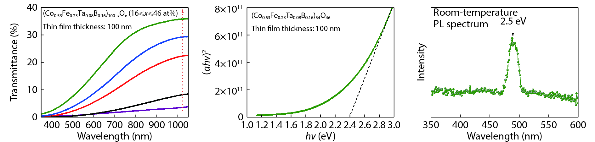
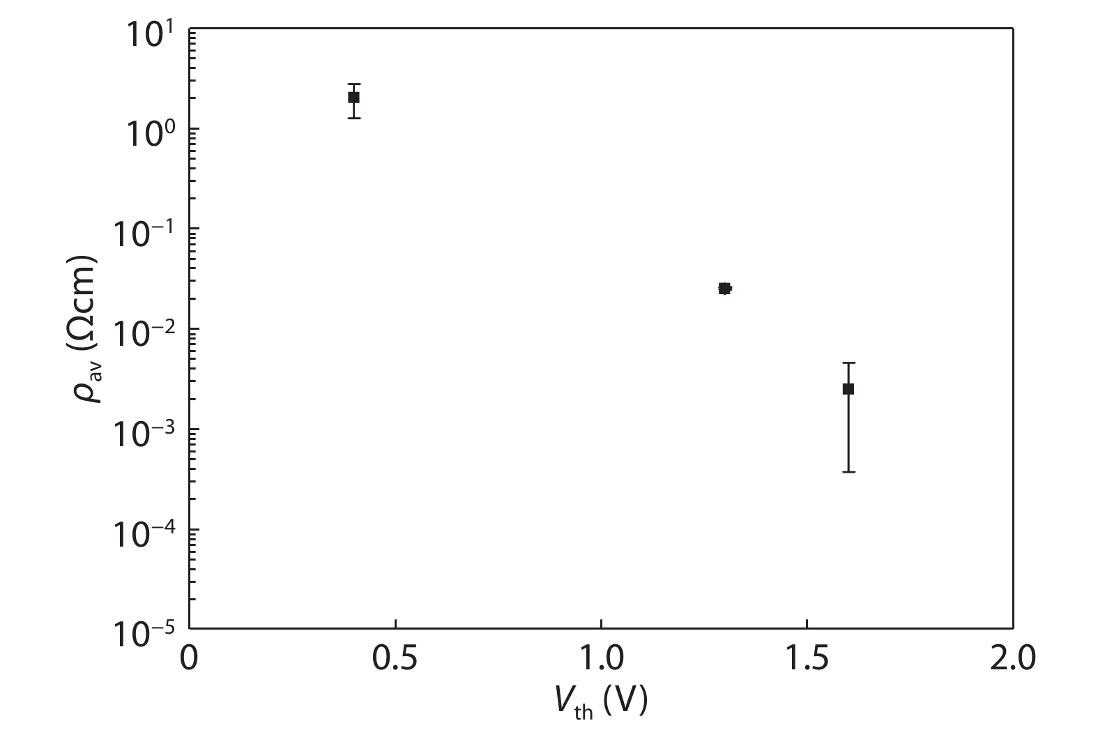
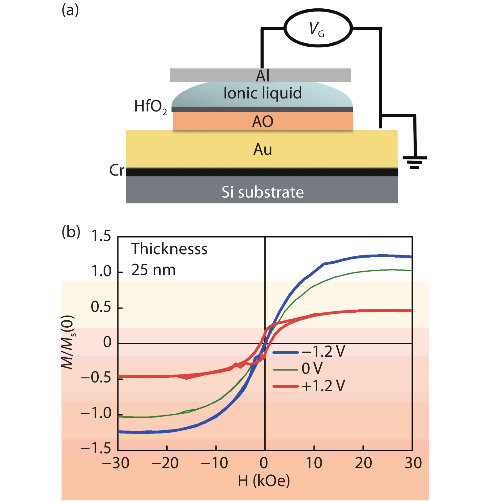
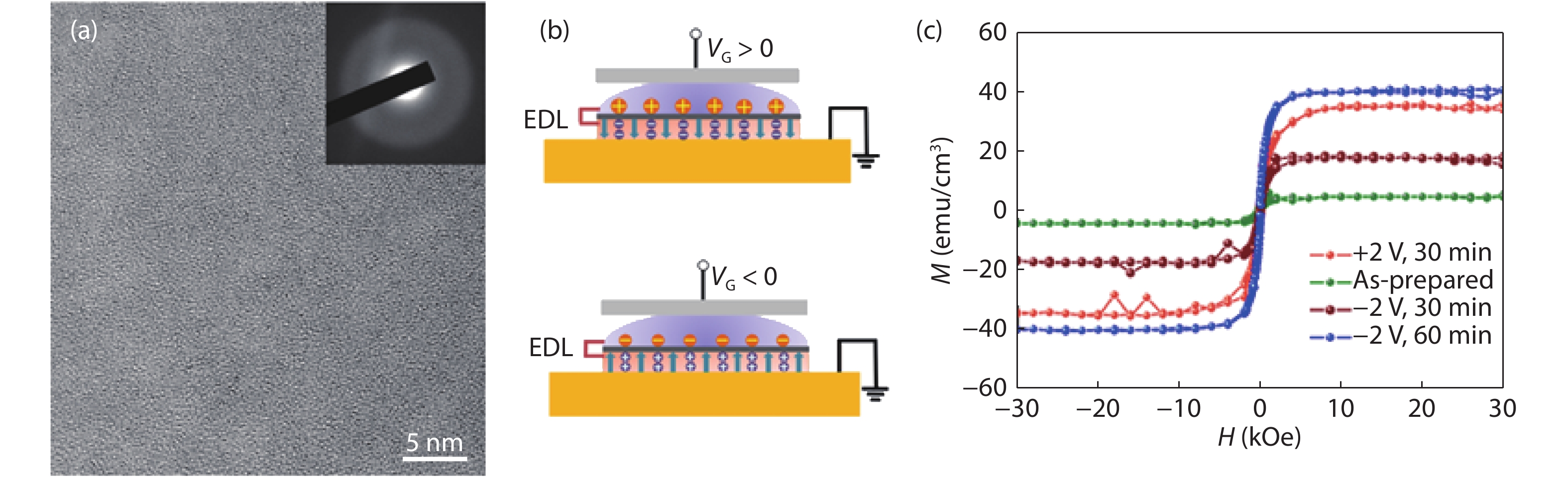
Abstract: Recently, amorphous magnetic semiconductors as a new family of magnetic semiconductors have been developed by oxidizing ferromagnetic amorphous metals/alloys. Intriguingly, tuning the relative atomic ratios of Co and Fe in a Co-Fe-Ta-B-O system leads to the formation of an intrinsic magnetic semiconductor. Starting from high Curie-temperature amorphous ferromagnets, these amorphous magnetic semiconductors show Curie temperatures well above room temperature. Among them, one typical example is a p-type Co28.6Fe12.4Ta4.3B8.7O46 magnetic semiconductor, which has an optical bandgap of ~2.4 eV, room-temperature saturation magnetization of ~433 emu/cm3, and the Curie temperature above 600 K. The amorphous Co28.6Fe12.4Ta4.3B8.7O46 magnetic semiconductor can be integrated with n-type Si to form p–n heterojunctions with a threshold voltage of ~1.6 V, validating its p-type semiconducting character. Furthermore, the demonstration of electric field control of its room-temperature ferromagnetism reflects the interplay between the electricity and ferromagnetism in this material. It is suggested that the carrier density, ferromagnetism and conduction type of an intrinsic magnetic semiconductor are controllable by means of an electric field effect. These findings may pave a new way to realize magnetic semiconductor-based spintronic devices that work at room temperature.
Keywords: CoFeTaBO, amorphous magnetic semiconductors, electric field control of ferromagnetism, metal–semiconductor transition
| [1] |
Holtzberg F, McGuire T R, Methfessel S, et al. Effect of electron concentration on magnetic exchange interactions in rare earth chalcogenides. Phys Rev Lett, 1964, 13, 18 doi: 10.1103/PhysRevLett.13.18
|
| [2] |
Kasuya T, Yanase A. Anomalous transport phenomena in Eu-chalcogenide alloys. Rev Mod Phys, 1968, 40, 684 doi: 10.1103/RevModPhys.40.684
|
| [3] |
Methfessel S. Potential applications of magnetic rare earth compounds. IEEE Trans Mag, 1965, 1, 144 doi: 10.1109/TMAG.1965.1062951
|
| [4] |
Furdyna J K, Kossut J. Diluted magnetic semicondcutors. Vol. 25. In: Semiconductor and semimetals. New York: Academic Press, 1988
|
| [5] |
Dietl T, Ohno H. Dilute ferromagnetic semiconductors: physics and spintronic structures. Rev Mod Phys, 2014, 86, 187 doi: 10.1103/RevModPhys.86.187
|
| [6] |
Ohno H. Making nonmagnetic semiconductors ferromagnetic. Science, 1998, 281, 951 doi: 10.1126/science.281.5379.951
|
| [7] |
Ohno H, Shen A, Matsukura F, et al. (Ga,Mn)As: A new diluted magnetic semiconductor based on GaAs. Appl Phys Lett, 1996, 69, 363 doi: 10.1063/1.118061
|
| [8] |
Munekata H, Ohno H, von Molnár S, et al. Diluted magnetic III–V semiconductors. Phys Rev Lett, 1989, 63, 1849 doi: 10.1103/PhysRevLett.63.1849
|
| [9] |
Chen L, Yang X, Yang F H, et al. Enhancing the Curie temperature of ferromagnetic semiconductor (Ga,Mn)As to 200 K via nanostructure engineering. Nano Lett, 2011, 11, 2584 doi: 10.1021/nl201187m
|
| [10] |
Matsumoto Y, Murakami M, Shono T, et al. Room-temperature ferromagnetism in transparent transition metal-doped titanium dioxide. Science, 2001, 291, 854 doi: 10.1126/science.1056186
|
| [11] |
Pulizzi F, Chambers S. Is it really intrinsic ferromagnetism. Nat Mater, 2010, 9, 956 doi: 10.1038/nmat2905
|
| [12] |
Chen L, Yan S, Xu P F, et al. Low-temperature magnetotransport behaviors of heavily Mn-doped (Ga,Mn)As films with high ferromagnetic transition temperature. Appl Phys Lett, 2009, 95, 182505 doi: 10.1063/1.3259821
|
| [13] |
Pulizzi F, Samarth N. A model ferromagnetic semiconductor. Nat Mater, 2010, 9, 955 doi: 10.1038/nmat2908
|
| [14] |
Ohno H. A window on the future of spintronics. Nat Mater, 2010, 9, 952 doi: 10.1038/nmat2913
|
| [15] |
Wang X L, Wang H L, Pan D, et al. Robust manipulation of magnetism in dilute magnetic semiconductor (Ga,Mn)As by organic molecules. Adv Mater, 2015, 27, 8043 doi: 10.1002/adma.201503547
|
| [16] |
Editorial. More than just room temperature. Nat Mater, 2010, 9, 951 doi: 10.1038/nmat2918
|
| [17] |
Nie S H, Chin Y Y, Liu W Q, et al. Ferromagnetic interfacial interaction and the proximity effect in a Co2FeAl/(Ga,Mn)As bilayer. Phys Rev Lett, 2013, 111, 027203 doi: 10.1103/PhysRevLett.111.027203
|
| [18] |
Dietl T. A ten-year perspective on dilute magnetic semiconductors and oxides. Nat Mater, 2010, 9, 965 doi: 10.1038/nmat2898
|
| [19] |
Yu X Z, Wang H L, Pan D, et al. All zinc-blende GaAs/(Ga,Mn)As core-shell nanowires with ferromagnetic ordering. Nano Lett, 2013, 13, 1572 doi: 10.1021/nl304740k
|
| [20] |
Zhao J H. Is it possible to create magnetic semiconductors that work at room temperature. Chin Sci Bull, 2016, 61, 1401 doi: 10.1360/N972015-01392
|
| [21] |
Hume-Rothery W. Phase stability in metals and alloys. New York: McGraw-Hill Book Company, 1966
|
| [22] |
Hoistad L M, Lee S. The Hume-Rothery electron concentration rules and second moment scaling. J Am Chem Soc, 1991, 113, 8216 doi: 10.1021/ja00022a004
|
| [23] |
Hume-Rothery W. The structure of metals and alloys. The Institute of Metals, London, 1939
|
| [24] |
Chen N, Zhang Y Q, Yao K F. Transparent magnetic semiconductors from ferromagnetic amorphous alloys. Acta Phys Sin, 2017, 66, 176113 doi: 10.7498/aps.66.176113
|
| [25] |
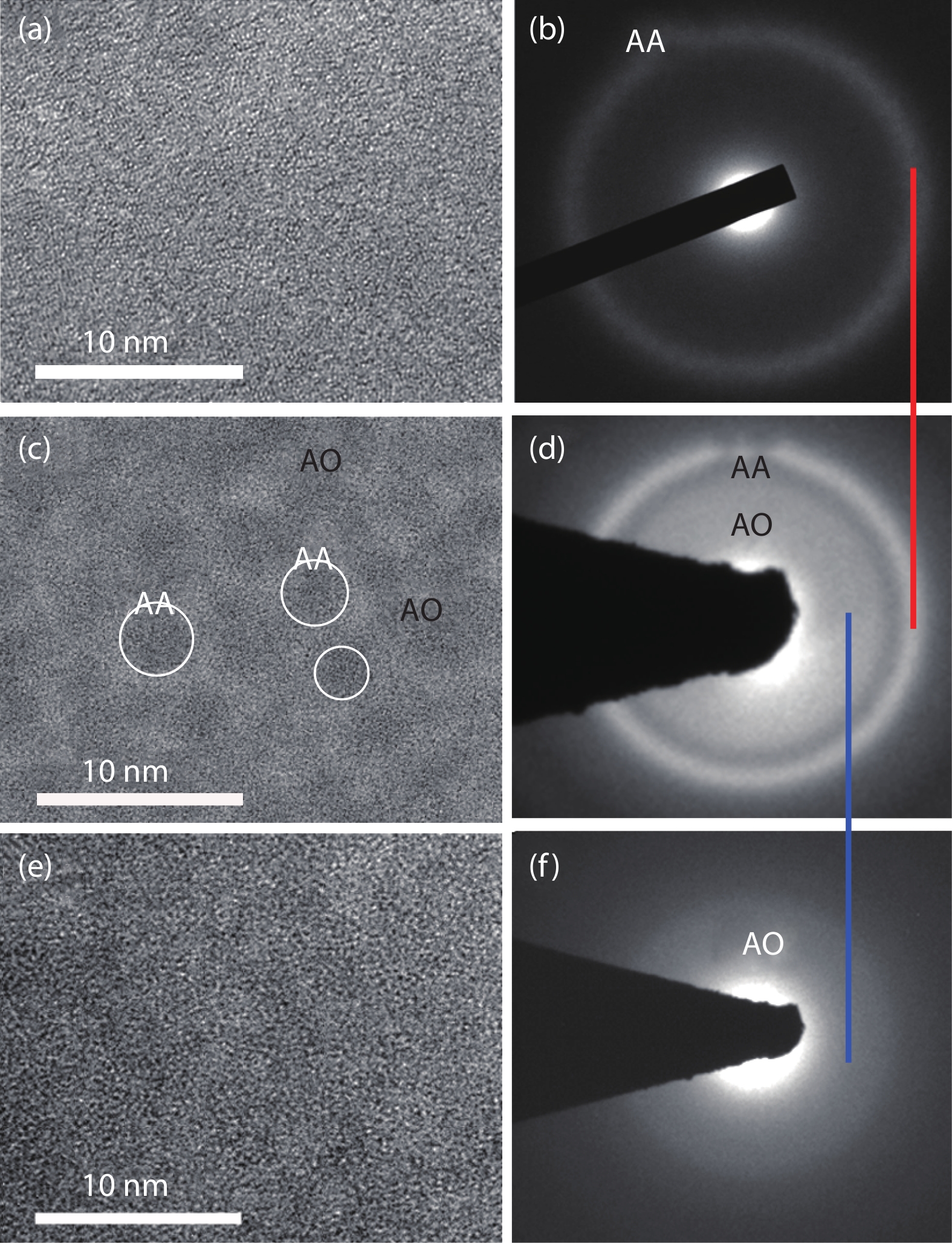
Chen N, Li H P, Hirata A, et al. Transparent magnetic semiconductor with embedded metallic glass nano-granules. Mater Design, 2017, 132, 208 doi: 10.1016/j.matdes.2017.07.010
|
| [26] |
Liu W J, Zhang H X, Shi J A, et al. A room-temperature magnetic semiconductor from a ferromagnetic metallic glass. Nat Commun, 2016, 7, 13497 doi: 10.1038/ncomms13497
|
| [27] |
Inoue A. Stabilization of metallic supercooled liquid and bulk amorphous alloys. Acta Mater, 2000, 48, 279 doi: 10.1016/S1359-6454(99)00300-6
|
| [28] |
Johnson W L. Bulk glass-forming metallic alloys: science and technology. MRS Bull, 1999, 24, 42 doi: 10.1557/S0883769400053252
|
| [29] |
Greer A L. Metallic glasses. Science, 1995, 267, 1947 doi: 10.1126/science.267.5206.1947
|
| [30] |
Wang W H, Dong C, Shek C H. Bulk metallic glasses. Mater Sci Eng R, 2004, 44, 45 doi: 10.1016/j.mser.2004.03.001
|
| [31] |
Chen M W. A brief overview of bulk metallic glasses. NPG Asia Mater, 2011, 3, 82 doi: 10.1038/asiamat.2011.30
|
| [32] |
Coey J M D, Venkatesan M, Fitzgerald C B. Donor impurity band exchange in dilute ferromagnetic oxides. Nat Mater, 2005, 4, 173 doi: 10.1038/nmat1310
|
| [33] |
Inoue A, Shen B L, Koshiba H, et al. Ultra-high strength above 5000 MPa and soft magnetic properties of Co–Fe–Ta–B bulk glassy alloys. Acta Mater, 2004, 52, 1631 doi: 10.1016/j.actamat.2003.12.008
|
| [34] |
Inoue A, Shen B L, Koshiba H, et al. Cobalt-based bulk glassy alloy with ultrahigh strength and soft magnetic properties. Nat Mater, 2003, 2, 661 doi: 10.1038/nmat982
|
| [35] |
Sharma P, Kimura H, Inoue A. Observation of unusual magnetic behavior: spin reorientation transition in thick Co–Fe–Ta–B glassy films. J Appl Phys, 2006, 100, 083902 doi: 10.1063/1.2359142
|
| [36] |
Sharma P, Kimura H, Inoue A, et al. Temperature and thickness driven spin-reorientation transition in amorphous Co–Fe–Ta–B thin films. Phys Rev B, 2006, 73, 052401 doi: 10.1103/PhysRevB.73.052401
|
| [37] |
Lucas M S, Bourne W C, Sheets A O, et al. Nanocrystalline Hf and Ta containing FeCo based alloys for high frequency applications. Mater Sci Eng B, 2011, 176, 1079 doi: 10.1016/j.mseb.2011.05.044
|
| [38] |
Pellegren J P, Sokalski V M. Thickness and interface-dependent crystallization of CoFeB alloy thin films. IEEE Trans Magn, 2015, 51, 3400903 doi: 10.1109/TMAG.2015.2435798
|
| [39] |
Bader S D, Parkin S S P. Spintronics. Ann Rev Condens Matter Phys, 2010, 1, 71 doi: 10.1146/annurev-conmatphys-070909-104123
|
| [40] |
Ohno H, Chiba D, Matsukura F, et al. Electric-field control of ferromagnetism. Nature, 2000, 408, 944 doi: 10.1038/35050040
|
| [41] |
Song C, Cui B, Li F, et al. Recent progress in voltage control of magnetism: materials, mechanisms, and performance. Prog Mater Sci, 2017, 87, 33 doi: 10.1016/j.pmatsci.2017.02.002
|
| [42] |
Žutić I, Fabian J, Das Sarma S. Spintronics: fundamentals and applications. Rev Mod Phys, 2004, 76, 323 doi: 10.1103/RevModPhys.76.323
|
| [43] |
Hellman F, Hoffmann A, Tserkovnyak Y, et al. Interface-induced phenomena in magnetism. Rev Mod Phys, 2017, 89, 025006 doi: 10.1103/RevModPhys.89.025006
|
| [44] |
Awschalom D D, Flatté M E. Challenges for semiconductor spintronics. Nat Phys, 2007, 3, 153 doi: 10.1038/nphys551
|
| [45] |
Weisheit M, Fähler S, Marty A, et al. Electric field-induced modification of magnetism in thin-film ferromagnets. Science, 2007, 315, 349 doi: 10.1126/science.1136629
|
| [46] |
Cui B, Song C, Mao H J, et al. Manipulation of electric field effect by orbital switch. Adv Funct Mater, 2016, 26, 753 doi: 10.1002/adfm.201504036
|
| [47] |
Cui B, Song C, Wang G Y, et al. Reversible ferromagnetic phase transition in electrode-gated manganites. Adv Funct Mater, 2014, 24, 7233 doi: 10.1002/adfm.201402007
|
| [48] |
Yamada Y, Ueno K, Fukumura T, et al. Electrically induced ferromagnetism at room temperature in cobalt-doped titanium dioxide. Science, 2011, 332, 1065 doi: 10.1126/science.1202152
|
| [49] |
Zhang Y Q, Zhao S F, Song C, et al. Electric-field control of ferromagnetism in a Co–Fe–Ta–B amorphous alloy. Mater Design, 2018, 143, 65 doi: 10.1016/j.matdes.2018.01.046
|
| [50] |
Zhang S, Zhao Y G, Xiao X, et al. Giant electrical modulation of magnetization in Co40Fe40B20/ Pb(Mg1/3Nb2/3)0.7Ti0.3O3 (011) heterostructure. Sci Rep, 2014, 4, 3727 doi: 10.1038/srep03727
|
| [51] |
Liu Y T, Agnus G, Ono S, et al. Ionic-liquid gating of perpendicularly magnetised CoFeB/MgO thin films. J Appl Phys, 2016, 120, 023901 doi: 10.1063/1.4956433
|
| [52] |
Nakano M, Shibuya K, Okuyama D, et al. Collective bulk carrier delocalization driven by electrostatic surface charge accumulation. Nature, 2012, 487, 459 doi: 10.1038/nature11296
|
| [53] |
Narushima S, Mizoguchi H, Shimizu K, et al. A p-type amorphous oxide semiconductor and room temperature fabrication of amorphous oxide p–n heterojunction diodes. Adv Mater, 2003, 15, 1409 doi: 10.1002/(ISSN)1521-4095
|

| [1] |
Holtzberg F, McGuire T R, Methfessel S, et al. Effect of electron concentration on magnetic exchange interactions in rare earth chalcogenides. Phys Rev Lett, 1964, 13, 18 doi: 10.1103/PhysRevLett.13.18
|
| [2] |
Kasuya T, Yanase A. Anomalous transport phenomena in Eu-chalcogenide alloys. Rev Mod Phys, 1968, 40, 684 doi: 10.1103/RevModPhys.40.684
|
| [3] |
Methfessel S. Potential applications of magnetic rare earth compounds. IEEE Trans Mag, 1965, 1, 144 doi: 10.1109/TMAG.1965.1062951
|
| [4] |
Furdyna J K, Kossut J. Diluted magnetic semicondcutors. Vol. 25. In: Semiconductor and semimetals. New York: Academic Press, 1988
|
| [5] |
Dietl T, Ohno H. Dilute ferromagnetic semiconductors: physics and spintronic structures. Rev Mod Phys, 2014, 86, 187 doi: 10.1103/RevModPhys.86.187
|
| [6] |
Ohno H. Making nonmagnetic semiconductors ferromagnetic. Science, 1998, 281, 951 doi: 10.1126/science.281.5379.951
|
| [7] |
Ohno H, Shen A, Matsukura F, et al. (Ga,Mn)As: A new diluted magnetic semiconductor based on GaAs. Appl Phys Lett, 1996, 69, 363 doi: 10.1063/1.118061
|
| [8] |
Munekata H, Ohno H, von Molnár S, et al. Diluted magnetic III–V semiconductors. Phys Rev Lett, 1989, 63, 1849 doi: 10.1103/PhysRevLett.63.1849
|
| [9] |
Chen L, Yang X, Yang F H, et al. Enhancing the Curie temperature of ferromagnetic semiconductor (Ga,Mn)As to 200 K via nanostructure engineering. Nano Lett, 2011, 11, 2584 doi: 10.1021/nl201187m
|
| [10] |
Matsumoto Y, Murakami M, Shono T, et al. Room-temperature ferromagnetism in transparent transition metal-doped titanium dioxide. Science, 2001, 291, 854 doi: 10.1126/science.1056186
|
| [11] |
Pulizzi F, Chambers S. Is it really intrinsic ferromagnetism. Nat Mater, 2010, 9, 956 doi: 10.1038/nmat2905
|
| [12] |
Chen L, Yan S, Xu P F, et al. Low-temperature magnetotransport behaviors of heavily Mn-doped (Ga,Mn)As films with high ferromagnetic transition temperature. Appl Phys Lett, 2009, 95, 182505 doi: 10.1063/1.3259821
|
| [13] |
Pulizzi F, Samarth N. A model ferromagnetic semiconductor. Nat Mater, 2010, 9, 955 doi: 10.1038/nmat2908
|
| [14] |
Ohno H. A window on the future of spintronics. Nat Mater, 2010, 9, 952 doi: 10.1038/nmat2913
|
| [15] |
Wang X L, Wang H L, Pan D, et al. Robust manipulation of magnetism in dilute magnetic semiconductor (Ga,Mn)As by organic molecules. Adv Mater, 2015, 27, 8043 doi: 10.1002/adma.201503547
|
| [16] |
Editorial. More than just room temperature. Nat Mater, 2010, 9, 951 doi: 10.1038/nmat2918
|
| [17] |
Nie S H, Chin Y Y, Liu W Q, et al. Ferromagnetic interfacial interaction and the proximity effect in a Co2FeAl/(Ga,Mn)As bilayer. Phys Rev Lett, 2013, 111, 027203 doi: 10.1103/PhysRevLett.111.027203
|
| [18] |
Dietl T. A ten-year perspective on dilute magnetic semiconductors and oxides. Nat Mater, 2010, 9, 965 doi: 10.1038/nmat2898
|
| [19] |
Yu X Z, Wang H L, Pan D, et al. All zinc-blende GaAs/(Ga,Mn)As core-shell nanowires with ferromagnetic ordering. Nano Lett, 2013, 13, 1572 doi: 10.1021/nl304740k
|
| [20] |
Zhao J H. Is it possible to create magnetic semiconductors that work at room temperature. Chin Sci Bull, 2016, 61, 1401 doi: 10.1360/N972015-01392
|
| [21] |
Hume-Rothery W. Phase stability in metals and alloys. New York: McGraw-Hill Book Company, 1966
|
| [22] |
Hoistad L M, Lee S. The Hume-Rothery electron concentration rules and second moment scaling. J Am Chem Soc, 1991, 113, 8216 doi: 10.1021/ja00022a004
|
| [23] |
Hume-Rothery W. The structure of metals and alloys. The Institute of Metals, London, 1939
|
| [24] |
Chen N, Zhang Y Q, Yao K F. Transparent magnetic semiconductors from ferromagnetic amorphous alloys. Acta Phys Sin, 2017, 66, 176113 doi: 10.7498/aps.66.176113
|
| [25] |
Chen N, Li H P, Hirata A, et al. Transparent magnetic semiconductor with embedded metallic glass nano-granules. Mater Design, 2017, 132, 208 doi: 10.1016/j.matdes.2017.07.010
|
| [26] |
Liu W J, Zhang H X, Shi J A, et al. A room-temperature magnetic semiconductor from a ferromagnetic metallic glass. Nat Commun, 2016, 7, 13497 doi: 10.1038/ncomms13497
|
| [27] |
Inoue A. Stabilization of metallic supercooled liquid and bulk amorphous alloys. Acta Mater, 2000, 48, 279 doi: 10.1016/S1359-6454(99)00300-6
|
| [28] |
Johnson W L. Bulk glass-forming metallic alloys: science and technology. MRS Bull, 1999, 24, 42 doi: 10.1557/S0883769400053252
|
| [29] |
Greer A L. Metallic glasses. Science, 1995, 267, 1947 doi: 10.1126/science.267.5206.1947
|
| [30] |
Wang W H, Dong C, Shek C H. Bulk metallic glasses. Mater Sci Eng R, 2004, 44, 45 doi: 10.1016/j.mser.2004.03.001
|
| [31] |
Chen M W. A brief overview of bulk metallic glasses. NPG Asia Mater, 2011, 3, 82 doi: 10.1038/asiamat.2011.30
|
| [32] |
Coey J M D, Venkatesan M, Fitzgerald C B. Donor impurity band exchange in dilute ferromagnetic oxides. Nat Mater, 2005, 4, 173 doi: 10.1038/nmat1310
|
| [33] |
Inoue A, Shen B L, Koshiba H, et al. Ultra-high strength above 5000 MPa and soft magnetic properties of Co–Fe–Ta–B bulk glassy alloys. Acta Mater, 2004, 52, 1631 doi: 10.1016/j.actamat.2003.12.008
|
| [34] |
Inoue A, Shen B L, Koshiba H, et al. Cobalt-based bulk glassy alloy with ultrahigh strength and soft magnetic properties. Nat Mater, 2003, 2, 661 doi: 10.1038/nmat982
|
| [35] |
Sharma P, Kimura H, Inoue A. Observation of unusual magnetic behavior: spin reorientation transition in thick Co–Fe–Ta–B glassy films. J Appl Phys, 2006, 100, 083902 doi: 10.1063/1.2359142
|
| [36] |
Sharma P, Kimura H, Inoue A, et al. Temperature and thickness driven spin-reorientation transition in amorphous Co–Fe–Ta–B thin films. Phys Rev B, 2006, 73, 052401 doi: 10.1103/PhysRevB.73.052401
|
| [37] |
Lucas M S, Bourne W C, Sheets A O, et al. Nanocrystalline Hf and Ta containing FeCo based alloys for high frequency applications. Mater Sci Eng B, 2011, 176, 1079 doi: 10.1016/j.mseb.2011.05.044
|
| [38] |
Pellegren J P, Sokalski V M. Thickness and interface-dependent crystallization of CoFeB alloy thin films. IEEE Trans Magn, 2015, 51, 3400903 doi: 10.1109/TMAG.2015.2435798
|
| [39] |
Bader S D, Parkin S S P. Spintronics. Ann Rev Condens Matter Phys, 2010, 1, 71 doi: 10.1146/annurev-conmatphys-070909-104123
|
| [40] |
Ohno H, Chiba D, Matsukura F, et al. Electric-field control of ferromagnetism. Nature, 2000, 408, 944 doi: 10.1038/35050040
|
| [41] |
Song C, Cui B, Li F, et al. Recent progress in voltage control of magnetism: materials, mechanisms, and performance. Prog Mater Sci, 2017, 87, 33 doi: 10.1016/j.pmatsci.2017.02.002
|
| [42] |
Žutić I, Fabian J, Das Sarma S. Spintronics: fundamentals and applications. Rev Mod Phys, 2004, 76, 323 doi: 10.1103/RevModPhys.76.323
|
| [43] |
Hellman F, Hoffmann A, Tserkovnyak Y, et al. Interface-induced phenomena in magnetism. Rev Mod Phys, 2017, 89, 025006 doi: 10.1103/RevModPhys.89.025006
|
| [44] |
Awschalom D D, Flatté M E. Challenges for semiconductor spintronics. Nat Phys, 2007, 3, 153 doi: 10.1038/nphys551
|
| [45] |
Weisheit M, Fähler S, Marty A, et al. Electric field-induced modification of magnetism in thin-film ferromagnets. Science, 2007, 315, 349 doi: 10.1126/science.1136629
|
| [46] |
Cui B, Song C, Mao H J, et al. Manipulation of electric field effect by orbital switch. Adv Funct Mater, 2016, 26, 753 doi: 10.1002/adfm.201504036
|
| [47] |
Cui B, Song C, Wang G Y, et al. Reversible ferromagnetic phase transition in electrode-gated manganites. Adv Funct Mater, 2014, 24, 7233 doi: 10.1002/adfm.201402007
|
| [48] |
Yamada Y, Ueno K, Fukumura T, et al. Electrically induced ferromagnetism at room temperature in cobalt-doped titanium dioxide. Science, 2011, 332, 1065 doi: 10.1126/science.1202152
|
| [49] |
Zhang Y Q, Zhao S F, Song C, et al. Electric-field control of ferromagnetism in a Co–Fe–Ta–B amorphous alloy. Mater Design, 2018, 143, 65 doi: 10.1016/j.matdes.2018.01.046
|
| [50] |
Zhang S, Zhao Y G, Xiao X, et al. Giant electrical modulation of magnetization in Co40Fe40B20/ Pb(Mg1/3Nb2/3)0.7Ti0.3O3 (011) heterostructure. Sci Rep, 2014, 4, 3727 doi: 10.1038/srep03727
|
| [51] |
Liu Y T, Agnus G, Ono S, et al. Ionic-liquid gating of perpendicularly magnetised CoFeB/MgO thin films. J Appl Phys, 2016, 120, 023901 doi: 10.1063/1.4956433
|
| [52] |
Nakano M, Shibuya K, Okuyama D, et al. Collective bulk carrier delocalization driven by electrostatic surface charge accumulation. Nature, 2012, 487, 459 doi: 10.1038/nature11296
|
| [53] |
Narushima S, Mizoguchi H, Shimizu K, et al. A p-type amorphous oxide semiconductor and room temperature fabrication of amorphous oxide p–n heterojunction diodes. Adv Mater, 2003, 15, 1409 doi: 10.1002/(ISSN)1521-4095
|


Article views: 5403 Times PDF downloads: 163 Times Cited by: 0 Times
Received: 03 June 2019 Revised: 14 June 2019 Online: Accepted Manuscript: 04 July 2019Uncorrected proof: 08 July 2019Published: 09 August 2019
| Citation: |
Na Chen, Kaixuan Fang, Hongxia Zhang, Yingqi Zhang, Wenjian Liu, Kefu Yao, Zhengjun Zhang. Amorphous magnetic semiconductors with Curie temperatures above room temperature[J]. Journal of Semiconductors, 2019, 40(8): 081510. doi: 10.1088/1674-4926/40/8/081510
****
N Chen, K X Fang, H X Zhang, Y Q Zhang, W J Liu, K F Yao, Z J Zhang, Amorphous magnetic semiconductors with Curie temperatures above room temperature[J]. J. Semicond., 2019, 40(8): 081510. doi: 10.1088/1674-4926/40/8/081510.

|
| [1] |
Holtzberg F, McGuire T R, Methfessel S, et al. Effect of electron concentration on magnetic exchange interactions in rare earth chalcogenides. Phys Rev Lett, 1964, 13, 18 doi: 10.1103/PhysRevLett.13.18
|
| [2] |
Kasuya T, Yanase A. Anomalous transport phenomena in Eu-chalcogenide alloys. Rev Mod Phys, 1968, 40, 684 doi: 10.1103/RevModPhys.40.684
|
| [3] |
Methfessel S. Potential applications of magnetic rare earth compounds. IEEE Trans Mag, 1965, 1, 144 doi: 10.1109/TMAG.1965.1062951
|
| [4] |
Furdyna J K, Kossut J. Diluted magnetic semicondcutors. Vol. 25. In: Semiconductor and semimetals. New York: Academic Press, 1988
|
| [5] |
Dietl T, Ohno H. Dilute ferromagnetic semiconductors: physics and spintronic structures. Rev Mod Phys, 2014, 86, 187 doi: 10.1103/RevModPhys.86.187
|
| [6] |
Ohno H. Making nonmagnetic semiconductors ferromagnetic. Science, 1998, 281, 951 doi: 10.1126/science.281.5379.951
|
| [7] |
Ohno H, Shen A, Matsukura F, et al. (Ga,Mn)As: A new diluted magnetic semiconductor based on GaAs. Appl Phys Lett, 1996, 69, 363 doi: 10.1063/1.118061
|
| [8] |
Munekata H, Ohno H, von Molnár S, et al. Diluted magnetic III–V semiconductors. Phys Rev Lett, 1989, 63, 1849 doi: 10.1103/PhysRevLett.63.1849
|
| [9] |
Chen L, Yang X, Yang F H, et al. Enhancing the Curie temperature of ferromagnetic semiconductor (Ga,Mn)As to 200 K via nanostructure engineering. Nano Lett, 2011, 11, 2584 doi: 10.1021/nl201187m
|
| [10] |
Matsumoto Y, Murakami M, Shono T, et al. Room-temperature ferromagnetism in transparent transition metal-doped titanium dioxide. Science, 2001, 291, 854 doi: 10.1126/science.1056186
|
| [11] |
Pulizzi F, Chambers S. Is it really intrinsic ferromagnetism. Nat Mater, 2010, 9, 956 doi: 10.1038/nmat2905
|
| [12] |
Chen L, Yan S, Xu P F, et al. Low-temperature magnetotransport behaviors of heavily Mn-doped (Ga,Mn)As films with high ferromagnetic transition temperature. Appl Phys Lett, 2009, 95, 182505 doi: 10.1063/1.3259821
|
| [13] |
Pulizzi F, Samarth N. A model ferromagnetic semiconductor. Nat Mater, 2010, 9, 955 doi: 10.1038/nmat2908
|
| [14] |
Ohno H. A window on the future of spintronics. Nat Mater, 2010, 9, 952 doi: 10.1038/nmat2913
|
| [15] |
Wang X L, Wang H L, Pan D, et al. Robust manipulation of magnetism in dilute magnetic semiconductor (Ga,Mn)As by organic molecules. Adv Mater, 2015, 27, 8043 doi: 10.1002/adma.201503547
|
| [16] |
Editorial. More than just room temperature. Nat Mater, 2010, 9, 951 doi: 10.1038/nmat2918
|
| [17] |
Nie S H, Chin Y Y, Liu W Q, et al. Ferromagnetic interfacial interaction and the proximity effect in a Co2FeAl/(Ga,Mn)As bilayer. Phys Rev Lett, 2013, 111, 027203 doi: 10.1103/PhysRevLett.111.027203
|
| [18] |
Dietl T. A ten-year perspective on dilute magnetic semiconductors and oxides. Nat Mater, 2010, 9, 965 doi: 10.1038/nmat2898
|
| [19] |
Yu X Z, Wang H L, Pan D, et al. All zinc-blende GaAs/(Ga,Mn)As core-shell nanowires with ferromagnetic ordering. Nano Lett, 2013, 13, 1572 doi: 10.1021/nl304740k
|
| [20] |
Zhao J H. Is it possible to create magnetic semiconductors that work at room temperature. Chin Sci Bull, 2016, 61, 1401 doi: 10.1360/N972015-01392
|
| [21] |
Hume-Rothery W. Phase stability in metals and alloys. New York: McGraw-Hill Book Company, 1966
|
| [22] |
Hoistad L M, Lee S. The Hume-Rothery electron concentration rules and second moment scaling. J Am Chem Soc, 1991, 113, 8216 doi: 10.1021/ja00022a004
|
| [23] |
Hume-Rothery W. The structure of metals and alloys. The Institute of Metals, London, 1939
|
| [24] |
Chen N, Zhang Y Q, Yao K F. Transparent magnetic semiconductors from ferromagnetic amorphous alloys. Acta Phys Sin, 2017, 66, 176113 doi: 10.7498/aps.66.176113
|
| [25] |
Chen N, Li H P, Hirata A, et al. Transparent magnetic semiconductor with embedded metallic glass nano-granules. Mater Design, 2017, 132, 208 doi: 10.1016/j.matdes.2017.07.010
|
| [26] |
Liu W J, Zhang H X, Shi J A, et al. A room-temperature magnetic semiconductor from a ferromagnetic metallic glass. Nat Commun, 2016, 7, 13497 doi: 10.1038/ncomms13497
|
| [27] |
Inoue A. Stabilization of metallic supercooled liquid and bulk amorphous alloys. Acta Mater, 2000, 48, 279 doi: 10.1016/S1359-6454(99)00300-6
|
| [28] |
Johnson W L. Bulk glass-forming metallic alloys: science and technology. MRS Bull, 1999, 24, 42 doi: 10.1557/S0883769400053252
|
| [29] |
Greer A L. Metallic glasses. Science, 1995, 267, 1947 doi: 10.1126/science.267.5206.1947
|
| [30] |
Wang W H, Dong C, Shek C H. Bulk metallic glasses. Mater Sci Eng R, 2004, 44, 45 doi: 10.1016/j.mser.2004.03.001
|
| [31] |
Chen M W. A brief overview of bulk metallic glasses. NPG Asia Mater, 2011, 3, 82 doi: 10.1038/asiamat.2011.30
|
| [32] |
Coey J M D, Venkatesan M, Fitzgerald C B. Donor impurity band exchange in dilute ferromagnetic oxides. Nat Mater, 2005, 4, 173 doi: 10.1038/nmat1310
|
| [33] |
Inoue A, Shen B L, Koshiba H, et al. Ultra-high strength above 5000 MPa and soft magnetic properties of Co–Fe–Ta–B bulk glassy alloys. Acta Mater, 2004, 52, 1631 doi: 10.1016/j.actamat.2003.12.008
|
| [34] |
Inoue A, Shen B L, Koshiba H, et al. Cobalt-based bulk glassy alloy with ultrahigh strength and soft magnetic properties. Nat Mater, 2003, 2, 661 doi: 10.1038/nmat982
|
| [35] |
Sharma P, Kimura H, Inoue A. Observation of unusual magnetic behavior: spin reorientation transition in thick Co–Fe–Ta–B glassy films. J Appl Phys, 2006, 100, 083902 doi: 10.1063/1.2359142
|
| [36] |
Sharma P, Kimura H, Inoue A, et al. Temperature and thickness driven spin-reorientation transition in amorphous Co–Fe–Ta–B thin films. Phys Rev B, 2006, 73, 052401 doi: 10.1103/PhysRevB.73.052401
|
| [37] |
Lucas M S, Bourne W C, Sheets A O, et al. Nanocrystalline Hf and Ta containing FeCo based alloys for high frequency applications. Mater Sci Eng B, 2011, 176, 1079 doi: 10.1016/j.mseb.2011.05.044
|
| [38] |
Pellegren J P, Sokalski V M. Thickness and interface-dependent crystallization of CoFeB alloy thin films. IEEE Trans Magn, 2015, 51, 3400903 doi: 10.1109/TMAG.2015.2435798
|
| [39] |
Bader S D, Parkin S S P. Spintronics. Ann Rev Condens Matter Phys, 2010, 1, 71 doi: 10.1146/annurev-conmatphys-070909-104123
|
| [40] |
Ohno H, Chiba D, Matsukura F, et al. Electric-field control of ferromagnetism. Nature, 2000, 408, 944 doi: 10.1038/35050040
|
| [41] |
Song C, Cui B, Li F, et al. Recent progress in voltage control of magnetism: materials, mechanisms, and performance. Prog Mater Sci, 2017, 87, 33 doi: 10.1016/j.pmatsci.2017.02.002
|
| [42] |
Žutić I, Fabian J, Das Sarma S. Spintronics: fundamentals and applications. Rev Mod Phys, 2004, 76, 323 doi: 10.1103/RevModPhys.76.323
|
| [43] |
Hellman F, Hoffmann A, Tserkovnyak Y, et al. Interface-induced phenomena in magnetism. Rev Mod Phys, 2017, 89, 025006 doi: 10.1103/RevModPhys.89.025006
|
| [44] |
Awschalom D D, Flatté M E. Challenges for semiconductor spintronics. Nat Phys, 2007, 3, 153 doi: 10.1038/nphys551
|
| [45] |
Weisheit M, Fähler S, Marty A, et al. Electric field-induced modification of magnetism in thin-film ferromagnets. Science, 2007, 315, 349 doi: 10.1126/science.1136629
|
| [46] |
Cui B, Song C, Mao H J, et al. Manipulation of electric field effect by orbital switch. Adv Funct Mater, 2016, 26, 753 doi: 10.1002/adfm.201504036
|
| [47] |
Cui B, Song C, Wang G Y, et al. Reversible ferromagnetic phase transition in electrode-gated manganites. Adv Funct Mater, 2014, 24, 7233 doi: 10.1002/adfm.201402007
|
| [48] |
Yamada Y, Ueno K, Fukumura T, et al. Electrically induced ferromagnetism at room temperature in cobalt-doped titanium dioxide. Science, 2011, 332, 1065 doi: 10.1126/science.1202152
|
| [49] |
Zhang Y Q, Zhao S F, Song C, et al. Electric-field control of ferromagnetism in a Co–Fe–Ta–B amorphous alloy. Mater Design, 2018, 143, 65 doi: 10.1016/j.matdes.2018.01.046
|
| [50] |
Zhang S, Zhao Y G, Xiao X, et al. Giant electrical modulation of magnetization in Co40Fe40B20/ Pb(Mg1/3Nb2/3)0.7Ti0.3O3 (011) heterostructure. Sci Rep, 2014, 4, 3727 doi: 10.1038/srep03727
|
| [51] |
Liu Y T, Agnus G, Ono S, et al. Ionic-liquid gating of perpendicularly magnetised CoFeB/MgO thin films. J Appl Phys, 2016, 120, 023901 doi: 10.1063/1.4956433
|
| [52] |
Nakano M, Shibuya K, Okuyama D, et al. Collective bulk carrier delocalization driven by electrostatic surface charge accumulation. Nature, 2012, 487, 459 doi: 10.1038/nature11296
|
| [53] |
Narushima S, Mizoguchi H, Shimizu K, et al. A p-type amorphous oxide semiconductor and room temperature fabrication of amorphous oxide p–n heterojunction diodes. Adv Mater, 2003, 15, 1409 doi: 10.1002/(ISSN)1521-4095
|

 WeChat ID
Journal of Semiconductors © 2017 All Rights Reserved 京ICP备05085259号-2

 DownLoad:

