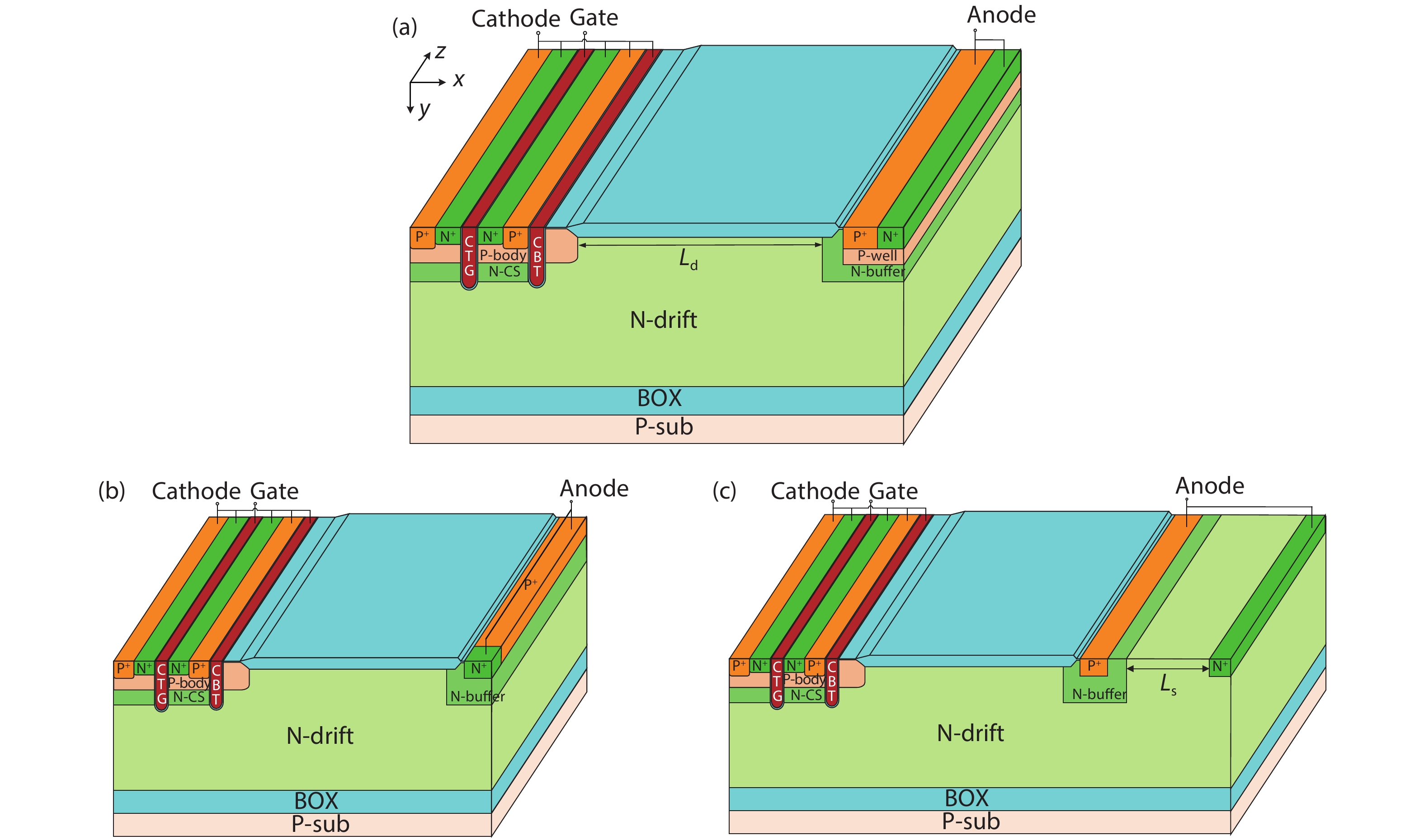
Fig. 1.
(Color online) Schematic cross-sectional views of (a) DT-NPN LIGBT, (b) SEG LTIGBT, and (c) SSA LTIGBT.
ARTICLES
Chenxia Wang, Jie Wei, Diao Fan, Yang Yang and Xiaorong Luo
Corresponding author: Jie Wei, Email: weijieuestc@uestc.edu.cn; Xiaorong Luo, xrluo@uestc.edu.cn
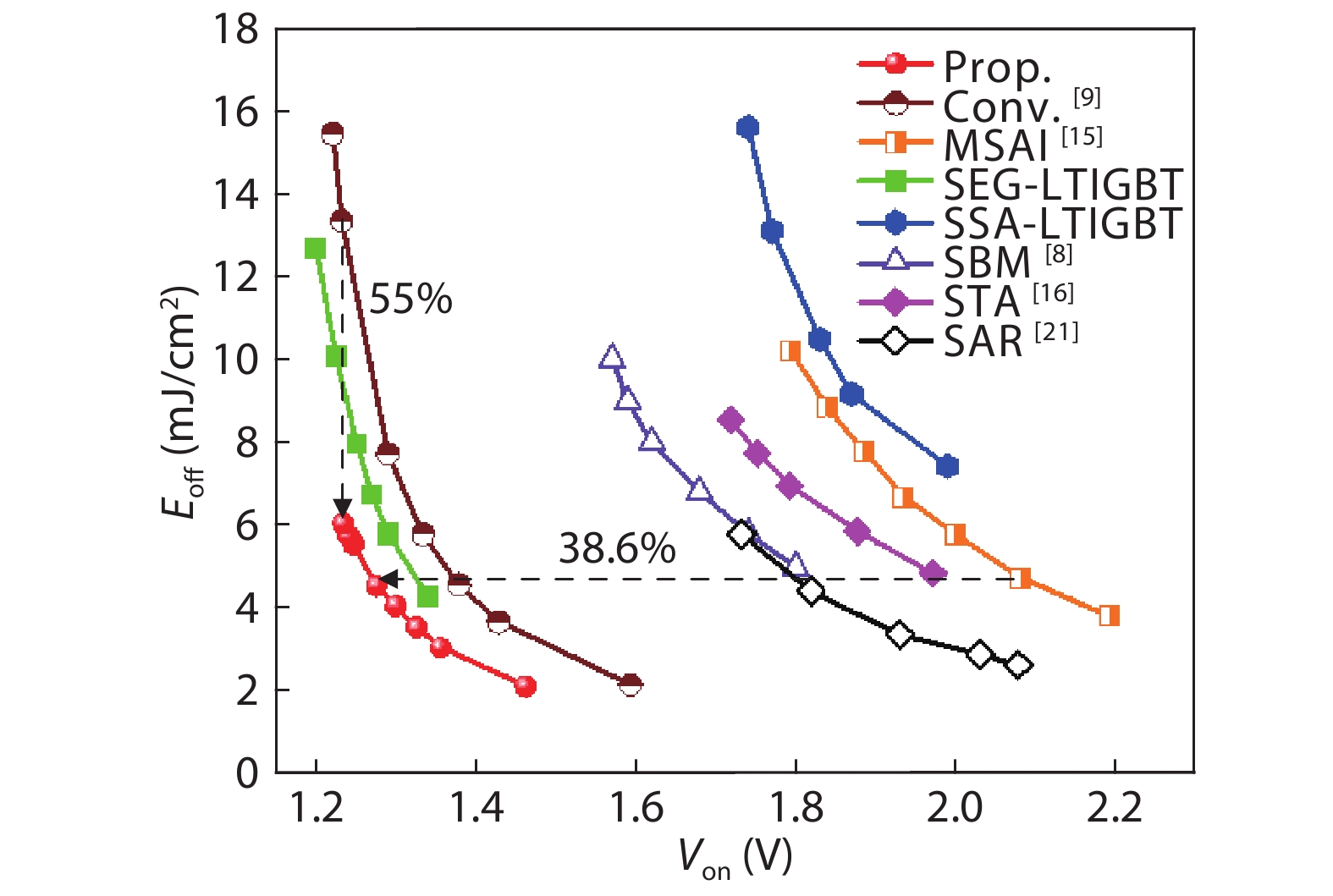
Abstract: A novel 600 V snapback-free high-speed silicon-on-insulator lateral insulated gate bipolar transistor is proposed and investigated by simulation. The proposed device features an embedded NPN structure at the anode side, and double trenches together with an N-type carrier storage (N-CS) layer at the cathode side, named DT-NPN LIGBT. The NPN structure not only acts as an electron barrier to eliminate the snapback effect in the on-state within a smaller cell pitch but also provides an extra electron extracting path during the turn-off stage to decrease the turnoff loss (Eoff). The double cathode trenches and N-CS layer hinder the hole from being extracted by the cathode quickly. They then enhance carrier storing effect and lead to a reduced on-state voltage drop (Von). The latch-up immunity is improved by the double cathode trenches. Hence, the DT-NPN LIGBT obtains a superior tradeoff between the Von and Eoff. Additionally, the DT-NPN LIGBT exhibits an improved blocking capability and weak dependence of breakdown voltage (BV) on the P+ anode doping concentration because the NPN structure suppresses triggering the PNP transistor. The proposed LIGBT reduces the Eoff by 55% at the same Von, and improves the BV by 7.3% compared to the conventional LIGBT.
Keywords: snapback-free, fast switching, SOI LIGBT, trench gate, Eoff
| [1] |
Iwamuro N, Laska T. IGBT history, state-of-the-art, and future prospects. IEEE Trans Electron Devices, 2017, 64, 741 doi: 10.1109/TED.2017.2654599
|
| [2] |
Disney D, Letavic T, Trajkovic T, et al. High-voltage integrated circuits: History, state of the art, and future prospects. IEEE Trans Electron Devices, 2017, 64, 659 doi: 10.1109/TED.2016.2631125
|
| [3] |
Hu H, Huang H M, Chen X B. A novel double-RESURF SOI lateral TIGBT with self-biased nMOS for improved VCE(sat)–Eoff tradeoff relationship. IEEE Trans Electron Devices, 2019, 66, 814 doi: 10.1109/TED.2018.2878474
|
| [4] |
Green D W, Sweet M, Vershinin K V, et al. Performance analysis of the segment npn anode LIGBT. IEEE Trans Electron Devices, 2005, 52, 2482 doi: 10.1109/TED.2005.857168
|
| [5] |
Chen W S, Zhang B, Li Z J. Area-efficient fast-speed lateral IGBT with a 3-D n-region-controlled anode. IEEE Electron Device Lett, 2010, 31, 467 doi: 10.1109/LED.2010.2043638
|
| [6] |
Sun W F, Zhu J, Yang Z, et al. A composite structure named self-adjusted conductivity modulation SOI-LIGBT with low on-state voltage. 2017 29th International Symposium on Power Semiconductor Devices and IC's (ISPSD), 2017, 85
|
| [7] |
Duan B X, Sun L C, Yang Y T. Analysis of the novel snapback-free LIGBT with fast-switching and improved latch-up immunity by TCAD simulation. IEEE Electron Device Lett, 2019, 40, 63 doi: 10.1109/LED.2018.2881289
|
| [8] |
Luo X R, Zhao Z Y, Huang L H, et al. A snapback-free fast-switching SOI LIGBT with an embedded self-biased n-MOS. IEEE Trans Electron Devices, 2018, 65, 3572 doi: 10.1109/TED.2018.2842092
|
| [9] |
Matsudai T, Kitagawa M, Nakagawa A. A trench-gate injection enhanced lateral IEGT on SOI. Proceedings of International Symposium on Power Semiconductor Devices and IC's, 1995, 141
|
| [10] |
Zhang L, Zhu J, Sun W F, et al. A U-shaped channel SOI-LIGBT with dual trenches. IEEE Trans Electron Devices, 2017, 64, 2587 doi: 10.1109/TED.2017.2696258
|
| [11] |
Zhang L, Zhu J, Sun W F, et al. Comparison of short-circuit characteristics of trench gate and planar gate U-shaped channel SOI-LIGBTs. Solid-State Electron, 2017, 135, 24 doi: 10.1016/j.sse.2017.06.009
|
| [12] |
Simpson M R. Analysis of negative differential resistance in the I–V characteristics of shorted-anode LIGBT's. IEEE Trans Electron Devices, 1991, 38, 1633 doi: 10.1109/16.85160
|
| [13] |
Chul J H, Byeon D S, Oh J K, et al. A fast-switching SOI SA-LIGBT without NDR region. 12th International Symposium on Power Semiconductor Devices & ICs, 2000, 149
|
| [14] |
Sin J K O, Mukherjee S. Lateral insulated-gate bipolar transistor (LIGBT) with a segmented anode structure. IEEE Electron Device Lett, 1991, 12, 45 doi: 10.1109/55.75699
|
| [15] |
Zhou K, Sun T, Liu Q, et al. A snapback-free shorted-anode SOI LIGHT with multi-segment anode. 2017 29th International Symposium on Power Semiconductor Devices and IC's, 2017, 315
|
| [16] |
Zhang L, Zhu J, Sun W F, et al. A high current density SOI-LIGBT with segmented trenches in the anode region for suppressing negative differential resistance regime. 2015 IEEE 27th International Symposium on Power Semiconductor Devices & IC's (ISPSD), 2015, 49
|
| [17] |
TCAD Sentaurus device manual. Synopsys, Inc., Mountain View, CA, USA, 2013
|
| [18] |
Takahashi H, Haruguchi H, Hagino H, et al. Carrier stored trench-gate bipolar transistor (CSTBT) – A novel power device for high voltage application. 8th International Symposium on Power Semiconductor Devices and ICs, 1996, 349
|
| [19] |
He Y T, Qiao M, Zhang B. Ultralow turnoff loss dual-gate SOI LIGBT with trench gate barrier and carrier stored layer. Chin Phys B, 2016, 25, 127304 doi: 10.1088/1674-1056/25/12/127304
|
| [20] |
Sun T, Luo X R, Wei J, et al. A carrier stored SOI LIGBT with ultralow ON-state voltage and high current capability. IEEE Trans Electron Devices, 2018, 65, 3365 doi: 10.1109/TED.2018.2848468
|
| [21] |
Luo X R, Yang Y, Sun T, et al. A snapback-free and low-loss shorted-anode SOI LIGBT with self-adaptive resistance. IEEE Trans Electron Devices, 2019, 66, 1390 doi: 10.1109/TED.2019.2892068
|
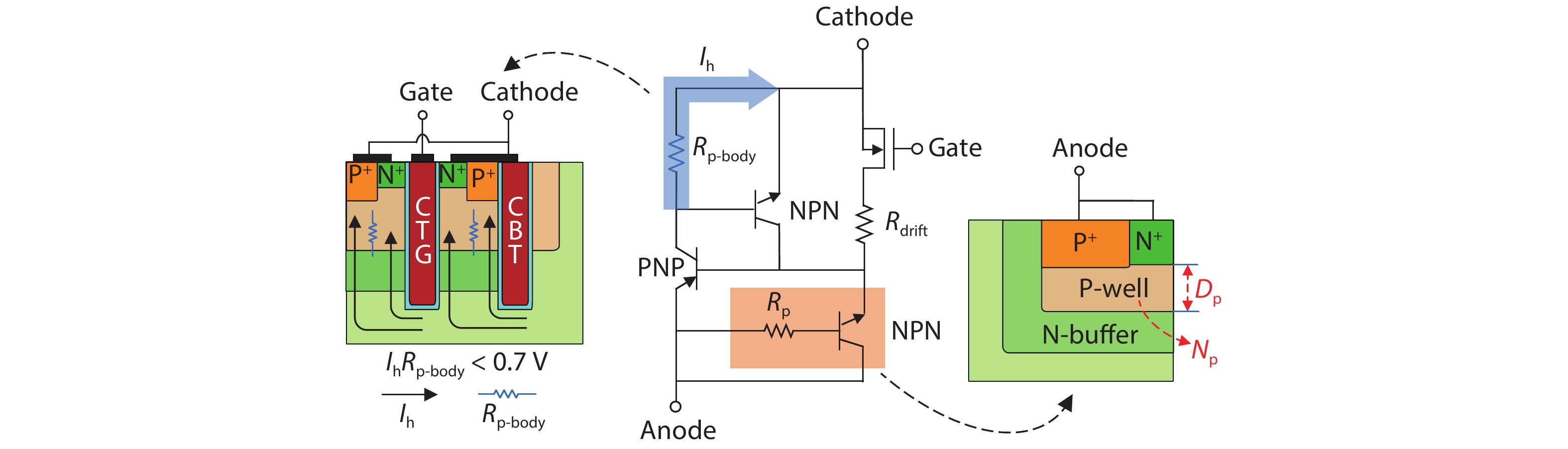
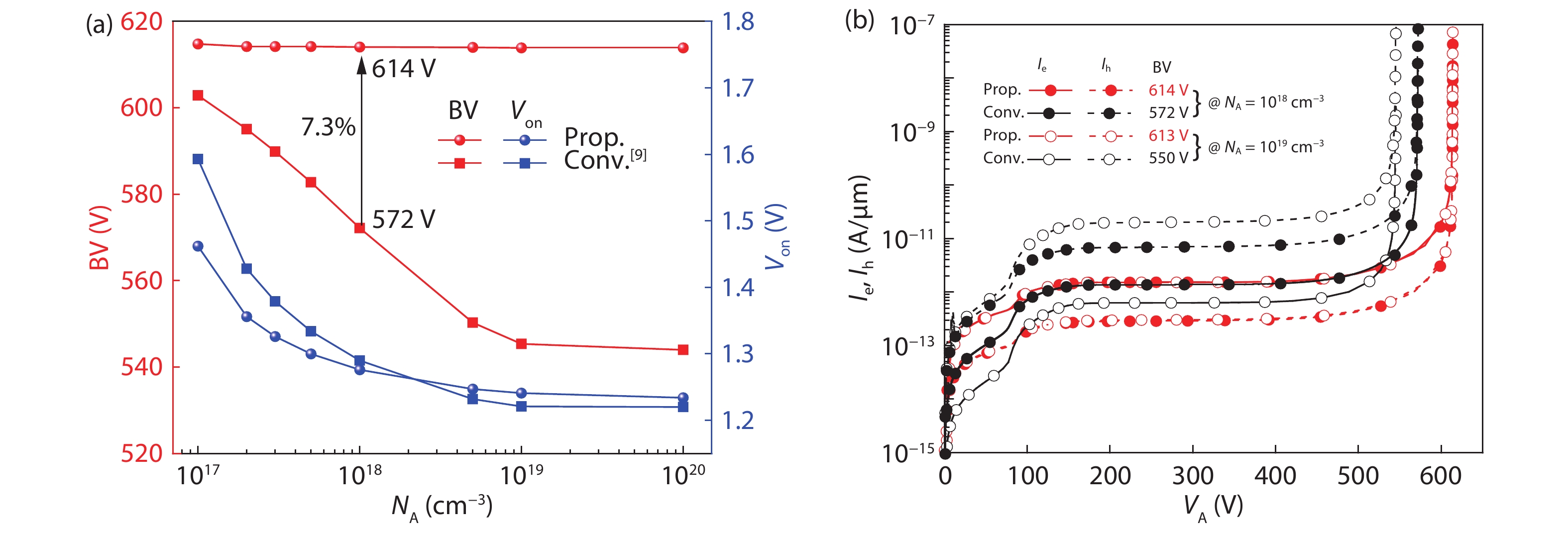
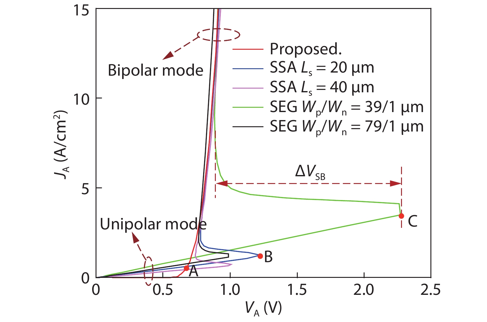
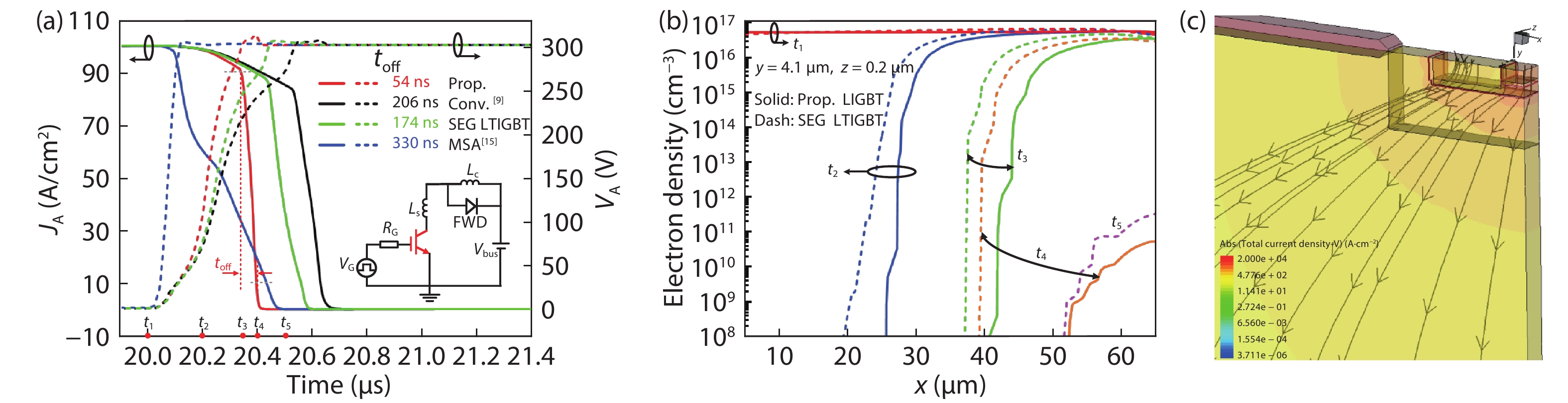
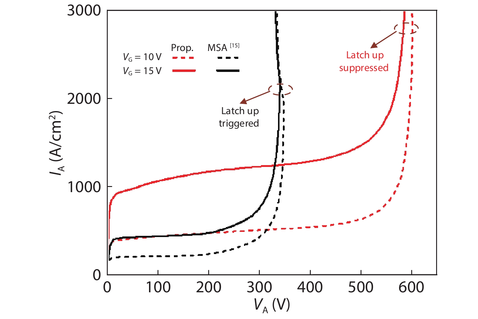
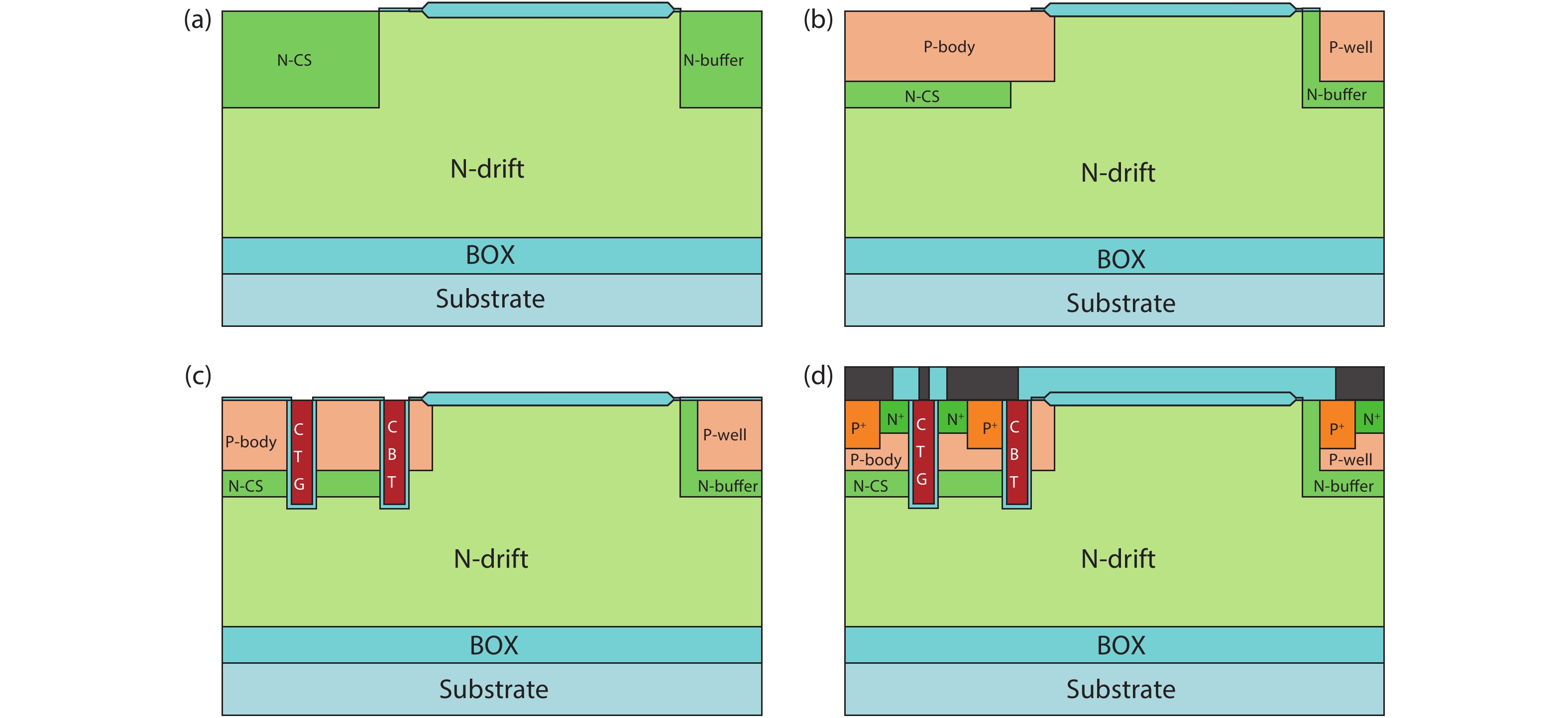
Table 1. Key parameters for LIGBTs.
| Parameter | DT-NPN | SEG | SSA |
| N-drift length, Ld (μm) | 54 | 54 | 54 |
| SOI layer thickness, Ts (μm) | 25 | 25 | 25 |
| Buried oxide thickness, tbox (μm) | 3 | 3 | 3 |
| N-drift doping, Nd (1014 cm−3) | 2 | 2 | 2 |
| N-buffer doping, Nbuffer (1016 cm−3) | 6 | 2 | 6 |
| N-CS doping, Ncs (1016 cm−3) | 6 | 6 | 6 |
| P-body doping, Np-body (1017 cm−3) | 1 | 1 | 1 |
| Gate oxide thickness (μm) | 0.1 | 0.1 | 0.1 |
| Trench depth (μm) | 4 | 4 | 4 |
 DownLoad: CSV
| [1] |
Iwamuro N, Laska T. IGBT history, state-of-the-art, and future prospects. IEEE Trans Electron Devices, 2017, 64, 741 doi: 10.1109/TED.2017.2654599
|
| [2] |
Disney D, Letavic T, Trajkovic T, et al. High-voltage integrated circuits: History, state of the art, and future prospects. IEEE Trans Electron Devices, 2017, 64, 659 doi: 10.1109/TED.2016.2631125
|
| [3] |
Hu H, Huang H M, Chen X B. A novel double-RESURF SOI lateral TIGBT with self-biased nMOS for improved VCE(sat)–Eoff tradeoff relationship. IEEE Trans Electron Devices, 2019, 66, 814 doi: 10.1109/TED.2018.2878474
|
| [4] |
Green D W, Sweet M, Vershinin K V, et al. Performance analysis of the segment npn anode LIGBT. IEEE Trans Electron Devices, 2005, 52, 2482 doi: 10.1109/TED.2005.857168
|
| [5] |
Chen W S, Zhang B, Li Z J. Area-efficient fast-speed lateral IGBT with a 3-D n-region-controlled anode. IEEE Electron Device Lett, 2010, 31, 467 doi: 10.1109/LED.2010.2043638
|
| [6] |
Sun W F, Zhu J, Yang Z, et al. A composite structure named self-adjusted conductivity modulation SOI-LIGBT with low on-state voltage. 2017 29th International Symposium on Power Semiconductor Devices and IC's (ISPSD), 2017, 85
|
| [7] |
Duan B X, Sun L C, Yang Y T. Analysis of the novel snapback-free LIGBT with fast-switching and improved latch-up immunity by TCAD simulation. IEEE Electron Device Lett, 2019, 40, 63 doi: 10.1109/LED.2018.2881289
|
| [8] |
Luo X R, Zhao Z Y, Huang L H, et al. A snapback-free fast-switching SOI LIGBT with an embedded self-biased n-MOS. IEEE Trans Electron Devices, 2018, 65, 3572 doi: 10.1109/TED.2018.2842092
|
| [9] |
Matsudai T, Kitagawa M, Nakagawa A. A trench-gate injection enhanced lateral IEGT on SOI. Proceedings of International Symposium on Power Semiconductor Devices and IC's, 1995, 141
|
| [10] |
Zhang L, Zhu J, Sun W F, et al. A U-shaped channel SOI-LIGBT with dual trenches. IEEE Trans Electron Devices, 2017, 64, 2587 doi: 10.1109/TED.2017.2696258
|
| [11] |
Zhang L, Zhu J, Sun W F, et al. Comparison of short-circuit characteristics of trench gate and planar gate U-shaped channel SOI-LIGBTs. Solid-State Electron, 2017, 135, 24 doi: 10.1016/j.sse.2017.06.009
|
| [12] |
Simpson M R. Analysis of negative differential resistance in the I–V characteristics of shorted-anode LIGBT's. IEEE Trans Electron Devices, 1991, 38, 1633 doi: 10.1109/16.85160
|
| [13] |
Chul J H, Byeon D S, Oh J K, et al. A fast-switching SOI SA-LIGBT without NDR region. 12th International Symposium on Power Semiconductor Devices & ICs, 2000, 149
|
| [14] |
Sin J K O, Mukherjee S. Lateral insulated-gate bipolar transistor (LIGBT) with a segmented anode structure. IEEE Electron Device Lett, 1991, 12, 45 doi: 10.1109/55.75699
|
| [15] |
Zhou K, Sun T, Liu Q, et al. A snapback-free shorted-anode SOI LIGHT with multi-segment anode. 2017 29th International Symposium on Power Semiconductor Devices and IC's, 2017, 315
|
| [16] |
Zhang L, Zhu J, Sun W F, et al. A high current density SOI-LIGBT with segmented trenches in the anode region for suppressing negative differential resistance regime. 2015 IEEE 27th International Symposium on Power Semiconductor Devices & IC's (ISPSD), 2015, 49
|
| [17] |
TCAD Sentaurus device manual. Synopsys, Inc., Mountain View, CA, USA, 2013
|
| [18] |
Takahashi H, Haruguchi H, Hagino H, et al. Carrier stored trench-gate bipolar transistor (CSTBT) – A novel power device for high voltage application. 8th International Symposium on Power Semiconductor Devices and ICs, 1996, 349
|
| [19] |
He Y T, Qiao M, Zhang B. Ultralow turnoff loss dual-gate SOI LIGBT with trench gate barrier and carrier stored layer. Chin Phys B, 2016, 25, 127304 doi: 10.1088/1674-1056/25/12/127304
|
| [20] |
Sun T, Luo X R, Wei J, et al. A carrier stored SOI LIGBT with ultralow ON-state voltage and high current capability. IEEE Trans Electron Devices, 2018, 65, 3365 doi: 10.1109/TED.2018.2848468
|
| [21] |
Luo X R, Yang Y, Sun T, et al. A snapback-free and low-loss shorted-anode SOI LIGBT with self-adaptive resistance. IEEE Trans Electron Devices, 2019, 66, 1390 doi: 10.1109/TED.2019.2892068
|


Article views: 5035 Times PDF downloads: 92 Times Cited by: 0 Times
Received: 02 January 2020 Revised: 04 May 2020 Online: Accepted Manuscript: 23 June 2020Uncorrected proof: 24 June 2020Published: 01 October 2020
| Citation: |
Chenxia Wang, Jie Wei, Diao Fan, Yang Yang, Xiaorong Luo. A snapback-free and high-speed SOI LIGBT with double trenches and embedded fully NPN structure[J]. Journal of Semiconductors, 2020, 41(10): 102402. doi: 10.1088/1674-4926/41/10/102402
****
C X Wang, J Wei, D Fan, Y Yang, X R Luo, A snapback-free and high-speed SOI LIGBT with double trenches and embedded fully NPN structure[J]. J. Semicond., 2020, 41(10): 102402. doi: 10.1088/1674-4926/41/10/102402.

|
| [1] |
Iwamuro N, Laska T. IGBT history, state-of-the-art, and future prospects. IEEE Trans Electron Devices, 2017, 64, 741 doi: 10.1109/TED.2017.2654599
|
| [2] |
Disney D, Letavic T, Trajkovic T, et al. High-voltage integrated circuits: History, state of the art, and future prospects. IEEE Trans Electron Devices, 2017, 64, 659 doi: 10.1109/TED.2016.2631125
|
| [3] |
Hu H, Huang H M, Chen X B. A novel double-RESURF SOI lateral TIGBT with self-biased nMOS for improved VCE(sat)–Eoff tradeoff relationship. IEEE Trans Electron Devices, 2019, 66, 814 doi: 10.1109/TED.2018.2878474
|
| [4] |
Green D W, Sweet M, Vershinin K V, et al. Performance analysis of the segment npn anode LIGBT. IEEE Trans Electron Devices, 2005, 52, 2482 doi: 10.1109/TED.2005.857168
|
| [5] |
Chen W S, Zhang B, Li Z J. Area-efficient fast-speed lateral IGBT with a 3-D n-region-controlled anode. IEEE Electron Device Lett, 2010, 31, 467 doi: 10.1109/LED.2010.2043638
|
| [6] |
Sun W F, Zhu J, Yang Z, et al. A composite structure named self-adjusted conductivity modulation SOI-LIGBT with low on-state voltage. 2017 29th International Symposium on Power Semiconductor Devices and IC's (ISPSD), 2017, 85
|
| [7] |
Duan B X, Sun L C, Yang Y T. Analysis of the novel snapback-free LIGBT with fast-switching and improved latch-up immunity by TCAD simulation. IEEE Electron Device Lett, 2019, 40, 63 doi: 10.1109/LED.2018.2881289
|
| [8] |
Luo X R, Zhao Z Y, Huang L H, et al. A snapback-free fast-switching SOI LIGBT with an embedded self-biased n-MOS. IEEE Trans Electron Devices, 2018, 65, 3572 doi: 10.1109/TED.2018.2842092
|
| [9] |
Matsudai T, Kitagawa M, Nakagawa A. A trench-gate injection enhanced lateral IEGT on SOI. Proceedings of International Symposium on Power Semiconductor Devices and IC's, 1995, 141
|
| [10] |
Zhang L, Zhu J, Sun W F, et al. A U-shaped channel SOI-LIGBT with dual trenches. IEEE Trans Electron Devices, 2017, 64, 2587 doi: 10.1109/TED.2017.2696258
|
| [11] |
Zhang L, Zhu J, Sun W F, et al. Comparison of short-circuit characteristics of trench gate and planar gate U-shaped channel SOI-LIGBTs. Solid-State Electron, 2017, 135, 24 doi: 10.1016/j.sse.2017.06.009
|
| [12] |
Simpson M R. Analysis of negative differential resistance in the I–V characteristics of shorted-anode LIGBT's. IEEE Trans Electron Devices, 1991, 38, 1633 doi: 10.1109/16.85160
|
| [13] |
Chul J H, Byeon D S, Oh J K, et al. A fast-switching SOI SA-LIGBT without NDR region. 12th International Symposium on Power Semiconductor Devices & ICs, 2000, 149
|
| [14] |
Sin J K O, Mukherjee S. Lateral insulated-gate bipolar transistor (LIGBT) with a segmented anode structure. IEEE Electron Device Lett, 1991, 12, 45 doi: 10.1109/55.75699
|
| [15] |
Zhou K, Sun T, Liu Q, et al. A snapback-free shorted-anode SOI LIGHT with multi-segment anode. 2017 29th International Symposium on Power Semiconductor Devices and IC's, 2017, 315
|
| [16] |
Zhang L, Zhu J, Sun W F, et al. A high current density SOI-LIGBT with segmented trenches in the anode region for suppressing negative differential resistance regime. 2015 IEEE 27th International Symposium on Power Semiconductor Devices & IC's (ISPSD), 2015, 49
|
| [17] |
TCAD Sentaurus device manual. Synopsys, Inc., Mountain View, CA, USA, 2013
|
| [18] |
Takahashi H, Haruguchi H, Hagino H, et al. Carrier stored trench-gate bipolar transistor (CSTBT) – A novel power device for high voltage application. 8th International Symposium on Power Semiconductor Devices and ICs, 1996, 349
|
| [19] |
He Y T, Qiao M, Zhang B. Ultralow turnoff loss dual-gate SOI LIGBT with trench gate barrier and carrier stored layer. Chin Phys B, 2016, 25, 127304 doi: 10.1088/1674-1056/25/12/127304
|
| [20] |
Sun T, Luo X R, Wei J, et al. A carrier stored SOI LIGBT with ultralow ON-state voltage and high current capability. IEEE Trans Electron Devices, 2018, 65, 3365 doi: 10.1109/TED.2018.2848468
|
| [21] |
Luo X R, Yang Y, Sun T, et al. A snapback-free and low-loss shorted-anode SOI LIGBT with self-adaptive resistance. IEEE Trans Electron Devices, 2019, 66, 1390 doi: 10.1109/TED.2019.2892068
|

 WeChat ID
Journal of Semiconductors © 2017 All Rights Reserved 京ICP备05085259号-2