ARTICLES

A 0.5–3.0 GHz SP4T RF switch with improved body self-biasing technique in 130-nm SOI CMOS

Hao Zhang1, *, Qiangsheng Cui2, *, Xu Yan1, 3, Jiahui Shi1 and Fujiang Lin1,

+ Author Affiliations

 Corresponding author: F J Lin, linfj@ustc.edu.cn

PDF

Turn off MathJax

Abstract: A single-pole four-throw (SP4T) RF switch with charge-pump-based controller is designed and implemented in a commercial 130-nm silicon-on-insulator (SOI) CMOS process. An improved body self-biasing technique based on diodes is utilized to simplify the controlling circuitry and improve the linearity. A multistack field-effect-transistor (FET) structure with body floating technique is employed to provide good power-handling capability. The proposed design demonstrates a measured input 0.1-dB compression point of 38.5 dBm at 1.9 GHz, an insertion loss of 0.27 dB/0.33 dB and an isolation of 35 dB/27 dB at 900 MHz/1.9 GHz, respectively. The overall chip area is only 0.49 mm2. This RF switch can be used in GSM/WCDMA/LTE front-end modules.

Key words: RF switchsilicon-on-insulatorbody self-biasing techniquemultistack FETs


[1]
Yan X, Li Y, Chen Y, et al. A LNA-merged RF front-end with digitally assisted technique for gain flatness and input-match compensation. Analog Integr Circuits Signal Process, 2019, 101, 219 doi: 10.1007/s10470-019-01539-2
[2]
Zhang H, Yan X, Shi J H, et al. A 0.5–5.6 GHz inductorless wideband LNA with local active feedback. 2018 IEEE 3rd International Conference on Integrated Circuits and Microsystems (ICICM), 2018, 164
[3]
Yan X, Chen C, Yang L, et al. A 0.1–1.1 GHz inductorless differential LNA with double gm -boosting and positive feedback. Analog Integr Circuits Signal Process, 2017, 93, 205 doi: 10.1007/s10470-017-1043-y
[4]
Huang C W P, Christainsen K, Nabokin S, et al. A highly integrated single chip 5–6 GHz front-end IC based on SiGe BiCMOS that enhances 802.11ac WLAN radio front-end designs. 2015 IEEE Radio Freq Integr Circuits Symp RFIC, 2015, 227
[5]
Im D, Kim B K, Im D K, et al. A stacked-FET linear SOI CMOS cellular antenna switch with an extremely low-power biasing strategy. IEEE Trans Microw Theory Tech, 2015, 63, 1964 doi: 10.1109/TMTT.2015.2427801
[6]
Ahn M, Cha J, Cho C, et al. Ultra low loss and high linearity SPMT antenna switch using SOI CMOS process. 40th Eur Microw Conf, 2010, 652
[7]
Joshi A B, Lee S, Chen Y Y, et al. Optimized CMOS-SOI process for high performance RF switches. 2012 IEEE Int SOI Conf SOI, 2012, 1
[8]
Ben Ali K, Roda Neve C, Gharsallah A, et al. Ultrawide frequency range crosstalk into standard and trap-rich high resistivity silicon substrates. IEEE Trans Electron Devices, 2011, 58, 4258 doi: 10.1109/TED.2011.2170074
[9]
Wang X S, Yue C P. A dual-band SP6T t/r switch in SOI CMOS with 37-dBm P–0.1 dB for GSM/W-CDMA handsets. IEEE Trans Theory Technol, 2014, 62, 861 doi: 10.1109/TMTT.2014.2308306
[10]
Ohnakado T, Yamakawa S, Murakami T, et al. 21.5 dBm power-handling 5 GHz transmit/receive CMOS switch realized by voltage division effect of stacked transistor configuration with depletion-layer-extended transistors (DETs). 2003 Symp VLSI Circuits Dig Tech Pap, 2003, 1152, 25
[11]
Ahn M, Lee C H, Kim B S, et al. A high-power CMOS switch using A novel adaptive voltage swing distribution method in multistack FETs. IEEE Trans Microw Theory Tech, 2008, 56, 849 doi: 10.1109/TMTT.2008.919047
[12]
Ahn M, Kim H W, Lee C H, et al. A 1.8-GHz 33-dBm P0.1-dB CMOS T/R switch using stacked FETs with feed-forward capacitors in a floated well structure. IEEE Trans Microw Theory Tech, 2009, 57, 2661 doi: 10.1109/TMTT.2009.2031928
[13]
Cui J, Chen L, Liu Y. Monolithic single-pole sixteen-throw T/R switch for next-generation front-end module. IEEE Microw Wirel Compon Lett, 2014, 24, 345 doi: 10.1109/LMWC.2014.2309082
[14]
Yeh M C, Tsai Z M, Liu R C, et al. Design and analysis for a miniature CMOS SPDT switch using body-floating technique to improve power performance. IEEE Trans Microw Theory Tech, 2006, 54, 31 doi: 10.1109/TMTT.2005.860894
[15]
Tinella C, Richard O, Cathelin A, et al. 0.13 μm CMOS SOI SP6T antenna switch for multi-standard handsets. 2006 Topical Meeting on Silicon Monolithic Integrated Circuits in RF Systems, 2006, 4
[16]
Zhang Z H, Huang L, Yu K, et al. A novel body self-biased technique for enhanced RF performance of a SP8T antenna switch in partially depleted CMOS-SOI technology. 2014 12th IEEE International Conference on Solid-State and Integrated Circuit Technology (ICSICT), 2014, 1
[17]
Xu H F, Kenneth K O. A 31.3-dBm bulk CMOS T/R switch using stacked transistors with sub-design-rule channel length in floated p-wells. IEEE J Solid-State Circuits, 2007, 42, 2528 doi: 10.1109/JSSC.2007.907201
[18]
Tseng Y C, Huang W M, Monk D J, et al. AC floating body effects and the resultant analog circuit issues in submicron floating body and body-grounded SOI MOSFET's. IEEE Trans Electron Devices, 1999, 46, 1685 doi: 10.1109/16.777157
[19]
Cha J, Ahn M, Cho C, et al. Analysis and design techniques of CMOS charge-pump-based radio-frequency antenna-switch controllers. IEEE Trans Circuits Syst I, 2009, 56, 1053 doi: 10.1109/TCSI.2009.2016129
[20]
Zhu H W, Li Q L, Sun H, et al. Ultra low loss and high linearity RF switch using 130 nm SOI CMOS process. 2017 IEEE 12th International Conference on ASIC (ASICON), 2017, 698
[21]
Guan H, Sun H, Bao J L, et al. High-performance RF switch in 0.13 μm RF SOI process. J Semicond, 2019, 40, 022401 doi: 10.1088/1674-4926/40/2/022401
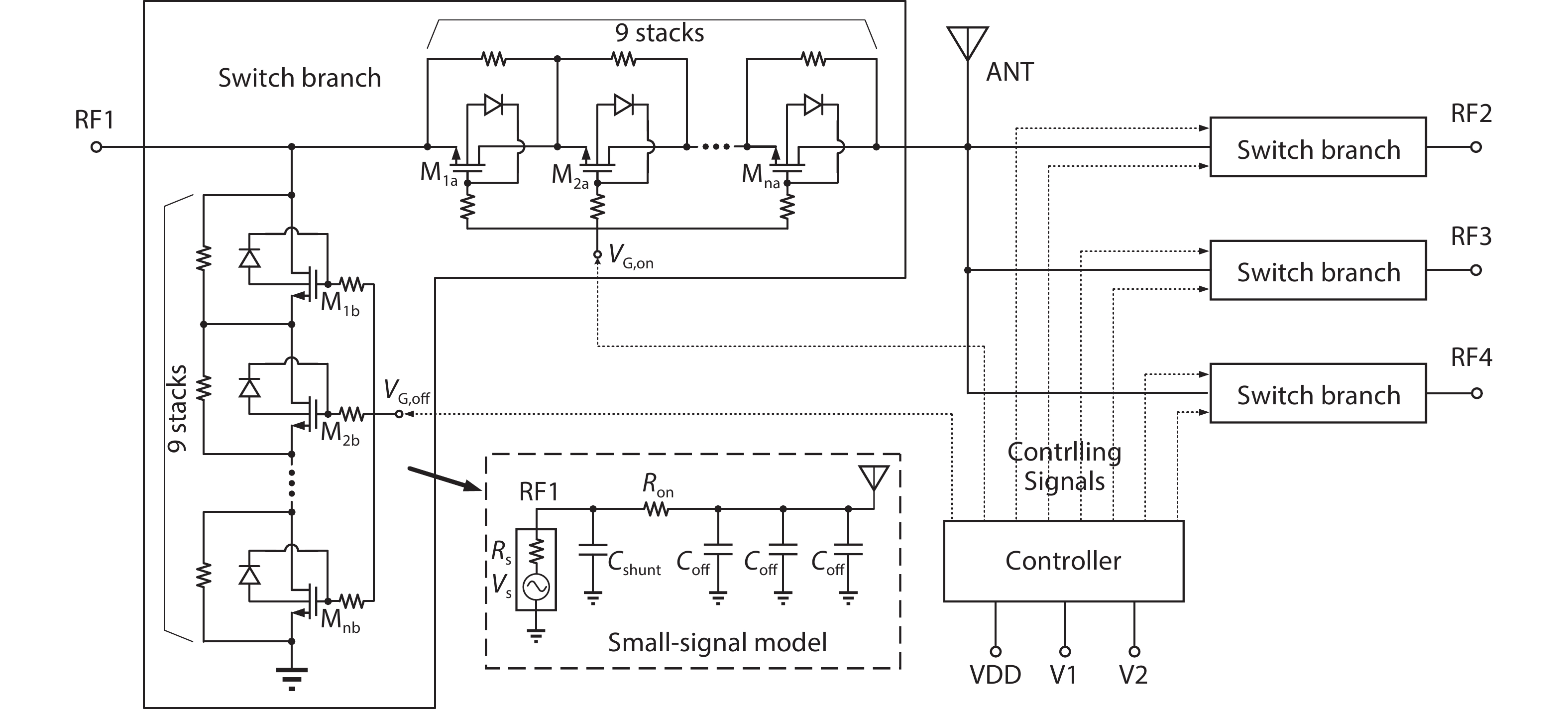
Fig. 1.  The block diagram of the proposed SP4T switch. Schematic of a single switch branch is depicted.

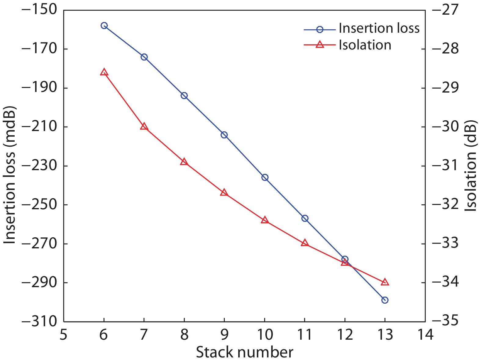
Fig. 2.  (Color online) IL and isolation at 1.98 GHz vs stack number.

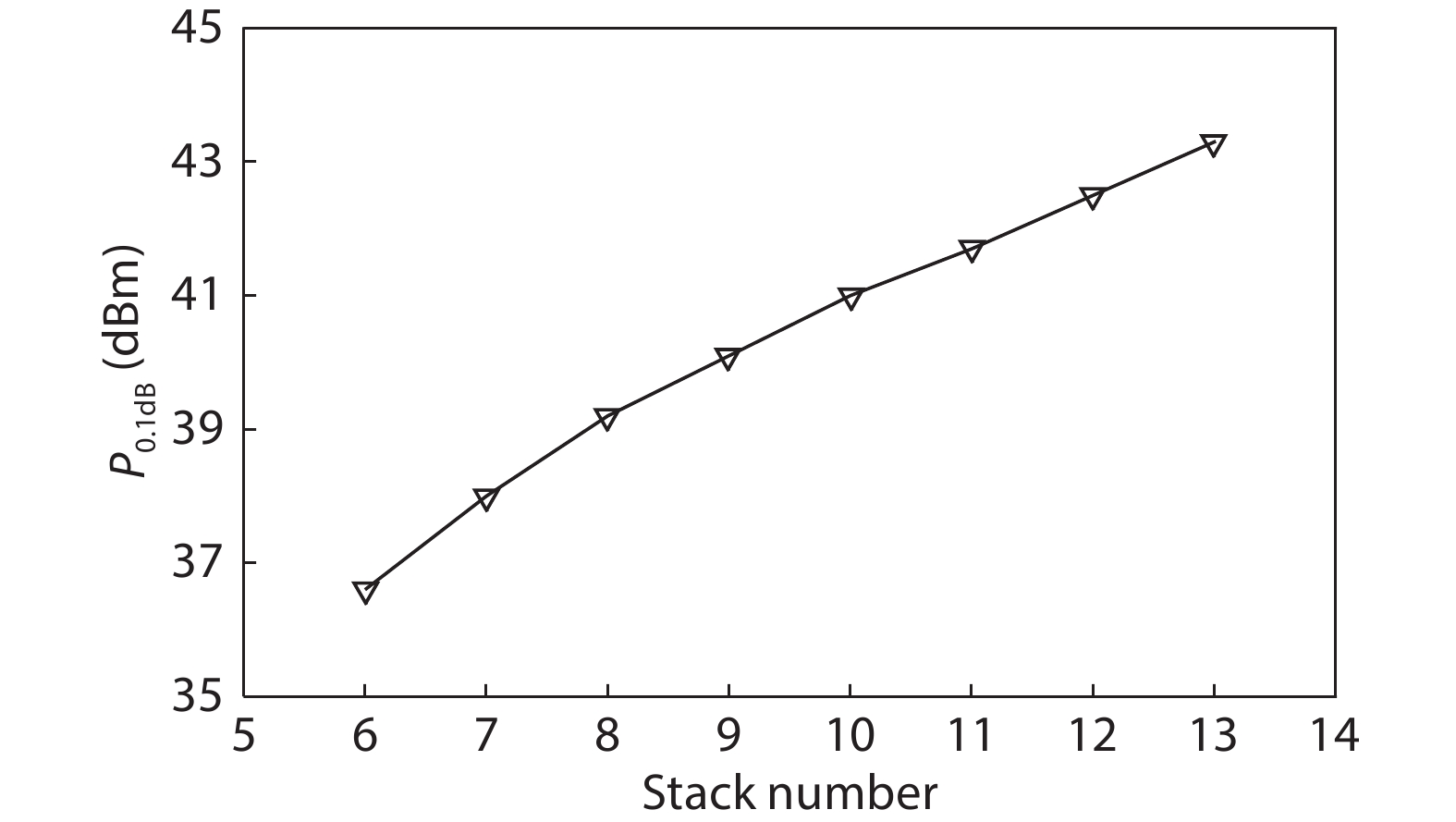
Fig. 3.  Input 0.1-dB compression point at 1.9 GHz vs. stack number.

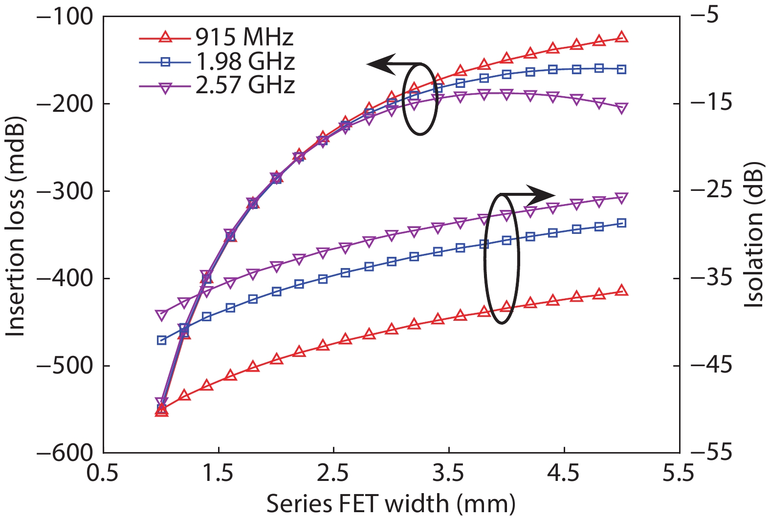
Fig. 4.  (Color online) IL and isolation vs series-FET width.

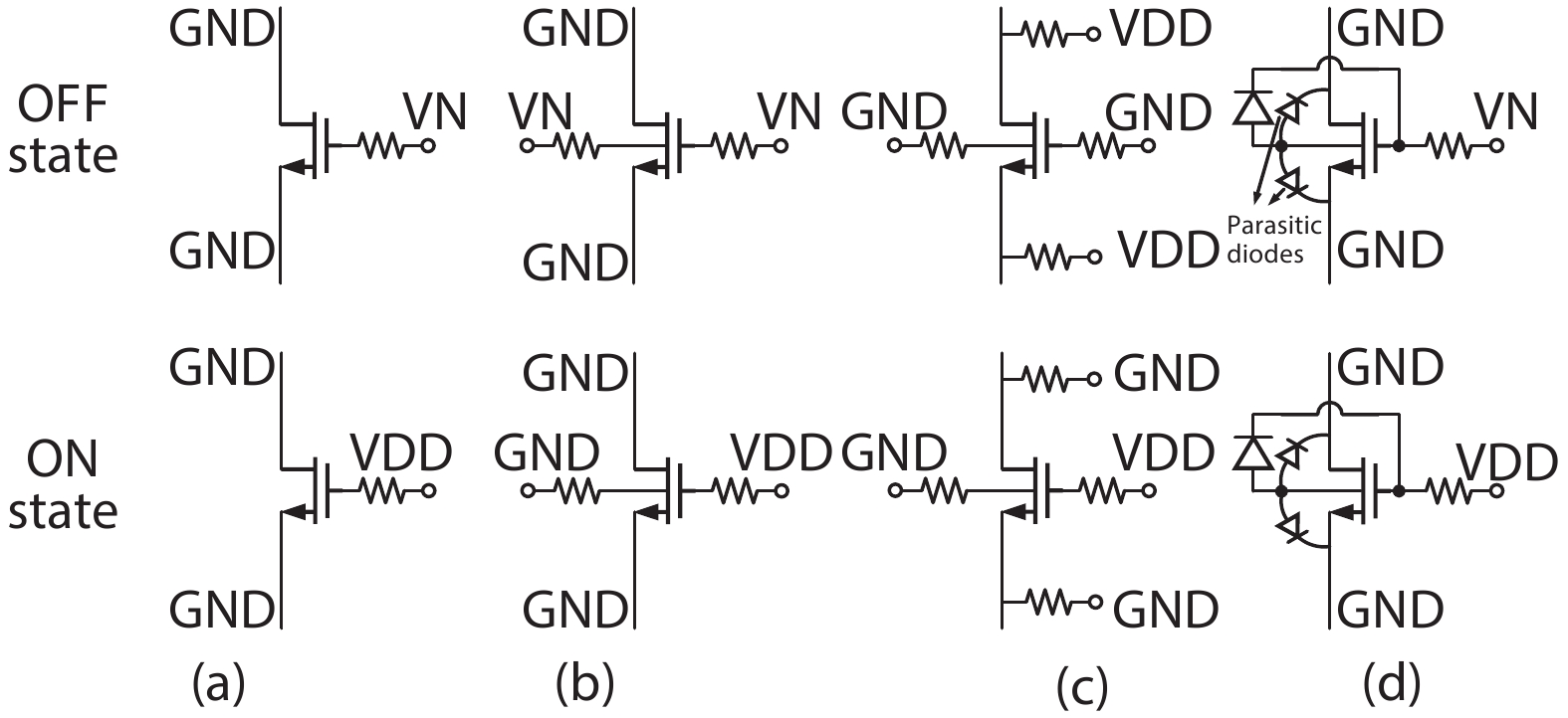
Fig. 5.  Different biasing strategies. (a) Floating body FET biasing. (b) Resistive body-floating biasing. (c) DC-lifting biasing. (d) Proposed body self-biasing strategy using diodes.

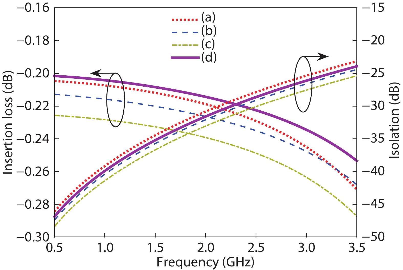
Fig. 6.  (Color online) IL and isolation of different biasing strategies.

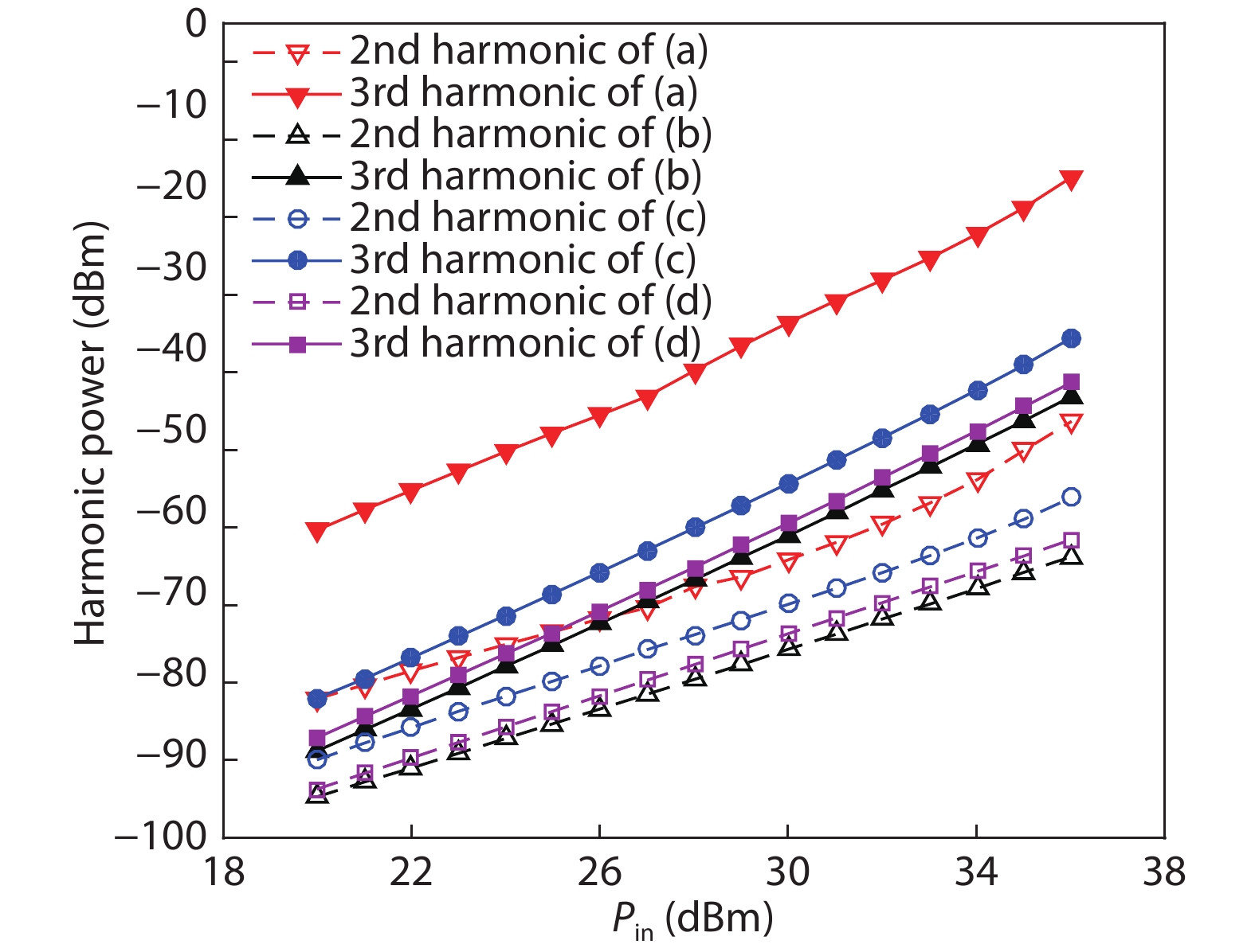
Fig. 7.  (Color online) Harmonic level at 1.98 GHz of different biasing strategies.

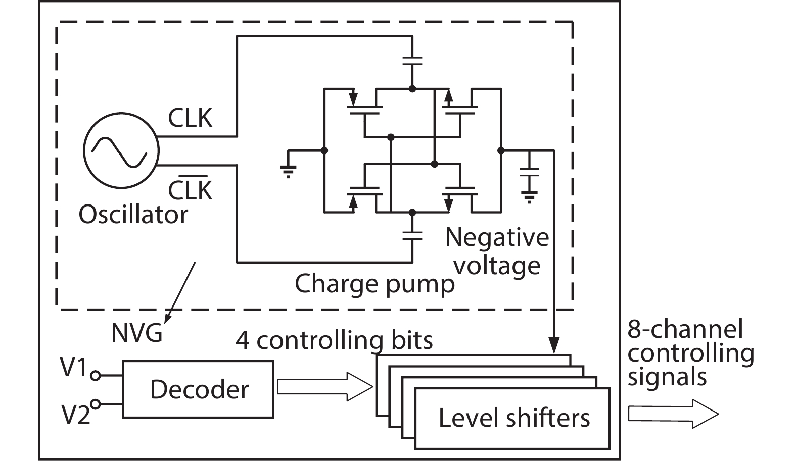
Fig. 8.  Block diagram of the controller.

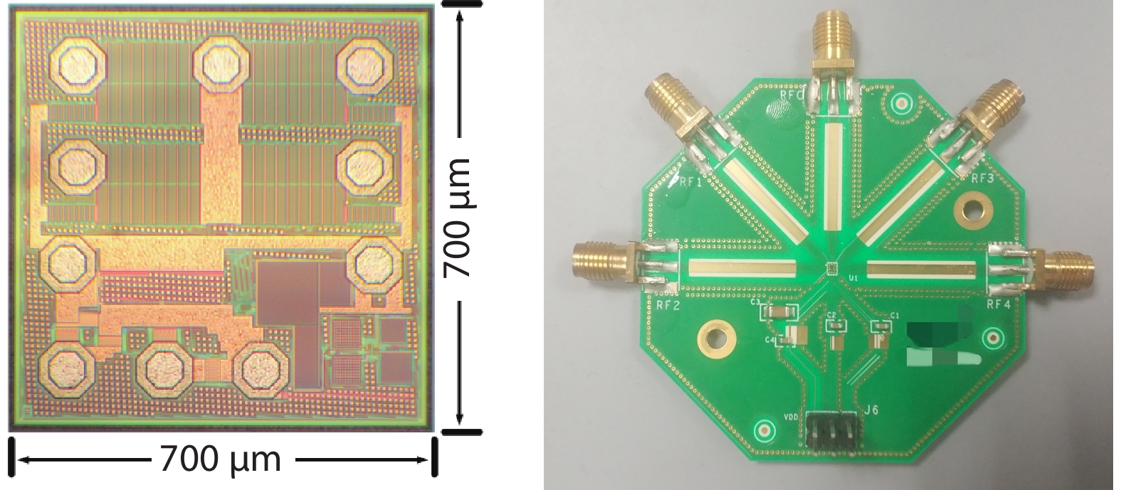
Fig. 9.  (Color online) Micrographs of the fabricated chip and evaluation board.

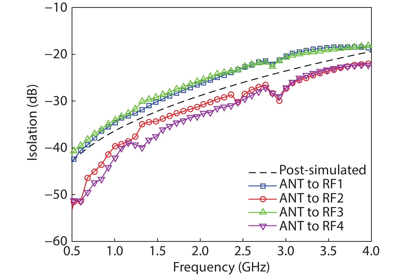
Fig. 11.  (Color online) Measured isolation of the proposed SP4T switch.

Fig. 12.  Simulated input power compression point of the SP4T switch.

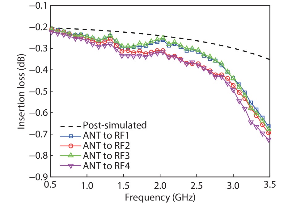
Fig. 10.  (Color online) Measured insertion loss of the SP4T switch.

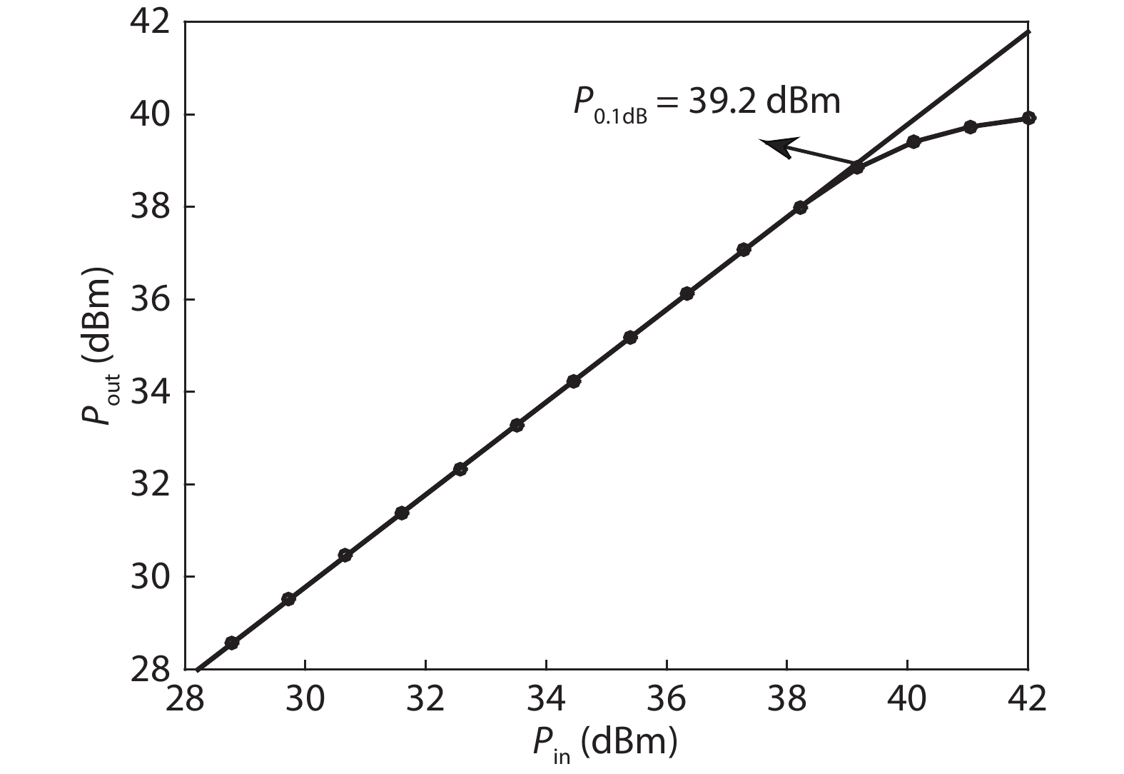
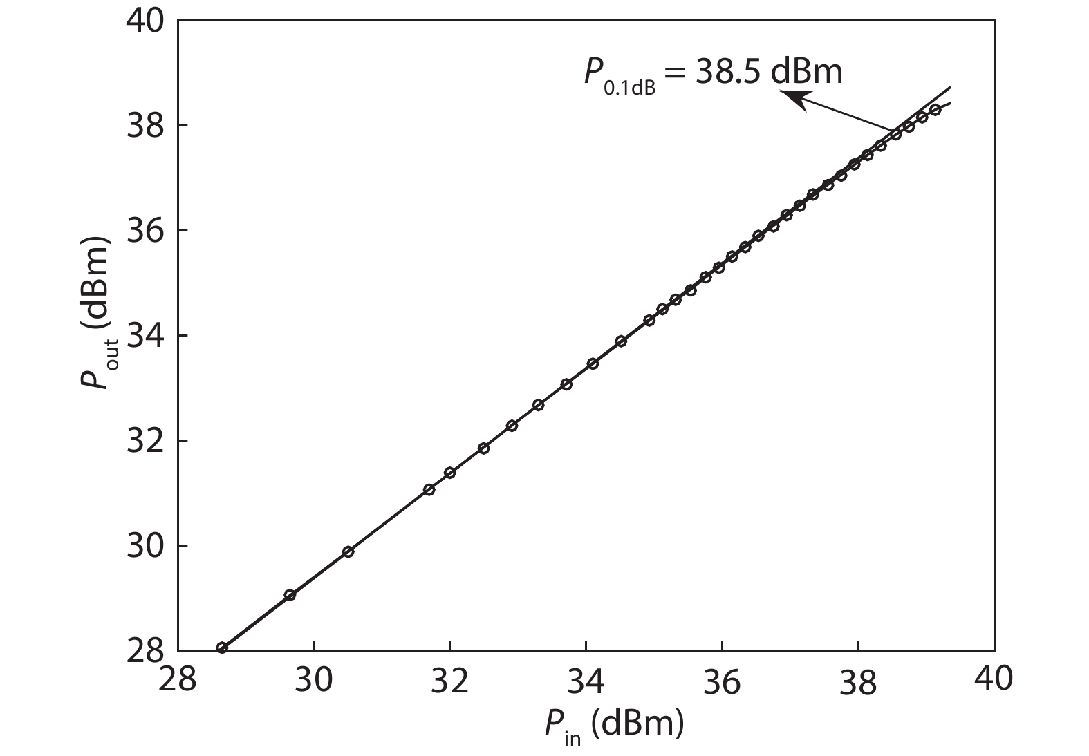
Fig. 13.  Measured input power compression point of the SP4T switch.

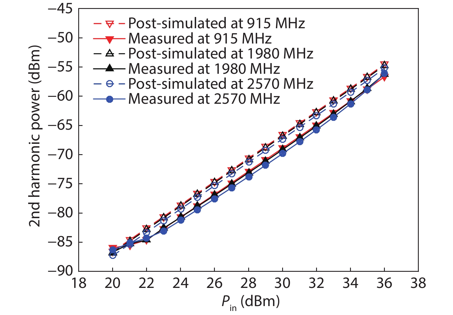
Fig. 14.  (Color online) Measured 2nd harmonics of the SP4T switch.

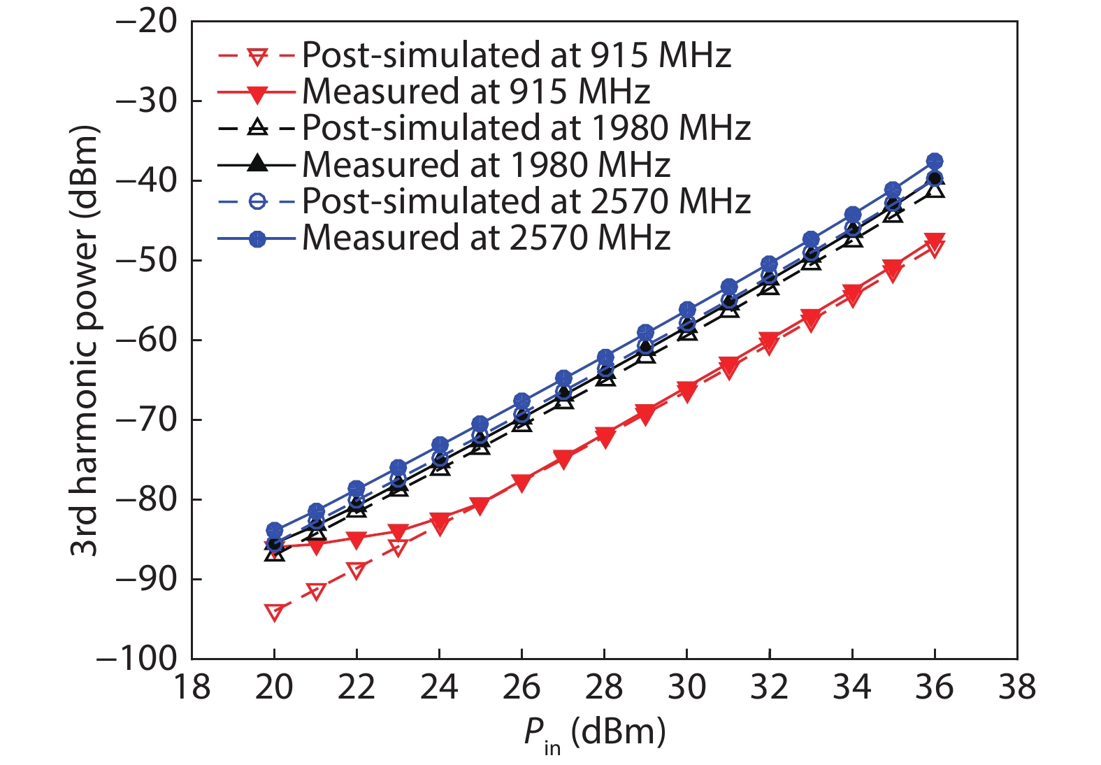
Fig. 15.  (Color online) Measured 3rd harmonics of the SP4T switch.

Table 1.   P0.1 dB at 1.9 GHz of different biasing strategies.

Biasing(a)(b)(c)(d)
P0.1 dB (dBm)37.340.236.740.1
DownLoad: CSV

Table 2.   Comparison of RF switch performance.

ParameterRef. [5]Ref. [6]Ref. [20]Ref. [21]This work
SPXTSP4TSP4TSPDTSPSTSP4T
f (GHz)0.90/1.90.90/1.90.90/1.90.90/1.90.90/1.9
Insertion loss (dB)0.49/0.700.30/0.370.25/0.300.24/0.340.27/0.33
Isolation (dB)37/3240/3329/2229/2235/27
P0.1 dB (dBm)38*NA35*3638.5
2nd Harmonic (dBc)**82/8390/8391/NA96****91/96
3rd Harmonic (dBc)**80/8185/7888/NA78****82/83
Area (mm2)0.98***1.01***0.430.200.49***
Stack number10NA10109
Biasing strategyImproved dc-liftingRBFTRBFTpFET body self-biasingDiode body self-biasing
Technology0.25 μm SOI CMOS0.13 μm SOI CMOS0.13 μm SOI CMOS0.13 μm SOI CMOS0.13 μm SOI CMOS
* 1-dB compression point. **Pin = 35 dBm at 900 MHz and 33 dBm at 1.9 GHz. *** including controller. **** frequency not specified.
DownLoad: CSV
[1]
Yan X, Li Y, Chen Y, et al. A LNA-merged RF front-end with digitally assisted technique for gain flatness and input-match compensation. Analog Integr Circuits Signal Process, 2019, 101, 219 doi: 10.1007/s10470-019-01539-2
[2]
Zhang H, Yan X, Shi J H, et al. A 0.5–5.6 GHz inductorless wideband LNA with local active feedback. 2018 IEEE 3rd International Conference on Integrated Circuits and Microsystems (ICICM), 2018, 164
[3]
Yan X, Chen C, Yang L, et al. A 0.1–1.1 GHz inductorless differential LNA with double gm -boosting and positive feedback. Analog Integr Circuits Signal Process, 2017, 93, 205 doi: 10.1007/s10470-017-1043-y
[4]
Huang C W P, Christainsen K, Nabokin S, et al. A highly integrated single chip 5–6 GHz front-end IC based on SiGe BiCMOS that enhances 802.11ac WLAN radio front-end designs. 2015 IEEE Radio Freq Integr Circuits Symp RFIC, 2015, 227
[5]
Im D, Kim B K, Im D K, et al. A stacked-FET linear SOI CMOS cellular antenna switch with an extremely low-power biasing strategy. IEEE Trans Microw Theory Tech, 2015, 63, 1964 doi: 10.1109/TMTT.2015.2427801
[6]
Ahn M, Cha J, Cho C, et al. Ultra low loss and high linearity SPMT antenna switch using SOI CMOS process. 40th Eur Microw Conf, 2010, 652
[7]
Joshi A B, Lee S, Chen Y Y, et al. Optimized CMOS-SOI process for high performance RF switches. 2012 IEEE Int SOI Conf SOI, 2012, 1
[8]
Ben Ali K, Roda Neve C, Gharsallah A, et al. Ultrawide frequency range crosstalk into standard and trap-rich high resistivity silicon substrates. IEEE Trans Electron Devices, 2011, 58, 4258 doi: 10.1109/TED.2011.2170074
[9]
Wang X S, Yue C P. A dual-band SP6T t/r switch in SOI CMOS with 37-dBm P–0.1 dB for GSM/W-CDMA handsets. IEEE Trans Theory Technol, 2014, 62, 861 doi: 10.1109/TMTT.2014.2308306
[10]
Ohnakado T, Yamakawa S, Murakami T, et al. 21.5 dBm power-handling 5 GHz transmit/receive CMOS switch realized by voltage division effect of stacked transistor configuration with depletion-layer-extended transistors (DETs). 2003 Symp VLSI Circuits Dig Tech Pap, 2003, 1152, 25
[11]
Ahn M, Lee C H, Kim B S, et al. A high-power CMOS switch using A novel adaptive voltage swing distribution method in multistack FETs. IEEE Trans Microw Theory Tech, 2008, 56, 849 doi: 10.1109/TMTT.2008.919047
[12]
Ahn M, Kim H W, Lee C H, et al. A 1.8-GHz 33-dBm P0.1-dB CMOS T/R switch using stacked FETs with feed-forward capacitors in a floated well structure. IEEE Trans Microw Theory Tech, 2009, 57, 2661 doi: 10.1109/TMTT.2009.2031928
[13]
Cui J, Chen L, Liu Y. Monolithic single-pole sixteen-throw T/R switch for next-generation front-end module. IEEE Microw Wirel Compon Lett, 2014, 24, 345 doi: 10.1109/LMWC.2014.2309082
[14]
Yeh M C, Tsai Z M, Liu R C, et al. Design and analysis for a miniature CMOS SPDT switch using body-floating technique to improve power performance. IEEE Trans Microw Theory Tech, 2006, 54, 31 doi: 10.1109/TMTT.2005.860894
[15]
Tinella C, Richard O, Cathelin A, et al. 0.13 μm CMOS SOI SP6T antenna switch for multi-standard handsets. 2006 Topical Meeting on Silicon Monolithic Integrated Circuits in RF Systems, 2006, 4
[16]
Zhang Z H, Huang L, Yu K, et al. A novel body self-biased technique for enhanced RF performance of a SP8T antenna switch in partially depleted CMOS-SOI technology. 2014 12th IEEE International Conference on Solid-State and Integrated Circuit Technology (ICSICT), 2014, 1
[17]
Xu H F, Kenneth K O. A 31.3-dBm bulk CMOS T/R switch using stacked transistors with sub-design-rule channel length in floated p-wells. IEEE J Solid-State Circuits, 2007, 42, 2528 doi: 10.1109/JSSC.2007.907201
[18]
Tseng Y C, Huang W M, Monk D J, et al. AC floating body effects and the resultant analog circuit issues in submicron floating body and body-grounded SOI MOSFET's. IEEE Trans Electron Devices, 1999, 46, 1685 doi: 10.1109/16.777157
[19]
Cha J, Ahn M, Cho C, et al. Analysis and design techniques of CMOS charge-pump-based radio-frequency antenna-switch controllers. IEEE Trans Circuits Syst I, 2009, 56, 1053 doi: 10.1109/TCSI.2009.2016129
[20]
Zhu H W, Li Q L, Sun H, et al. Ultra low loss and high linearity RF switch using 130 nm SOI CMOS process. 2017 IEEE 12th International Conference on ASIC (ASICON), 2017, 698
[21]
Guan H, Sun H, Bao J L, et al. High-performance RF switch in 0.13 μm RF SOI process. J Semicond, 2019, 40, 022401 doi: 10.1088/1674-4926/40/2/022401
  • Search

    Advanced Search >>

    GET CITATION

    shu

    Export: BibTex EndNote

    Article Metrics

    Article views: 4406 Times PDF downloads: 111 Times Cited by: 0 Times

    History

    Received: 21 January 2020 Revised: 20 April 2020 Online: Accepted Manuscript: 23 June 2020Uncorrected proof: 28 June 2020Published: 01 October 2020

    Catalog

      Email This Article

      User name:
      Email:*请输入正确邮箱
      Code:*验证码错误
      Hao Zhang, Qiangsheng Cui, Xu Yan, Jiahui Shi, Fujiang Lin. A 0.5–3.0 GHz SP4T RF switch with improved body self-biasing technique in 130-nm SOI CMOS[J]. Journal of Semiconductors, 2020, 41(10): 102404. doi: 10.1088/1674-4926/41/10/102404 ****Hao Zhang, Qiangsheng Cui, Xu Yan, Jiahui Shi, Fujiang Lin. 2020: A 0.5–3.0 GHz SP4T RF switch with improved body self-biasing technique in 130-nm SOI CMOS. Journal of Semiconductors, 41(10): 102404. doi: 10.1088/1674-4926/41/10/102404
      Citation:
      Hao Zhang, Qiangsheng Cui, Xu Yan, Jiahui Shi, Fujiang Lin. A 0.5–3.0 GHz SP4T RF switch with improved body self-biasing technique in 130-nm SOI CMOS[J]. Journal of Semiconductors, 2020, 41(10): 102404. doi: 10.1088/1674-4926/41/10/102404 ****
      Hao Zhang, Qiangsheng Cui, Xu Yan, Jiahui Shi, Fujiang Lin. 2020: A 0.5–3.0 GHz SP4T RF switch with improved body self-biasing technique in 130-nm SOI CMOS. Journal of Semiconductors, 41(10): 102404. doi: 10.1088/1674-4926/41/10/102404

      A 0.5–3.0 GHz SP4T RF switch with improved body self-biasing technique in 130-nm SOI CMOS

      doi: 10.1088/1674-4926/41/10/102404
      More Information
      • Corresponding author: F J Lin, linfj@ustc.edu.cn
      • Received Date: 2020-01-21
      • Revised Date: 2020-04-20
      • Available Online: 2022-07-22

      Catalog

        /

        DownLoad:  Full-Size Img  PowerPoint
        Return
        Return