J. Semicond. > 2020, Volume 41 > Issue 12 > 122103

ARTICLES

The etching process and mechanism analysis of Ta-Sb2Te3 film based on inductively coupled plasma

Yongkang Xu1, 2, Sannian Song1, , Wencheng Fang1, 2, Chengxing Li1, 2 and Zhitang Song1

+ Author Affiliations

 Corresponding author: Sannian Song, songsannian@mail.sim.ac.cn

DOI: 10.1088/1674-4926/41/12/122103

PDF

Turn off MathJax

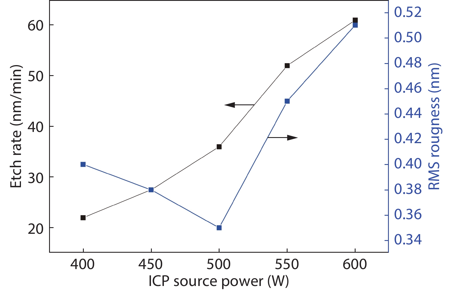
Abstract: Compared to the conventional phase change materials, the new phase change material Ta-Sb2Te3 has the advantages of excellent data retention and good material stability. In this letter, the etching characteristics of Ta-Sb2Te3 were studied by using CF4/Ar. The results showed that when CF4/Ar = 25/25, the etching power was 600 W and the etching pressure was 2.5 Pa, the etching speed was up to 61 nm/min. The etching pattern of Ta-Sb2Te3 film had a smooth side wall and good perpendicularity (close to 90°), smooth surface of the etching (RMS was 0.51nm), and the etching uniformity was fine. Furthermore, the mechanism of this etching process was analyzed by X-ray photoelectron spectroscopy (XPS). The main damage mechanism of ICP etching in CF4/Ar was studied by X-ray diffraction (XRD).

Key words: new phase change materialinductively couple plasmaetching processetching characteristicsmechanism


[1]
Ovshinsky S R. Reversible electrical switching phenomena in disordered structures. Phys Rev Lett, 1968, 21, 1450 doi: 10.1103/PhysRevLett.21.1450
[2]
Washington J S, Joseph E A, Raoux S, et al. Characterizing the effects of etch-induced material modification on the crystallization properties of nitrogen doped Ge2Sb2Te5. J Appl Phys, 2011, 109, 034502 doi: 10.1063/1.3524510
[3]
Xu C, Liu B, Song Z T, et al. Reactive-ion etching of Sn-doped Ge2Sb2Te5 in CHF3/O2 plasma for non-volatile phase-change memory device. Thin Solid Films, 2008, 516, 7871 doi: 10.1016/j.tsf.2008.05.039
[4]
Song Z T, Song S N, Zhu M, et al. From octahedral structure motif to sub-nanosecond phase transitions in phase change materials for data storage. Sci China Inf Sci, 2018, 61, 081302 doi: 10.1007/s11432-018-9404-2
[5]
Rao F, Song Z T, Ren K, et al. Si–Sb–Te materials for phase change memory applications. Nanotechnology, 2011, 22, 145702 doi: 10.1088/0957-4484/22/14/145702
[6]
Li J T, Xia Y Y, Liu B, et al. Direct evidence of reactive ion etching induced damages in Ge2Sb2Te5 based on different halogen plasmas. Appl Surf Sci, 2016, 378, 163 doi: 10.1016/j.apsusc.2016.03.122
[7]
Li J T, Xia Y Y, Liu B, et al. Etch characteristics and mechanism of TiSbTe thin films in inductively-coupled HBr-He, Ar, N2, O2 plasma. ECS J Solid State Sci Technol, 2016, 5, P330 doi: 10.1149/2.0201606jss
[8]
Shen L L, Song S N, Zhang Z H, et al. Characteristics and mechanism of phase change material W0.03Sb2Te etched by Cl2/BCl3 inductively coupled plasmas. Thin Solid Films, 2015, 593, 67 doi: 10.1016/j.tsf.2015.09.032
[9]
Zhang Z H, Song S N, Song Z T, et al. Characteristics and mechanism of Al1.3Sb3Te etched by Cl2/BCl3 inductively coupled plasmas. Microelectron Eng, 2014, 115, 51 doi: 10.1016/j.mee.2013.10.016
[10]
Kang S K, Jeon M H, Park J Y, et al. Etch damage of Ge2Sb2Te5 for different halogen gases. Jpn J Appl Phys, 2011, 50, 086501 doi: 10.1143/JJAP.50.086501
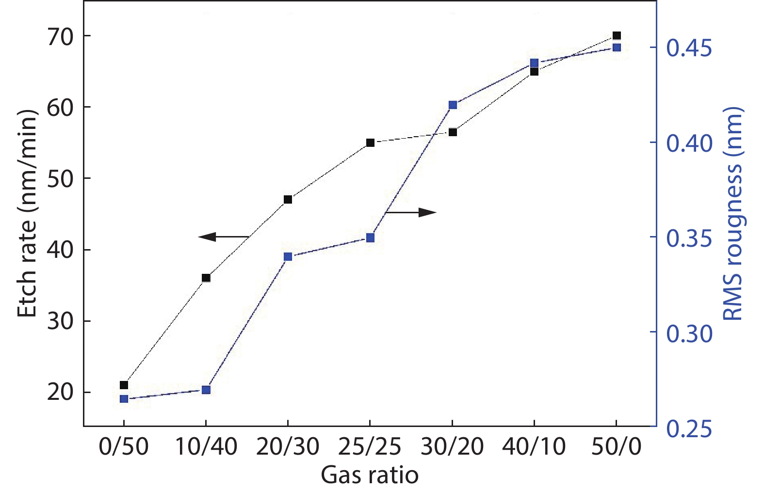
Fig. 1.  Effect of gas composition on etching rate and surface roughness.

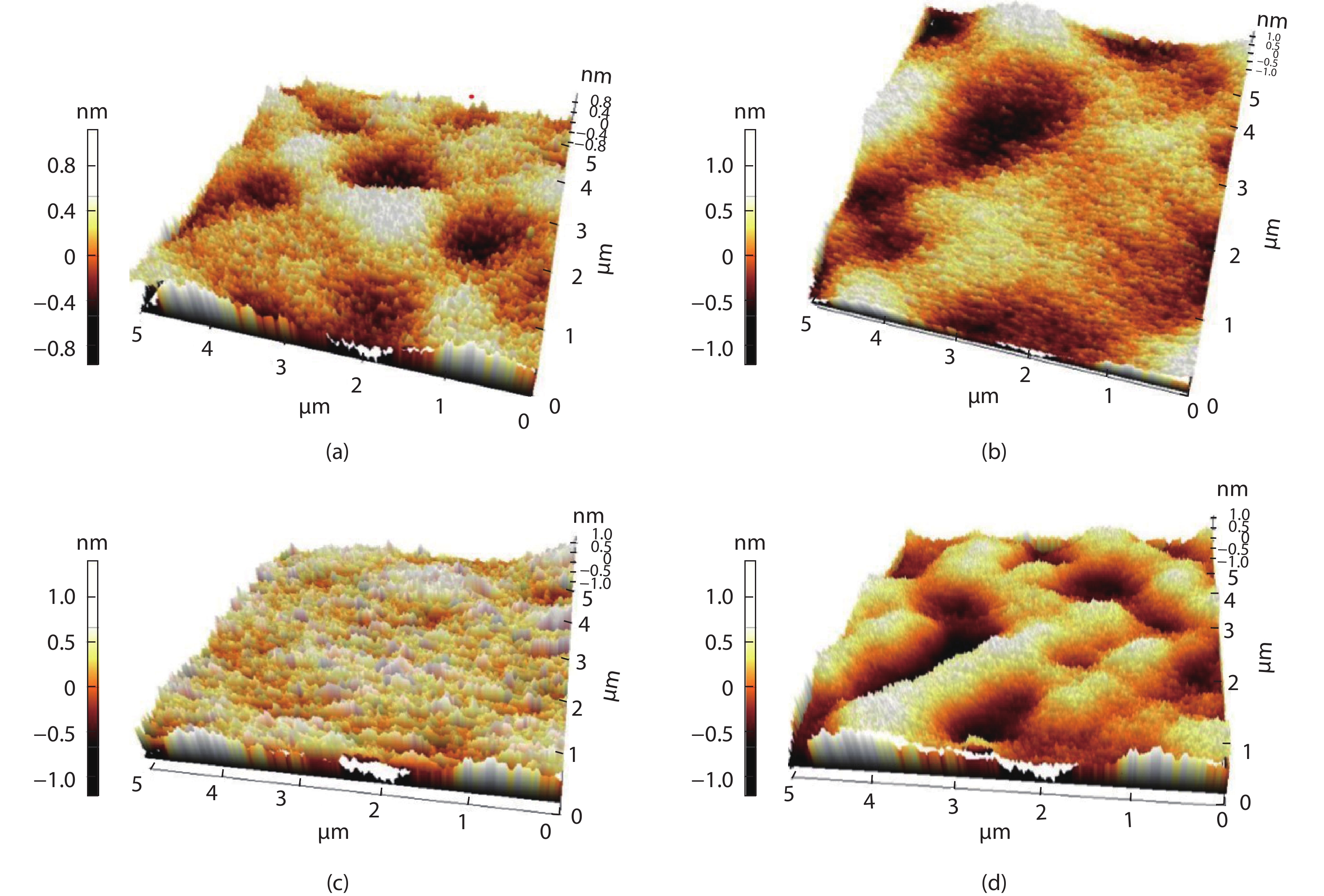
Fig. 2.  (Color online) AFM images of Ta-Sb2Te3 surface (a) CF4/Ar = 10/40, RMS = 0.27, (b) CF4/Ar = 20/30, RMS = 0.34, (c) CF4/Ar = 25/25, RMS = 0.35, (d) CF4/Ar = 30/20 and RMS = 0.42.

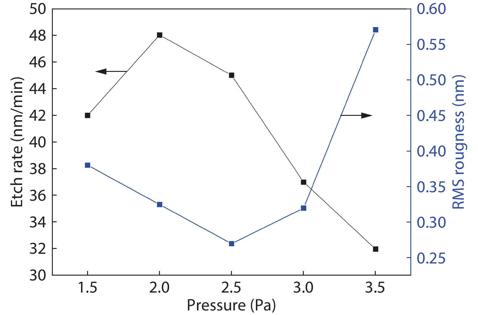
Fig. 3.  Effect of chamber pressure on etching rate and surface roughness.

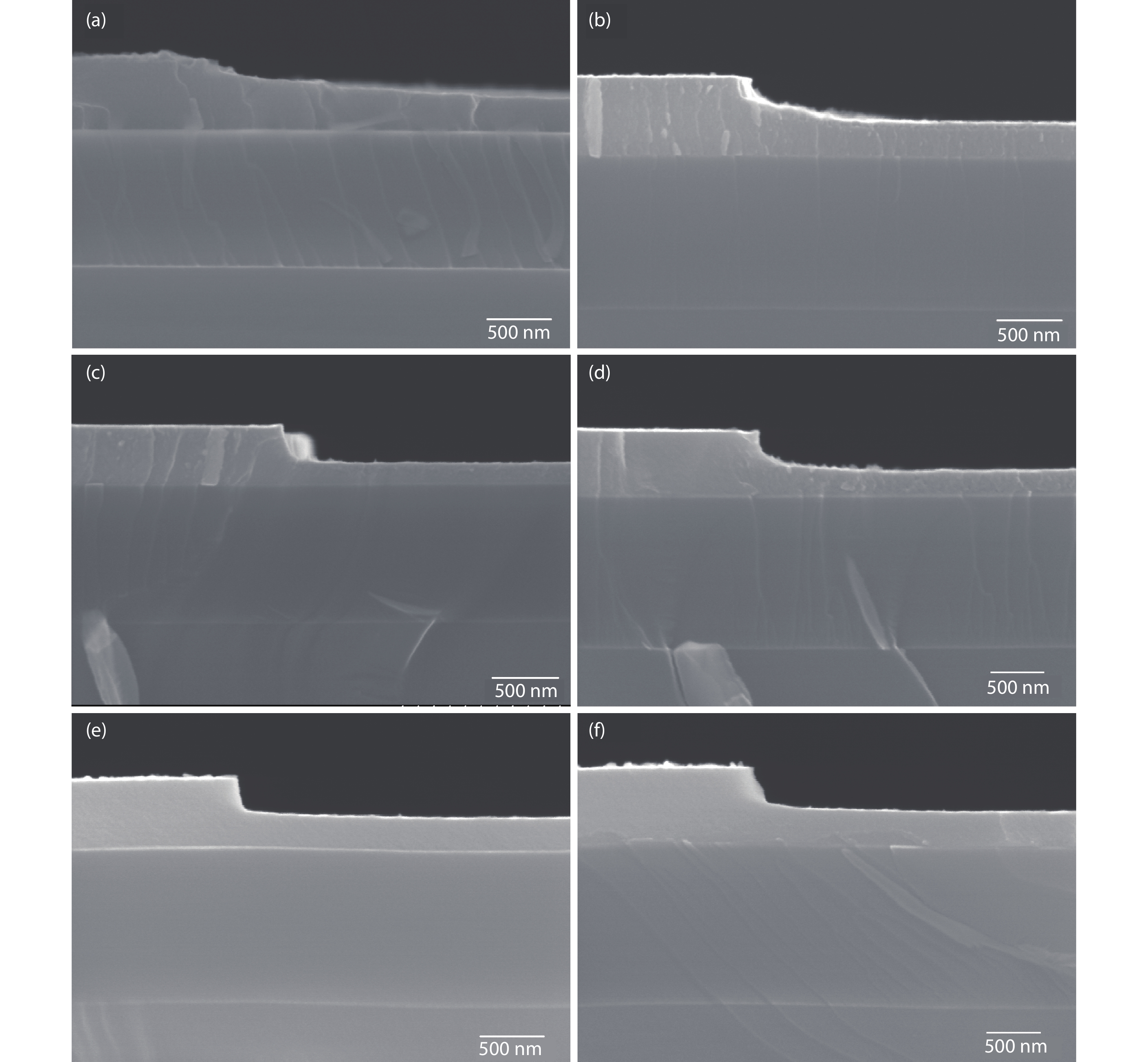
Fig. 4.  SEM of cross sections of Ta-Sb2Te3 after ICP etching with pressure of (a)1.0 Pa, (b) 1.5 Pa, (c) 2.0 Pa, (d) 2.25 Pa, (e) 2.5 Pa, (f) 2.75 Pa with CF4 flow of 25 sccm, Ar flow of 25 sccm, ICP power of 600 W.

Fig. 5.  Effects of ICP source power on RMS roughness and etching rate of Ta-Sb2Te3.

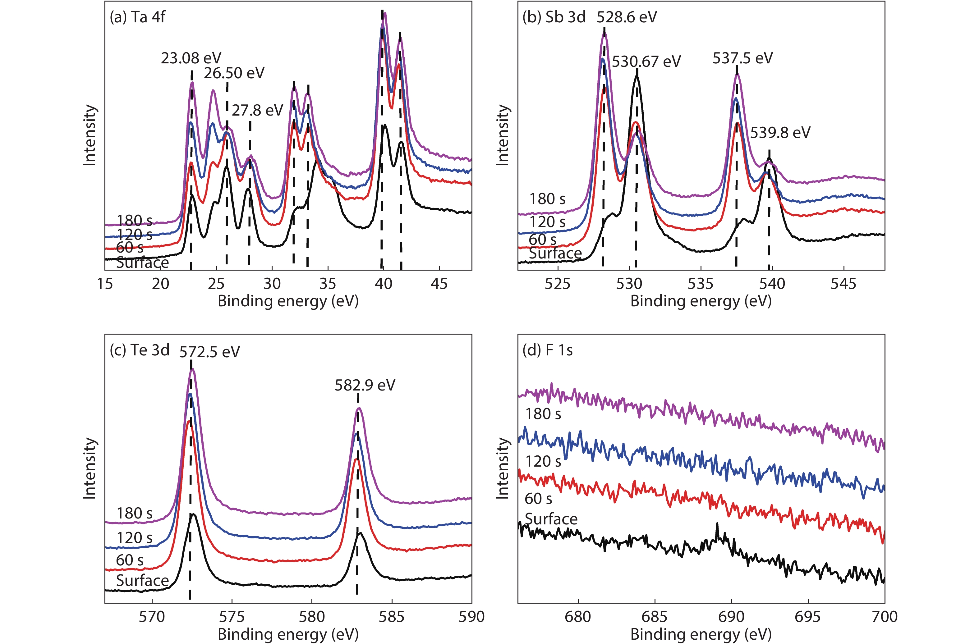
Fig. 6.  (Color online) XPS spectrum of each component of the Ta-Sb2Te3 film after ICP etching.

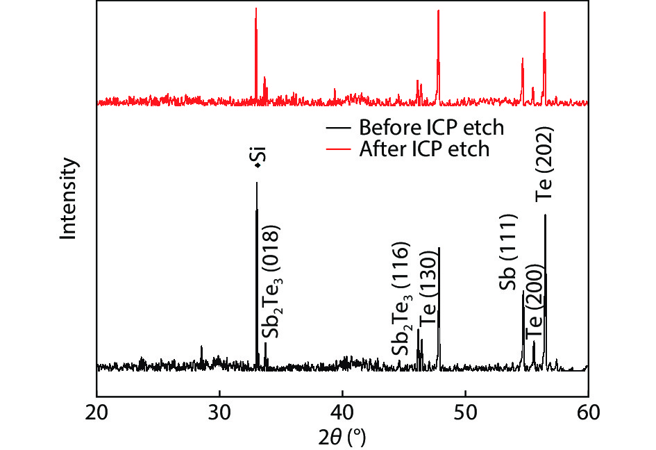
Fig. 7.  (Color online) XRD curves before and after ICP etching.

Table 1.   The boiling point of fluoride.

ElementChemical compoundBoiling point (°C)
SbSbF5141
SbSbF3345
TeTeF4195
TeTeF6–39
DownLoad: CSV
[1]
Ovshinsky S R. Reversible electrical switching phenomena in disordered structures. Phys Rev Lett, 1968, 21, 1450 doi: 10.1103/PhysRevLett.21.1450
[2]
Washington J S, Joseph E A, Raoux S, et al. Characterizing the effects of etch-induced material modification on the crystallization properties of nitrogen doped Ge2Sb2Te5. J Appl Phys, 2011, 109, 034502 doi: 10.1063/1.3524510
[3]
Xu C, Liu B, Song Z T, et al. Reactive-ion etching of Sn-doped Ge2Sb2Te5 in CHF3/O2 plasma for non-volatile phase-change memory device. Thin Solid Films, 2008, 516, 7871 doi: 10.1016/j.tsf.2008.05.039
[4]
Song Z T, Song S N, Zhu M, et al. From octahedral structure motif to sub-nanosecond phase transitions in phase change materials for data storage. Sci China Inf Sci, 2018, 61, 081302 doi: 10.1007/s11432-018-9404-2
[5]
Rao F, Song Z T, Ren K, et al. Si–Sb–Te materials for phase change memory applications. Nanotechnology, 2011, 22, 145702 doi: 10.1088/0957-4484/22/14/145702
[6]
Li J T, Xia Y Y, Liu B, et al. Direct evidence of reactive ion etching induced damages in Ge2Sb2Te5 based on different halogen plasmas. Appl Surf Sci, 2016, 378, 163 doi: 10.1016/j.apsusc.2016.03.122
[7]
Li J T, Xia Y Y, Liu B, et al. Etch characteristics and mechanism of TiSbTe thin films in inductively-coupled HBr-He, Ar, N2, O2 plasma. ECS J Solid State Sci Technol, 2016, 5, P330 doi: 10.1149/2.0201606jss
[8]
Shen L L, Song S N, Zhang Z H, et al. Characteristics and mechanism of phase change material W0.03Sb2Te etched by Cl2/BCl3 inductively coupled plasmas. Thin Solid Films, 2015, 593, 67 doi: 10.1016/j.tsf.2015.09.032
[9]
Zhang Z H, Song S N, Song Z T, et al. Characteristics and mechanism of Al1.3Sb3Te etched by Cl2/BCl3 inductively coupled plasmas. Microelectron Eng, 2014, 115, 51 doi: 10.1016/j.mee.2013.10.016
[10]
Kang S K, Jeon M H, Park J Y, et al. Etch damage of Ge2Sb2Te5 for different halogen gases. Jpn J Appl Phys, 2011, 50, 086501 doi: 10.1143/JJAP.50.086501
  • Search

    Advanced Search >>

    GET CITATION

    shu

    Export: BibTex EndNote

    Article Metrics

    Article views: 3508 Times PDF downloads: 55 Times Cited by: 0 Times

    History

    Received: 22 April 2020 Revised: 26 May 2020 Online: Accepted Manuscript: 11 August 2020Uncorrected proof: 19 August 2020Published: 08 December 2020

    Catalog

      Email This Article

      User name:
      Email:*请输入正确邮箱
      Code:*验证码错误
      Yongkang Xu, Sannian Song, Wencheng Fang, Chengxing Li, Zhitang Song. The etching process and mechanism analysis of Ta-Sb2Te3 film based on inductively coupled plasma[J]. Journal of Semiconductors, 2020, 41(12): 122103. doi: 10.1088/1674-4926/41/12/122103 ****Y K Xu, S N Song, W C Fang, C X Li, Z T Song, The etching process and mechanism analysis of Ta-Sb2Te3 film based on inductively coupled plasma[J]. J. Semicond., 2020, 41(12): 122103. doi: 10.1088/1674-4926/41/12/122103.
      Citation:
      Yongkang Xu, Sannian Song, Wencheng Fang, Chengxing Li, Zhitang Song. The etching process and mechanism analysis of Ta-Sb2Te3 film based on inductively coupled plasma[J]. Journal of Semiconductors, 2020, 41(12): 122103. doi: 10.1088/1674-4926/41/12/122103 ****
      Y K Xu, S N Song, W C Fang, C X Li, Z T Song, The etching process and mechanism analysis of Ta-Sb2Te3 film based on inductively coupled plasma[J]. J. Semicond., 2020, 41(12): 122103. doi: 10.1088/1674-4926/41/12/122103.

      The etching process and mechanism analysis of Ta-Sb2Te3 film based on inductively coupled plasma

      DOI: 10.1088/1674-4926/41/12/122103
      More Information

      Catalog

        /

        DownLoad:  Full-Size Img  PowerPoint
        Return
        Return