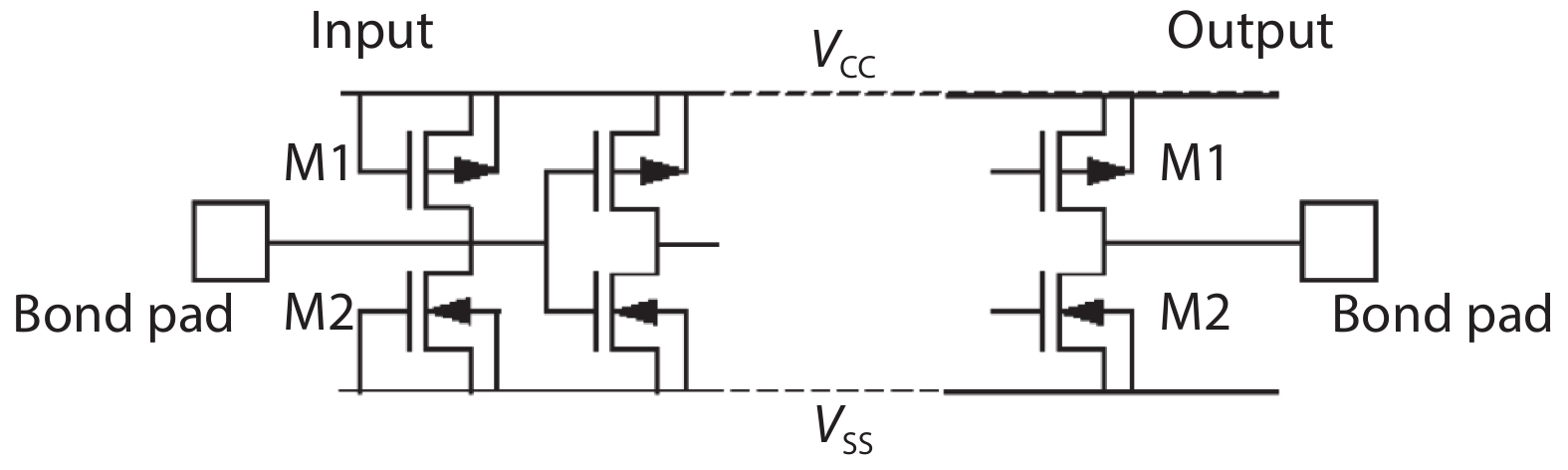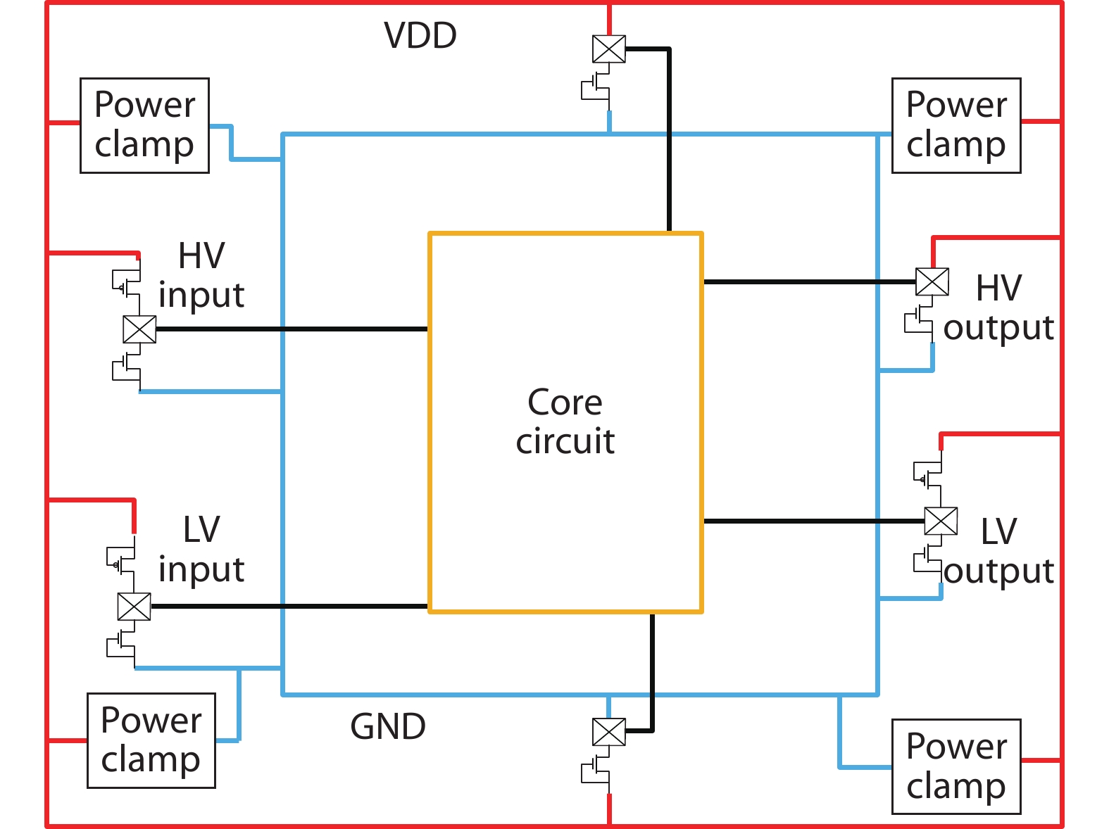
Fig. 1.
(Color online) The structure of IC (integrated circuit) chip ESD protection system.
ARTICLES
Jianwei Wu, Zongguang Yu, Genshen Hong and Rubin Xie
Corresponding author: Zongguang Yu, email: yuzg58@163.com
Abstract: In this paper, the ESD discharge capability of GGNMOS (gate grounded NMOS) device in the radiation-hardened 0.18 μm bulk silicon CMOS process (Rad-Hard by Process: RHBP) is optimized by layout and ion implantation design. The effects of gate length, DCGS and ESD ion implantation of GGNMOS on discharge current density and lattice temperature are studied by TCAD and device simulation. The size of DCGS, multi finger number and single finger width of ESD verification structures are designed, and the discharge capacity and efficiency of GGNMOS devices in ESD are characterized by TLP test technology. Finally, the optimized GGNMOS is verified on the DSP circuit, and its ESD performance is over 3500 V in HBM mode.
Keywords: total ionizing dose, RHBP, GGNMOS, ESD ion implantation, STI, TLP, leakage current, DCGS
| [1] |
Kepens B. On-chip ESD solutions seminar. SOFICS, Shanghai, 2015
|
| [2] |
Xie R B, Ji X M, Wu J W. Research on ESD performance of devices in radiation hardening process. Microprocessors, 2019, 40, 1 doi: 10.3969/j.issn.1002-2279.2019.03.001
|
| [3] |
Wang A Z H. On-chip ESD protection for integrated circuits: An IC design perspective. Springer Science & Business Media, 2006
|
| [4] |
Zhang L Z, Wang Y, Wang Y Z, et al. Insight into multiple-triggering effect in DTSCRs for ESD protection. J Semicond, 2017, 38, 075001 doi: 10.1088/1674-4926/38/7/075001
|
| [5] |
Bi X W, Liang H L, Gu X F, et al. Design of novel DDSCR with embedded PNP structure for ESD protection. J Semicond, 2015, 36, 124007 doi: 10.1088/1674-4926/36/12/124007
|
| [6] |
Mohan N, Kumar A. ESD protection design methodology in deep sub-micron CMOS technologies. Project Report, Course E&CE 730 (Topic 9), 2003, 5
|
| [7] |
Jiang Y X, Li J, Ran F, et al. Influence of layout parameters on snapback characteristic for a gate-grounded NMOS device in 0.13-μm silicide CMOS technology. J Semicond, 2009, 30, 084007 doi: 10.1088/1674-4926/30/8/084007
|
| [8] |
Chen T Y, Ker M D. Analysis on the dependence of layout parameters on ESD robustness of CMOS devices for manufacturing in deep-submicron CMOS process. IEEE Trans Semicond Manuf, 2003, 16, 486 doi: 10.1109/TSM.2003.815200
|
| [9] |
Do K I, Park J G, Kwon M J, et al. Analysis of GGNMOS-based ESD protection device using DCGS variation with robustness. Academic Conference of Korean Institute of Electronic Engineering, 2016, 6, 74
|
| [10] |
Krabbenborg B, Beltman R, Wolbert P, et al. Physics of electro-thermal effects in ESD protection devices. J Electrost, 1992, 28, 285 doi: 10.1016/0304-3886(92)90077-7
|
| [11] |
Chen J Z, Zhang X Y, Amerasekera A, et al. Design and layout of a high ESD performance NPN structure for submicron BiCMOS/bipolar circuits. Proceedings of International Reliability Physics Symposium, 1996
|
| [12] |
Ker M D, Chen T Y. Substrate-triggered technique for on-chip ESD protection design in a 0.18-μm salicided CMOS process. IEEE Trans Electron Devices, 2003, 50, 1050 doi: 10.1109/TED.2003.812495
|
| [13] |
Wu D X, Jiang L L, Fan H, et al. Analysis on the positive dependence of channel length on ESD failure current of a GGNMOS in a 5 V CMOS. J Semicond, 2013, 34, 024004 doi: 10.1088/1674-4926/34/2/024004
|
| [14] |
Wu J W, Yu Z G, Hong G S, et al. A method for strengthening the total ionizing dose of 0.18 μm bulk CMOS process. 2018 International Conference on Radiation Effects of Electronic Devices, 2018
|
| [15] |
Paul M, Russ C, Kumar B S, et al. Physics of current filamentation in ggNMOS devices under ESD condition revisited. IEEE Trans Electron Devices, 2018, 65, 2981 doi: 10.1109/TED.2018.2835831
|
| [16] |
Wang Y, Lu G Y, Wang Y Z, et al. Power-rail ESD clamp circuit with parasitic-BJT and channel parallel shunt paths to achieve enhanced robustness. IEICE Trans Electron, 2017, E100.C, 344 doi: 10.1587/transele.E100.C.344
|
| [17] |
Li L, Zhu K H. ESD performance analysis of gate grounded NMOS devices. Electron Pack, 2011, 11, 18 doi: 10.3969/j.issn.1681-1070.2011.02.006
|
| [18] |
Li Z G, Yue S G, Sun Y Z. Research on ESD device design of deep submicron IC. The 16th National Conference on Silicon Materials for Semiconductor Integrated circuits, 2009
|
| [19] |
Li Z G, Yue S G, Sun Y S. GDNMOS design for ESD protection in submicron CMOS VLSI. 2009 Asia Pacific Conference on Postgraduate Research in Microelectronics & Electronics, 2009, 432
|
| [20] |
Shi J. Deep sub-micron ESD GGNMOS layout design and optimization. MATEC Web Conf, 2018, 198, 04009 doi: 10.1051/matecconf/201819804009
|
| [21] |
Boschke R, Chen S H, Scholz M, et al. ESD ballasting of Ge FinFET ggNMOS devices. 2017 IEEE International Reliability Physics Symposium (IRPS) – Monterey, 2017
|
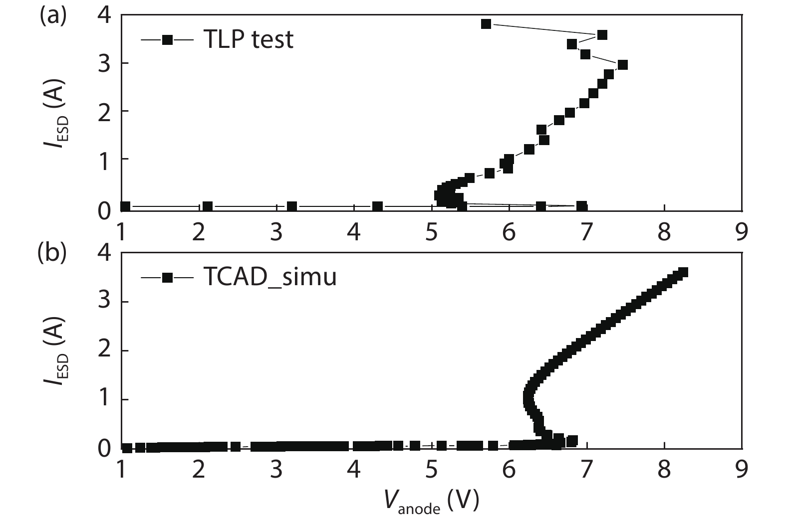
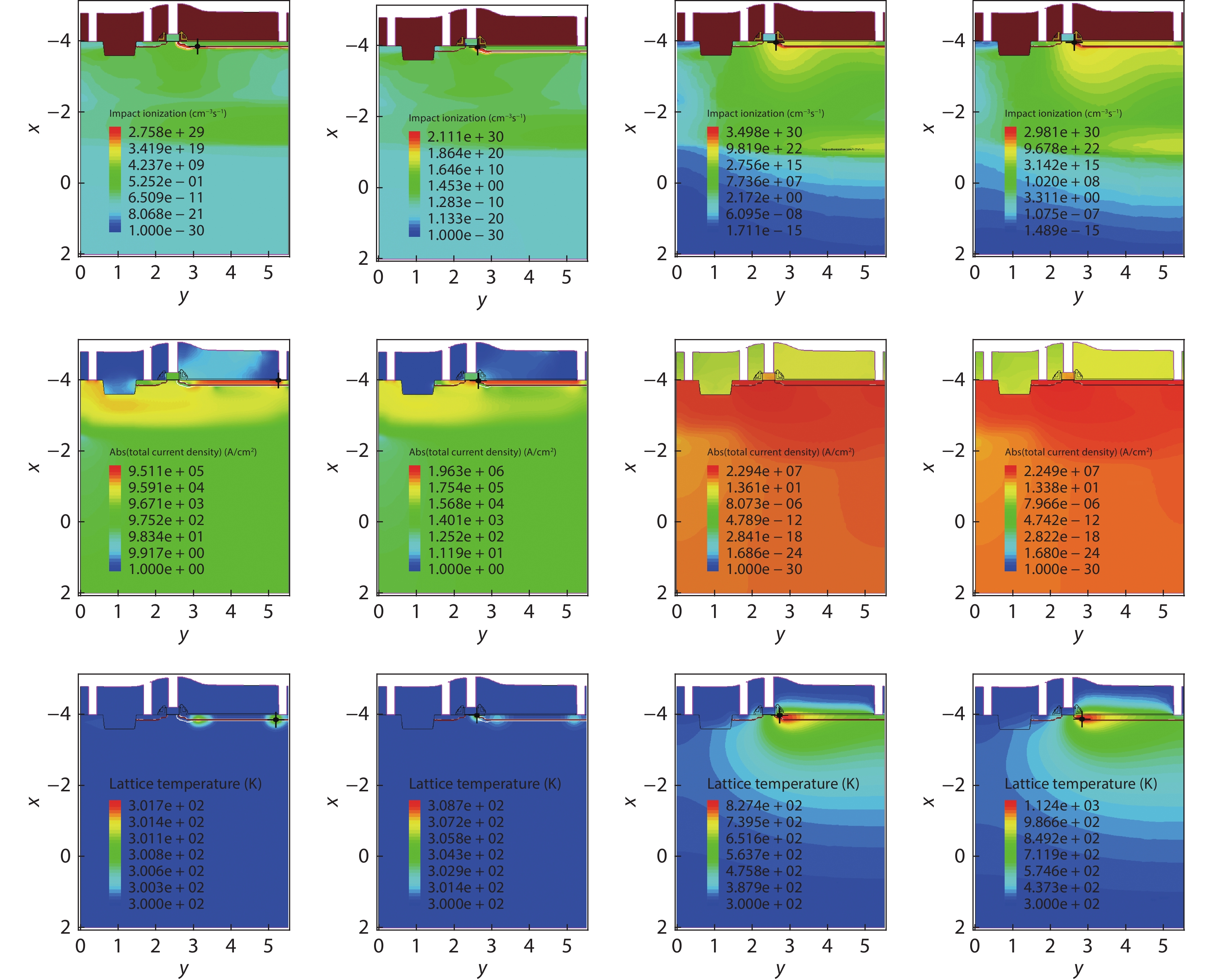
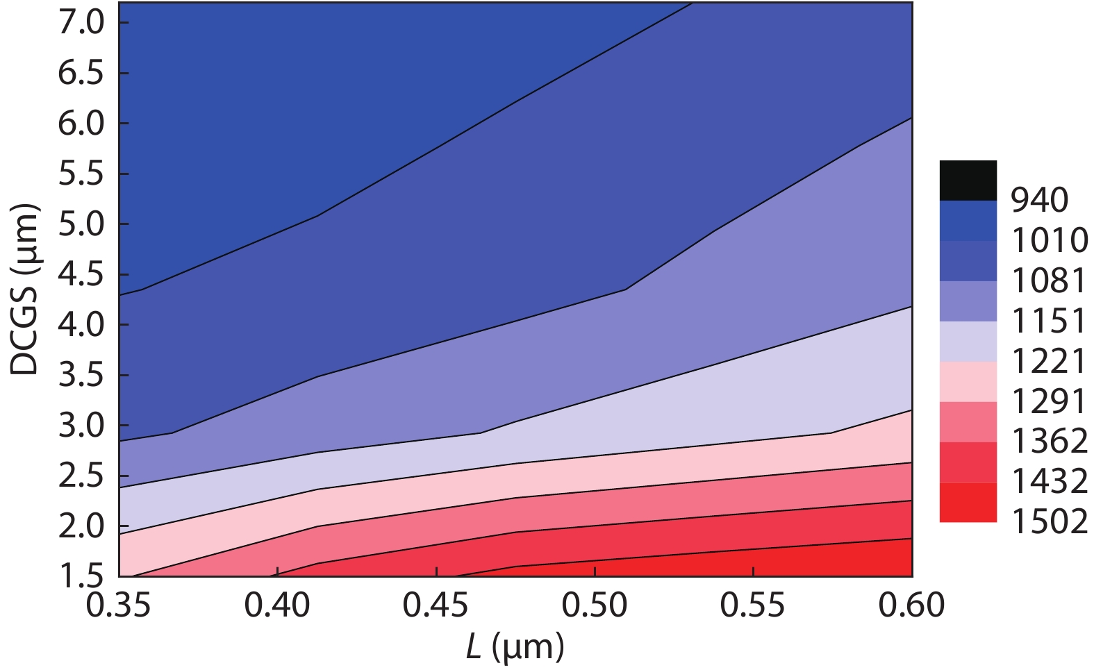
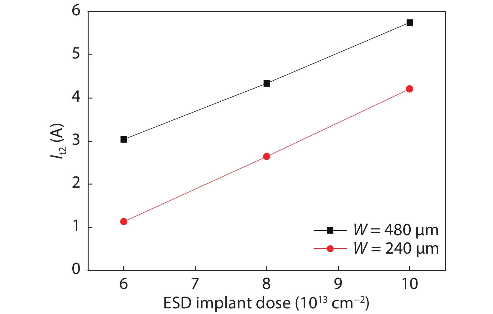
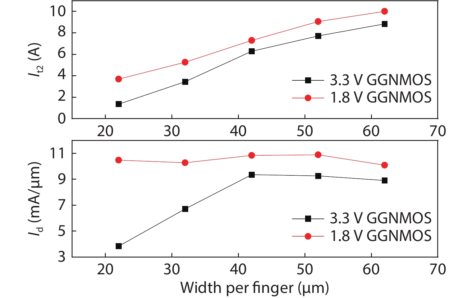
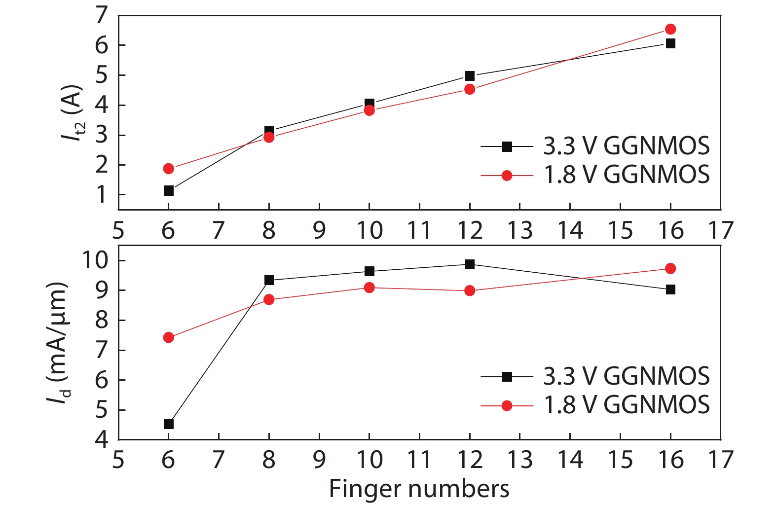
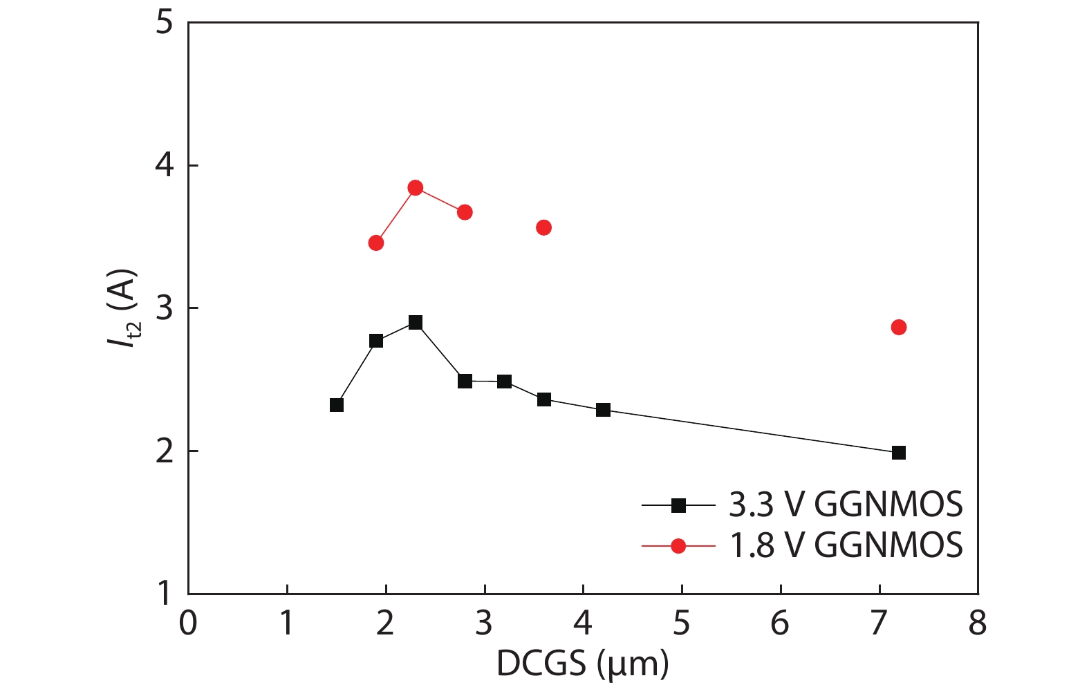
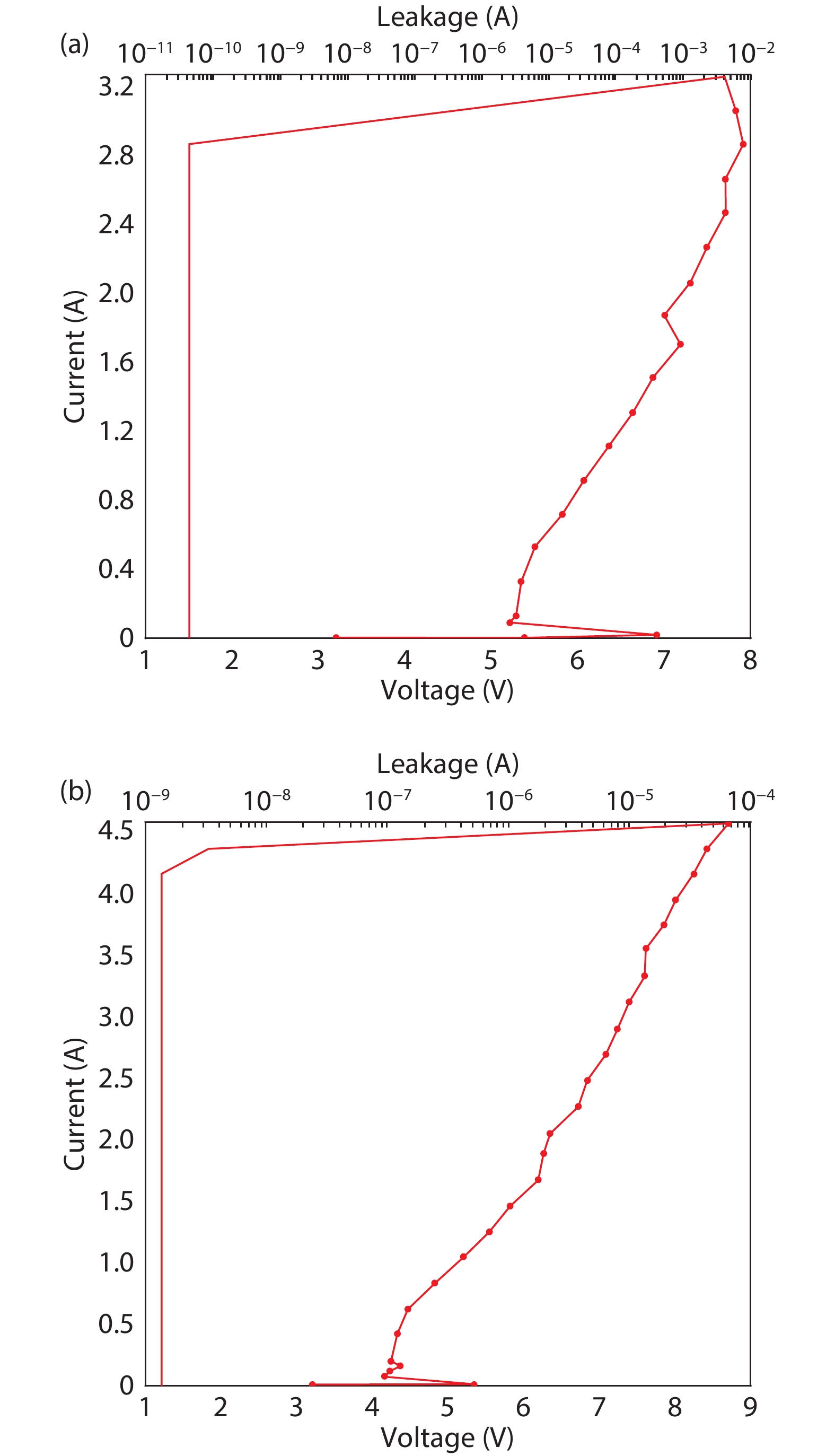
Table 1. The radiation-hardened 0.18 μm CMOS process characteristic parameters.
| Item | Feature |
| Minimum feature size | 0.18 μm undoped polysilicon gate |
| Operating voltage | Core device 1.8 V, IO device 3.3 V |
| Isolation technology | STI |
| Well structure | Double retrograded well |
| Spacer | Type LONO Spacer |
| Gate oxide | Dual gate oxide |
| Silicide | Fully self aligned CoSi2 gate, source, drain |
| Interconnection | Aluminum interconnection with tungsten plug technology HDP low-K FSG IMD |
| Optional device | DN, HR, MIM optional |
| Reliability | ≥ 20 years |
| TID | ≥ 300 krad (Si) |
| SEL | ≥ 75 MeV·cm2/mg |
| SEU | ≤ 1 × 10⁻¹⁰ error /(bit·day) (with standard library) |
 DownLoad: CSV
Table 2. Comparison with literature.
| GGNMOS device | Single finger width (μm) | Multi finger number | Total width (μm) | Vt2 (V) | It2 (A) | Discharge efficiency | Reference |
| 3.3 Va | 40 | 6 | 240 | 7.60 | 2.90 | 12.08 | / |
| 1.8 Va | 40 | 6 | 240 | 8.61 | 3.84 | 16.0 | / |
| 1.8 V | 40 | 8 | 320 | 20.27 | 4.55 | 14.2 | [17] |
| 3.3 V | 60 | 6 | 360 | / | 3 (≥ 4500 V) | 8.33 | [18] |
| 3.3 V | 30 | 12 | 360 | / | 1 (≥ 1500 V) | 2.78 | [18] |
| 3.3 V | 60 | 12 | 720 | / | 3 (≥ 8000 V) | 7.4 | [18] |
| 3.3 V | 90 | 8 | 720 | 5.24 | 5.17 | 7.18 | [19] |
| 1.8 V | / | / | / | / | / | 9.1b | [1] |
| 3.3 V | / | / | / | / | / | 8.1b | [1] |
| a Indicate this work. b Published literature, Fig. 16. | |||||||
DownLoad: CSV
| [1] |
Kepens B. On-chip ESD solutions seminar. SOFICS, Shanghai, 2015
|
| [2] |
Xie R B, Ji X M, Wu J W. Research on ESD performance of devices in radiation hardening process. Microprocessors, 2019, 40, 1 doi: 10.3969/j.issn.1002-2279.2019.03.001
|
| [3] |
Wang A Z H. On-chip ESD protection for integrated circuits: An IC design perspective. Springer Science & Business Media, 2006
|
| [4] |
Zhang L Z, Wang Y, Wang Y Z, et al. Insight into multiple-triggering effect in DTSCRs for ESD protection. J Semicond, 2017, 38, 075001 doi: 10.1088/1674-4926/38/7/075001
|
| [5] |
Bi X W, Liang H L, Gu X F, et al. Design of novel DDSCR with embedded PNP structure for ESD protection. J Semicond, 2015, 36, 124007 doi: 10.1088/1674-4926/36/12/124007
|
| [6] |
Mohan N, Kumar A. ESD protection design methodology in deep sub-micron CMOS technologies. Project Report, Course E&CE 730 (Topic 9), 2003, 5
|
| [7] |
Jiang Y X, Li J, Ran F, et al. Influence of layout parameters on snapback characteristic for a gate-grounded NMOS device in 0.13-μm silicide CMOS technology. J Semicond, 2009, 30, 084007 doi: 10.1088/1674-4926/30/8/084007
|
| [8] |
Chen T Y, Ker M D. Analysis on the dependence of layout parameters on ESD robustness of CMOS devices for manufacturing in deep-submicron CMOS process. IEEE Trans Semicond Manuf, 2003, 16, 486 doi: 10.1109/TSM.2003.815200
|
| [9] |
Do K I, Park J G, Kwon M J, et al. Analysis of GGNMOS-based ESD protection device using DCGS variation with robustness. Academic Conference of Korean Institute of Electronic Engineering, 2016, 6, 74
|
| [10] |
Krabbenborg B, Beltman R, Wolbert P, et al. Physics of electro-thermal effects in ESD protection devices. J Electrost, 1992, 28, 285 doi: 10.1016/0304-3886(92)90077-7
|
| [11] |
Chen J Z, Zhang X Y, Amerasekera A, et al. Design and layout of a high ESD performance NPN structure for submicron BiCMOS/bipolar circuits. Proceedings of International Reliability Physics Symposium, 1996
|
| [12] |
Ker M D, Chen T Y. Substrate-triggered technique for on-chip ESD protection design in a 0.18-μm salicided CMOS process. IEEE Trans Electron Devices, 2003, 50, 1050 doi: 10.1109/TED.2003.812495
|
| [13] |
Wu D X, Jiang L L, Fan H, et al. Analysis on the positive dependence of channel length on ESD failure current of a GGNMOS in a 5 V CMOS. J Semicond, 2013, 34, 024004 doi: 10.1088/1674-4926/34/2/024004
|
| [14] |
Wu J W, Yu Z G, Hong G S, et al. A method for strengthening the total ionizing dose of 0.18 μm bulk CMOS process. 2018 International Conference on Radiation Effects of Electronic Devices, 2018
|
| [15] |
Paul M, Russ C, Kumar B S, et al. Physics of current filamentation in ggNMOS devices under ESD condition revisited. IEEE Trans Electron Devices, 2018, 65, 2981 doi: 10.1109/TED.2018.2835831
|
| [16] |
Wang Y, Lu G Y, Wang Y Z, et al. Power-rail ESD clamp circuit with parasitic-BJT and channel parallel shunt paths to achieve enhanced robustness. IEICE Trans Electron, 2017, E100.C, 344 doi: 10.1587/transele.E100.C.344
|
| [17] |
Li L, Zhu K H. ESD performance analysis of gate grounded NMOS devices. Electron Pack, 2011, 11, 18 doi: 10.3969/j.issn.1681-1070.2011.02.006
|
| [18] |
Li Z G, Yue S G, Sun Y Z. Research on ESD device design of deep submicron IC. The 16th National Conference on Silicon Materials for Semiconductor Integrated circuits, 2009
|
| [19] |
Li Z G, Yue S G, Sun Y S. GDNMOS design for ESD protection in submicron CMOS VLSI. 2009 Asia Pacific Conference on Postgraduate Research in Microelectronics & Electronics, 2009, 432
|
| [20] |
Shi J. Deep sub-micron ESD GGNMOS layout design and optimization. MATEC Web Conf, 2018, 198, 04009 doi: 10.1051/matecconf/201819804009
|
| [21] |
Boschke R, Chen S H, Scholz M, et al. ESD ballasting of Ge FinFET ggNMOS devices. 2017 IEEE International Reliability Physics Symposium (IRPS) – Monterey, 2017
|


Article views: 7873 Times PDF downloads: 473 Times Cited by: 0 Times
Received: 30 March 2020 Revised: 27 April 2020 Online: Accepted Manuscript: 18 June 2020Uncorrected proof: 19 June 2020Published: 08 December 2020
| Citation: |
Jianwei Wu, Zongguang Yu, Genshen Hong, Rubin Xie. Design of GGNMOS ESD protection device for radiation-hardened 0.18 μm CMOS process[J]. Journal of Semiconductors, 2020, 41(12): 122403. doi: 10.1088/1674-4926/41/12/122403
****
J W Wu, Z G Yu, G S Hong, R B Xie, Design of GGNMOS ESD protection device for radiation-hardened 0.18 μm CMOS process[J]. J. Semicond., 2020, 41(12): 122403. doi: 10.1088/1674-4926/41/12/122403.

|
| [1] |
Kepens B. On-chip ESD solutions seminar. SOFICS, Shanghai, 2015
|
| [2] |
Xie R B, Ji X M, Wu J W. Research on ESD performance of devices in radiation hardening process. Microprocessors, 2019, 40, 1 doi: 10.3969/j.issn.1002-2279.2019.03.001
|
| [3] |
Wang A Z H. On-chip ESD protection for integrated circuits: An IC design perspective. Springer Science & Business Media, 2006
|
| [4] |
Zhang L Z, Wang Y, Wang Y Z, et al. Insight into multiple-triggering effect in DTSCRs for ESD protection. J Semicond, 2017, 38, 075001 doi: 10.1088/1674-4926/38/7/075001
|
| [5] |
Bi X W, Liang H L, Gu X F, et al. Design of novel DDSCR with embedded PNP structure for ESD protection. J Semicond, 2015, 36, 124007 doi: 10.1088/1674-4926/36/12/124007
|
| [6] |
Mohan N, Kumar A. ESD protection design methodology in deep sub-micron CMOS technologies. Project Report, Course E&CE 730 (Topic 9), 2003, 5
|
| [7] |
Jiang Y X, Li J, Ran F, et al. Influence of layout parameters on snapback characteristic for a gate-grounded NMOS device in 0.13-μm silicide CMOS technology. J Semicond, 2009, 30, 084007 doi: 10.1088/1674-4926/30/8/084007
|
| [8] |
Chen T Y, Ker M D. Analysis on the dependence of layout parameters on ESD robustness of CMOS devices for manufacturing in deep-submicron CMOS process. IEEE Trans Semicond Manuf, 2003, 16, 486 doi: 10.1109/TSM.2003.815200
|
| [9] |
Do K I, Park J G, Kwon M J, et al. Analysis of GGNMOS-based ESD protection device using DCGS variation with robustness. Academic Conference of Korean Institute of Electronic Engineering, 2016, 6, 74
|
| [10] |
Krabbenborg B, Beltman R, Wolbert P, et al. Physics of electro-thermal effects in ESD protection devices. J Electrost, 1992, 28, 285 doi: 10.1016/0304-3886(92)90077-7
|
| [11] |
Chen J Z, Zhang X Y, Amerasekera A, et al. Design and layout of a high ESD performance NPN structure for submicron BiCMOS/bipolar circuits. Proceedings of International Reliability Physics Symposium, 1996
|
| [12] |
Ker M D, Chen T Y. Substrate-triggered technique for on-chip ESD protection design in a 0.18-μm salicided CMOS process. IEEE Trans Electron Devices, 2003, 50, 1050 doi: 10.1109/TED.2003.812495
|
| [13] |
Wu D X, Jiang L L, Fan H, et al. Analysis on the positive dependence of channel length on ESD failure current of a GGNMOS in a 5 V CMOS. J Semicond, 2013, 34, 024004 doi: 10.1088/1674-4926/34/2/024004
|
| [14] |
Wu J W, Yu Z G, Hong G S, et al. A method for strengthening the total ionizing dose of 0.18 μm bulk CMOS process. 2018 International Conference on Radiation Effects of Electronic Devices, 2018
|
| [15] |
Paul M, Russ C, Kumar B S, et al. Physics of current filamentation in ggNMOS devices under ESD condition revisited. IEEE Trans Electron Devices, 2018, 65, 2981 doi: 10.1109/TED.2018.2835831
|
| [16] |
Wang Y, Lu G Y, Wang Y Z, et al. Power-rail ESD clamp circuit with parasitic-BJT and channel parallel shunt paths to achieve enhanced robustness. IEICE Trans Electron, 2017, E100.C, 344 doi: 10.1587/transele.E100.C.344
|
| [17] |
Li L, Zhu K H. ESD performance analysis of gate grounded NMOS devices. Electron Pack, 2011, 11, 18 doi: 10.3969/j.issn.1681-1070.2011.02.006
|
| [18] |
Li Z G, Yue S G, Sun Y Z. Research on ESD device design of deep submicron IC. The 16th National Conference on Silicon Materials for Semiconductor Integrated circuits, 2009
|
| [19] |
Li Z G, Yue S G, Sun Y S. GDNMOS design for ESD protection in submicron CMOS VLSI. 2009 Asia Pacific Conference on Postgraduate Research in Microelectronics & Electronics, 2009, 432
|
| [20] |
Shi J. Deep sub-micron ESD GGNMOS layout design and optimization. MATEC Web Conf, 2018, 198, 04009 doi: 10.1051/matecconf/201819804009
|
| [21] |
Boschke R, Chen S H, Scholz M, et al. ESD ballasting of Ge FinFET ggNMOS devices. 2017 IEEE International Reliability Physics Symposium (IRPS) – Monterey, 2017
|

 WeChat ID
Journal of Semiconductors © 2017 All Rights Reserved 京ICP备05085259号-2