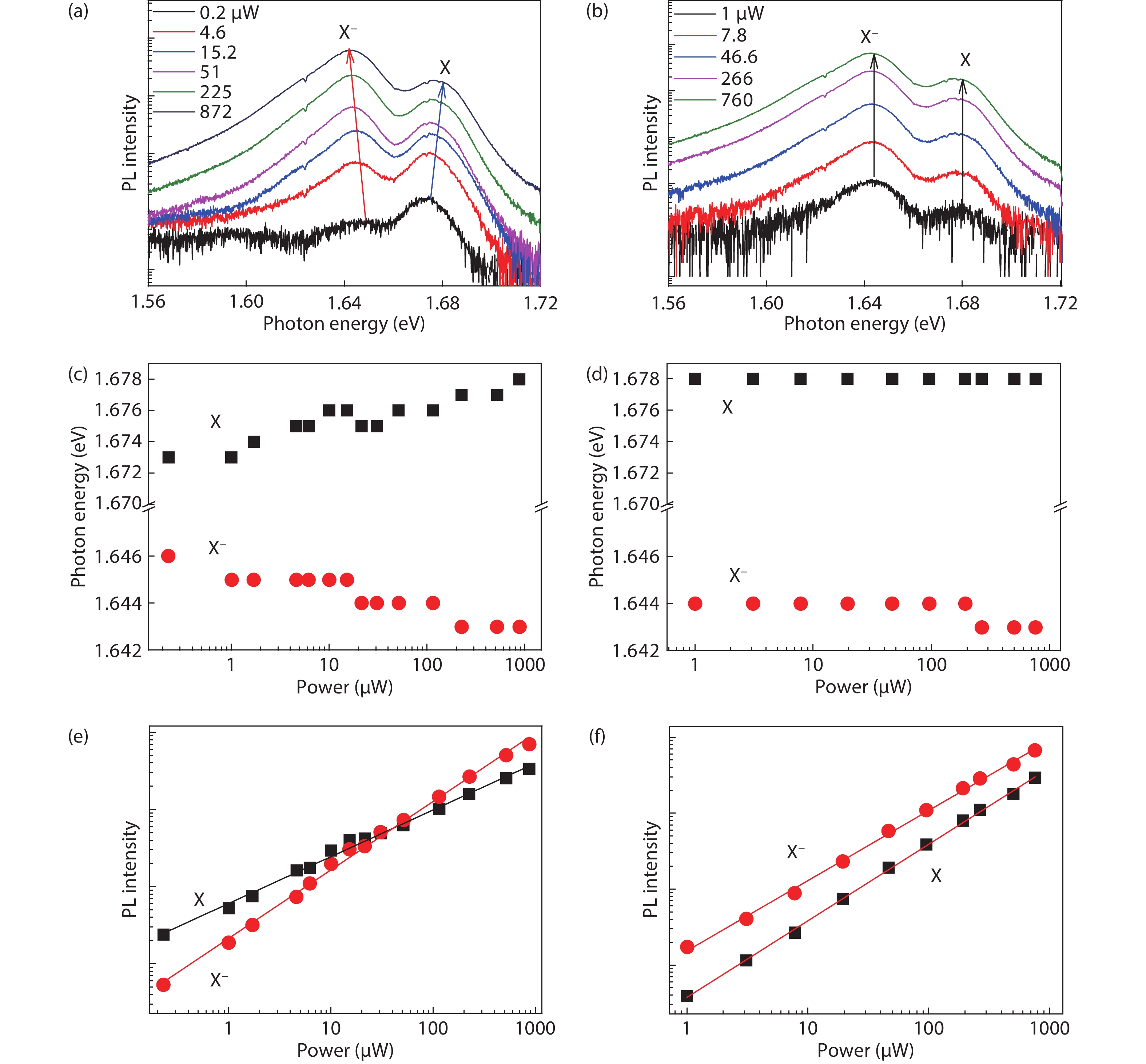
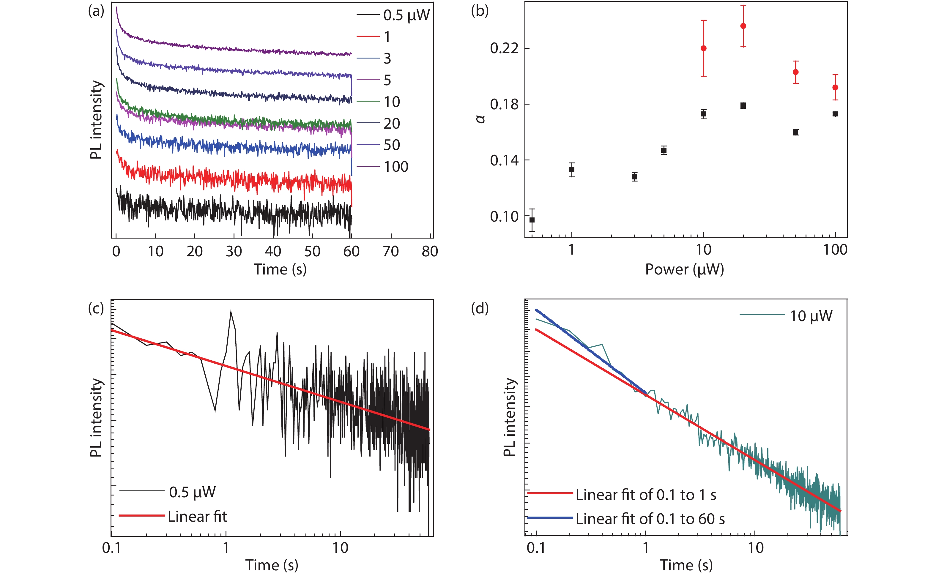
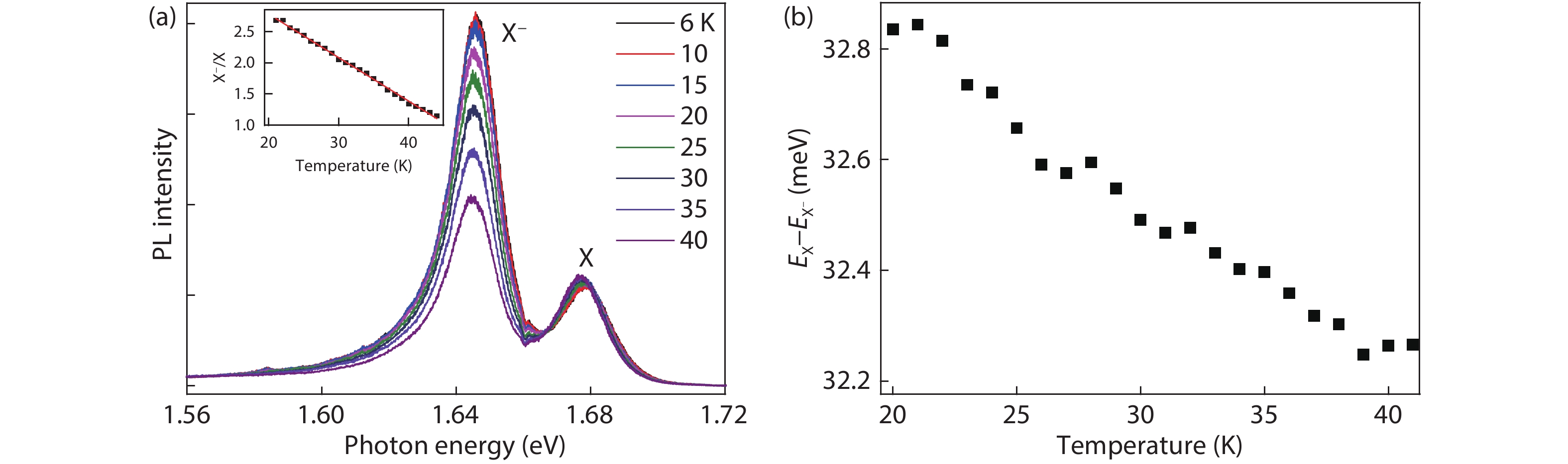
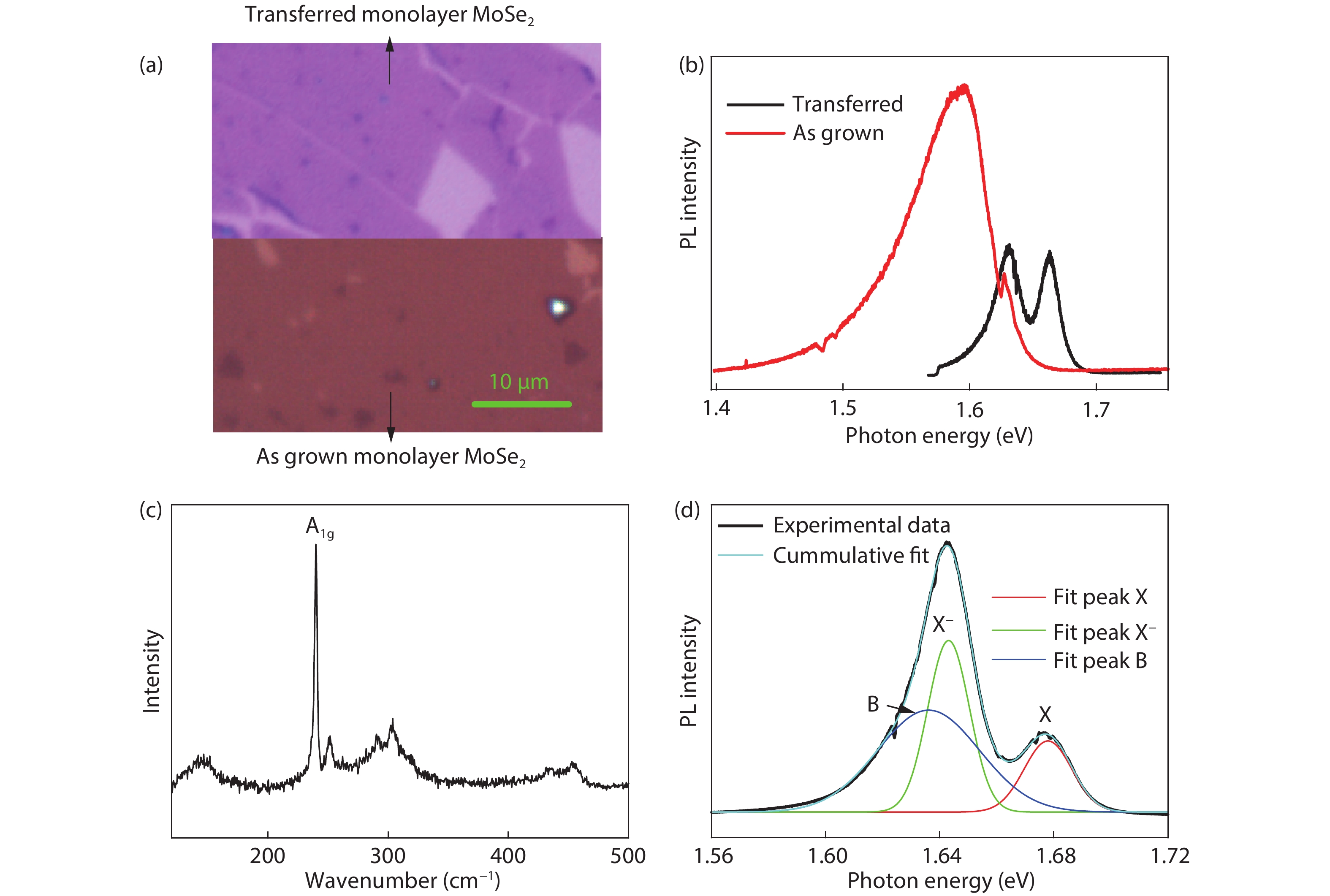
| [1] |
Salehzadeh O, Djavid M, Tran N H, et al. Optically pumped two-dimensional MoS 2 lasers operating at room-temperature. Nano Lett, 2015, 15, 5302 doi: 10.1021/acs.nanolett.5b01665 |
| [2] |
|
| [3] |
Wu S, Buckley S, Schaibley J R, et al. Monolayer semiconductor nanocavity lasers with ultralow thresholds. Nature, 2015, 520, 69 doi: 10.1038/nature14290 |
| [4] |
Pospischil A, Furchi M M, Mueller T. Solar-energy conversion and light emission in an atomic monolayer p–n diode. Nat Nanotechnol, 2014, 9, 257 doi: 10.1038/nnano.2014.14 |
| [5] |
Withers F, del Pozo-Zamudio O, Mishchenko A, et al. Light-emitting diodes by band-structure engineering in van der Waals heterostructures. Nat Mater, 2015, 14, 301 doi: 10.1038/nmat4205 |
| [6] |
Koperski M, Nogajewski K, Arora A, et al. Single photon emitters in exfoliated WSe 2 structures. Nat Nanotechnol, 2015, 10, 503 doi: 10.1038/nnano.2015.67 |
| [7] |
He Y M, Clark G, Schaibley J R, et al. Single quantum emitters in monolayer semiconductors. Nat Nanotechnol, 2015, 10, 497 doi: 10.1038/nnano.2015.75 |
| [8] |
Roldán R, Silva-Guillén J A, López-Sancho M P, et al. Electronic properties of single-layer and multilayer transition metal dichalcogenides MX 2 (M = Mo, W and X = S, Se). Ann Der Physik, 2014, 526, 347 doi: 10.1002/andp.201400128 |
| [9] |
Currie M, Hanbicki A T, Kioseoglou G, et al. Optical control of charged exciton states in tungsten disulfide. Appl Phys Lett, 2015, 106, 201907 doi: 10.1063/1.4921472 |
| [10] |
Singh A, Moody G, Tran K, et al. Trion formation dynamics in monolayer transition metal dichalcogenides. Phys Rev B, 2016, 93, 041401 doi: 10.1103/PhysRevB.93.041401 |
| [11] |
Godde T, Schmidt D, Schmutzler J, et al. Exciton and trion dynamics in atomically thin MoSe 2 and WSe 2: Effect of localization. Phys Rev B, 2016, 94, 165301 doi: 10.1103/PhysRevB.94.165301 |
| [12] |
Liu T, Xiang D, Zheng Y, et al. Nonvolatile and programmable photodoping in MoTe 2 for photoresist-free complementary electronic devices. Adv Mater, 2018, 30, 1804470 doi: 10.1002/adma.201804470 |
| [13] |
Quereda J, Ghiasi T S, van der Wal C H, et al. Semiconductor channel-mediated photodoping in h-BN encapsulated monolayer MoSe 2 phototransistors. 2D Mater, 2019, 6, 025040 doi: 10.1088/2053-1583/ab0c2d |
| [14] |
Ross J S, Wu S F, Yu H Y, et al. Electrical control of neutral and charged excitons in a monolayer semiconductor. Nat Commun, 2013, 4, 1474 doi: 10.1038/ncomms2498 |
| [15] |
Cadiz F, Robert C, Wang G, et al. Ultra-low power threshold for laser induced changes in optical properties of 2D molybdenum dichalcogenides. 2D Mater, 2016, 3, 045008 doi: 10.1088/2053-1583/3/4/045008 |
| [16] |
Atkin P, Lau D M, Zhang Q, et al. Laser exposure induced alteration of WS 2 monolayers in the presence of ambient moisture. 2D Mater, 2017, 5, 015013 doi: 10.1088/2053-1583/aa91b8 |
| [17] |
Liu Z, Amani M, Najmaei S, et al. Strain and structure heterogeneity in MoS 2 atomic layers grown by chemical vapour deposition. Nat Commun, 2014, 5, 5246 doi: 10.1038/ncomms6246 |
| [18] |
Fu X, Li F, Lin J F, et al. Pressure-dependent light emission of charged and neutral excitons in monolayer MoSe 2. J Phys Chem Lett, 2017, 8, 3556 doi: 10.1021/acs.jpclett.7b01374 |
| [19] |
Pei J, Yang J, Wang X, et al. Excited state biexcitons in atomically thin MoSe 2. ACS Nano, 2017, 11, 7468 doi: 10.1021/acsnano.7b03909 |
| [20] |
Lundt N, Cherotchenko E, Iff O, et al. The interplay between excitons and trions in a monolayer of MoSe 2. Appl Phys Lett, 2018, 112, 031107 doi: 10.1063/1.5019177 |
| [21] |
Pelant I, Valenta J. Luminescence spectroscopy of semiconductors. London: Oxford University Press, 2012
|
| [22] |
Scher H, Montroll E W. Anomalous transit-time dispersion in amorphous solids. Phys Rev B, 1975, 12, 2455 doi: 10.1103/PhysRevB.12.2455 |
| [23] |
Kakalios J, Street R A, Jackson W B. Stretched-exponential relaxation arising from dispersive diffusion of hydrogen in amorphous silicon. Phys Rev Lett, 1987, 59, 1037 doi: 10.1063/1.4933331 |


 DownLoad: