


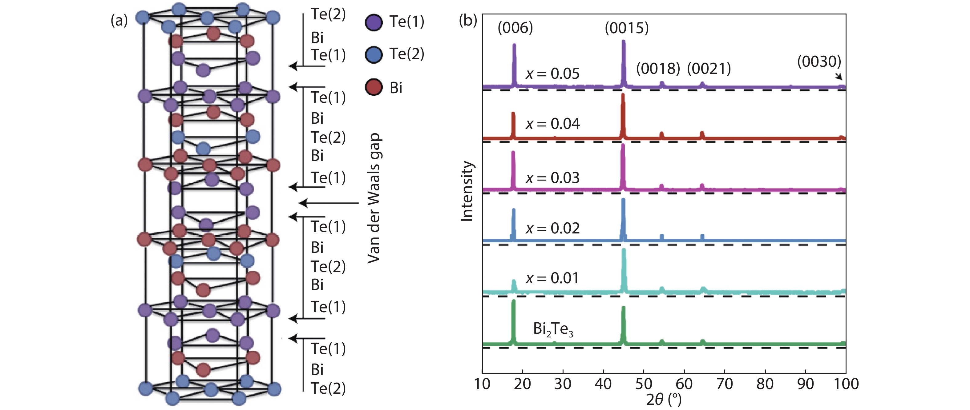
Fig. 1.
(Color online) (a) Schematic crystal structure of Bi2Te3. (b) XRD patterns of (CexBi1–x)2Te3 thin films (x = 0, 0.01, 0.02, 0.03, 0.04, 0.05).
ARTICLES
Peng Teng1, 2, 3, Tong Zhou4, Yonghuan Wang2, 3, Ke Zhao1, , Xiegang Zhu2, 3, and Xinchun Lai2
Corresponding author: Ke Zhao, zhaoke@swjtu.edu.cn; Xiegang Zhu, zhuxiegang@caep.cn
Abstract: Introducing magnetism into topological insulators (TIs) can tune the topological surface states and produce exotic physical effects. Rare earth elements are considered as important dopant candidates, due to their large magnetic moments from heavily shielded 4f electrons. As the first element with just one 4f electron, cerium (Ce) offers an ideal platform for exploring the doping effect of f-electron in TIs. Here in this work, we have grown cerium-doped topological insulator Bi2Te3 thin films on an Al2O3(0001) substrate by molecular beam epitaxy (MBE). Electronic transport measurements revealed the Kondo effect, weak anti-localization (WAL) effect and suppression of surface conducting channels by Ce doping. Our research shows the fundamental doping effects of Ce in Bi2Te3 thin films, and demonstrates that such a system could be a good platform for further research.
Keywords: topological insulators, molecular beam epitaxy, Kondo effect, weak anti-localization effect
| [1] |
Zhang H J, Liu C X, Qi X L, et al. Topological insulators in Bi2Se3, Bi2Te3, and Sb2Te3 with a single Dirac cone on the surface. Nat Phys, 2009, 5, 438 doi: 10.1038/nphys1270
|
| [2] |
Teo J, Fu L, Kane C L. Surface states and topological invariants in three-dimensional topological insulators: Application to Bi1− xSbx. Phys Rev B, 2008, 78, 045426 doi: 10.1103/PhysRevB.78.045426
|
| [3] |
Fu L, Kane C L. Topological insulators with inversion symmetry. Phys Rev B, 2007, 76, 045302 doi: 10.1103/PhysRevB.76.045302
|
| [4] |
Xia Y, Qian D, Hsieh D, et al. Observation of a large-gap topological-insulator class with a single Dirac cone on the surface. Nat Phys, 2009, 5, 398 doi: 10.1038/nphys1274
|
| [5] |
Chen Y L, Analytis J G, Chu J H, et al. Experimental realization of a three-dimensional topological insulator Bi2Te3. Science, 2009, 325, 178 doi: 10.1126/science.1173034
|
| [6] |
Hsieh D, Xia Y, Qian D, et al. Observation of time-reversal-protected single-cone topological insulator states in Bi2Te3 and Sb2Te3. Phys Rev Lett, 2009, 103, 146401 doi: 10.1103/PhysRevLett.103.146401
|
| [7] |
Yu R, Zhang W, Zhang H J, et al. Quantized anomalous Hall effect in magnetic topological insulators. Science, 2010, 329, 61 doi: 10.1126/science.1187485
|
| [8] |
Essin A M, Moore J E, Vanderbilt D. Magnetoelectric polarizability and axion electrodynamics in crystalline insulators. Phys Rev Lett, 2009, 102, 146805 doi: 10.1103/PhysRevLett.102.146805
|
| [9] |
Qi X L, Li R, Zang J, et al. Inducing a magnetic monopole with topological surface states. Science, 2009, 323, 1184 doi: 10.1126/science.1167747
|
| [10] |
Chang C Z, Zhang J, Feng X, et al. Experimental observation of the quantum anomalous Hall effect in a magnetic topological insulator. Science, 2013, 340, 167 doi: 10.1126/science.1234414
|
| [11] |
Collins-McIntyre L J, Watson M D, Baker A A, et al. X-ray magnetic spectroscopy of MBE-grown Mn-doped Bi2Se3 thin films. AIP Adv, 2014, 4, 127136 doi: 10.1063/1.4904900
|
| [12] |
Liu W, West D, He L, et al. Atomic-scale magnetism of Cr-doped Bi2Se3 thin film topological insulators. ACS Nano, 2015, 9, 10 doi: 10.1021/acsnano.5b03980
|
| [13] |
Li M, Chang C Z, Wu L, et al. Experimental verification of the van Vleck nature of long-range ferromagnetic order in the vanadium-doped three-dimensional topological insulator Sb2Te3. Phys Rev Lett, 2015, 114, 146802 doi: 10.1103/PhysRevLett.114.146802
|
| [14] |
Fan Y, Kou X, Upadhyaya P, et al. Electric-field control of spin–orbit torque in a magnetically doped topological insulator. Nat Nanotechnol, 2016, 11, 352 doi: 10.1038/nnano.2015.294
|
| [15] |
J Teng, N Liu, Y Q Li. Mn-doped topological insulators: a review. J Semicond, 2019, 40(8), 081507 doi: 10.1088/1674-4926/40/8/081507
|
| [16] |
Kou X, Pan L, Wang J, et al. Metal-to-insulator switching in quantum anomalous Hall states. Nat Commun, 2015, 6, 8474 doi: 10.1038/ncomms9474
|
| [17] |
Liang J, Yao X, Zhang Y J, et al. Formation of Fe-Te nanostructures during in situ Fe heavy doping of Bi2Te3. Nanomaterials, 2019, 9(5), 782 doi: 10.3390/nano9050782
|
| [18] |
Zimmermann S, Steckel F, Hess C, et al. Spin dynamics and magnetic interactions of Mn dopants in the topological insulator Bi2Te3. Phys Rev B, 2016, 94, 125205 doi: 10.1103/PhysRevB.94.125205
|
| [19] |
Wang H L, Ma J L, Wei Q Q, et al. Mn doping effects on the gate-tunable transport properties of Cd3As2 films epitaxied on GaAs. J Semicond, 2020, 41(7), 072903 doi: 10.1088/1674-4926/41/7/072903
|
| [20] |
Dietl T, Bonanni A, Ohno H. Families of magnetic semiconductors - an overview. J Semicond., 2019, 40(8), 080301 doi: 10.1088/1674-4926/40/8/080301
|
| [21] |
Hesjedal T. Rare earth doping of topological insulators: A brief review of thin film and heterostructure systems. Phys Status Solidi A, 2019, 216, 1800726 doi: 10.1002/pssa.201800726
|
| [22] |
Kim S W, Kim H, Kim J K, et al. Effect of antiferromagnetic order on topological electronic structure in Eu-substituted Bi2Se3 single crystals. APL Mater, 2020, 8, 111108 doi: 10.1063/5.0027947
|
| [23] |
Yue Z, Zhao W, Cortie D, et al. Modulation of crystal and electronic structures in topological insulators by rare-earth doping. ACS Appl Electron Mater, 2019, 1(9), 1929 doi: 10.1021/acsaelm.9b00422
|
| [24] |
Kim J, Lee K, Takabatake T, et al. Magnetic transition to antiferromagnetic phase in gadolinium substituted topological insulator Bi2Te3. Sci Rep, 2015, 5, 10309 doi: 10.1038/srep10309
|
| [25] |
Kim S W, Vrtnik S, Dolinše J, et al. Antiferromagnetic order induced by gadolinium substitution in Bi2Se3 single crystals. Appl Phys Lett, 2015, 106, 252401 doi: 10.1063/1.4922899
|
| [26] |
Lee H S, Kim J, Lee K, et al. Study of Ho-doped Bi2Te3 topological insulator thin films. Appl Phys Lett, 2015, 107, 182409 doi: 10.1063/1.4935120
|
| [27] |
Hikami S, Larkin A I, and Nagaoka Y. Spin-orbit interaction and magnetoresistance in the two dimensional random system. Prog Theor Phys, 1980, 63, 707 doi: 10.1143/PTP.63.707
|
| [28] |
Li Y Y, Wang G, Zhu X G, et al. Intrinsic topological insulator Bi2Te3 thin films on Si and their thickness limit. Adv Mater, 2010, 22(36), 4002 doi: 10.1002/adma.201000368
|
| [29] |
Hoefer K, Becker C, Rata D, et al. Intrinsic conduction through topological surface states of insulating Bi2Te3 epitaxial thin films. PNAS, 2014, 111(42), 14979 doi: 10.1073/pnas.1410591111
|
| [30] |
Wang G, Zhu X G, Sun Y Y, et al. Topological insulator thin films of Bi2Te3 with controlled electronic structure. Adv Mater, 2011, 23, 2929 doi: 10.1002/adma.201100678
|
| [31] |
Kondo J. Resistance minimum in dilute magnetic alloys. Prog Theor Phys, 1964, 32, 37 doi: 10.1143/PTP.32.37
|
| [32] |
He H T, Wang G, Zhang T, et al. Impurity effect on weak antilocalization in the topological insulator Bi2Te3. Phys Rev Lett, 2011, 106, 166805 doi: 10.1103/PhysRevLett.106.166805
|
| [33] |
Lu H Z, Shen S Q. Weak localization and weak anti-localization in topological insulators. Spintronics VII, 2014, 9167, 91672E
|
| [34] |
Kuntsevich A Y, Gabdullin A A, Prudkogliad V A, et al. Low-temperature Hall effect in bismuth chalcogenides thin films. Phys Rev B, 2016, 94, 235401 doi: 10.1103/PhysRevB.94.235401
|
| [35] |
Bao L, He L, Meyer N, et al. Weak anti-localization and quantum oscillations of surface states in topological insulator Bi2Se2Te. Sci Rep, 2012, 2, 726 doi: 10.1038/srep00726
|
| [36] |
Cha J J, Kong D S, Hong S S, et al. Weak antilocalization in Bi2(SexTe1– x)3 nanoribbons and nanoplates. Nano Lett, 2012, 12, 1107 doi: 10.1021/nl300018j
|
| [37] |
Gilbertson A M, Newaz A K M, Chang W J, et al. Dimensional crossover and weak localization in a 90 nm n-GaAs thin film. Appl Phys Lett, 2009, 95, 012113 doi: 10.1063/1.3176968
|
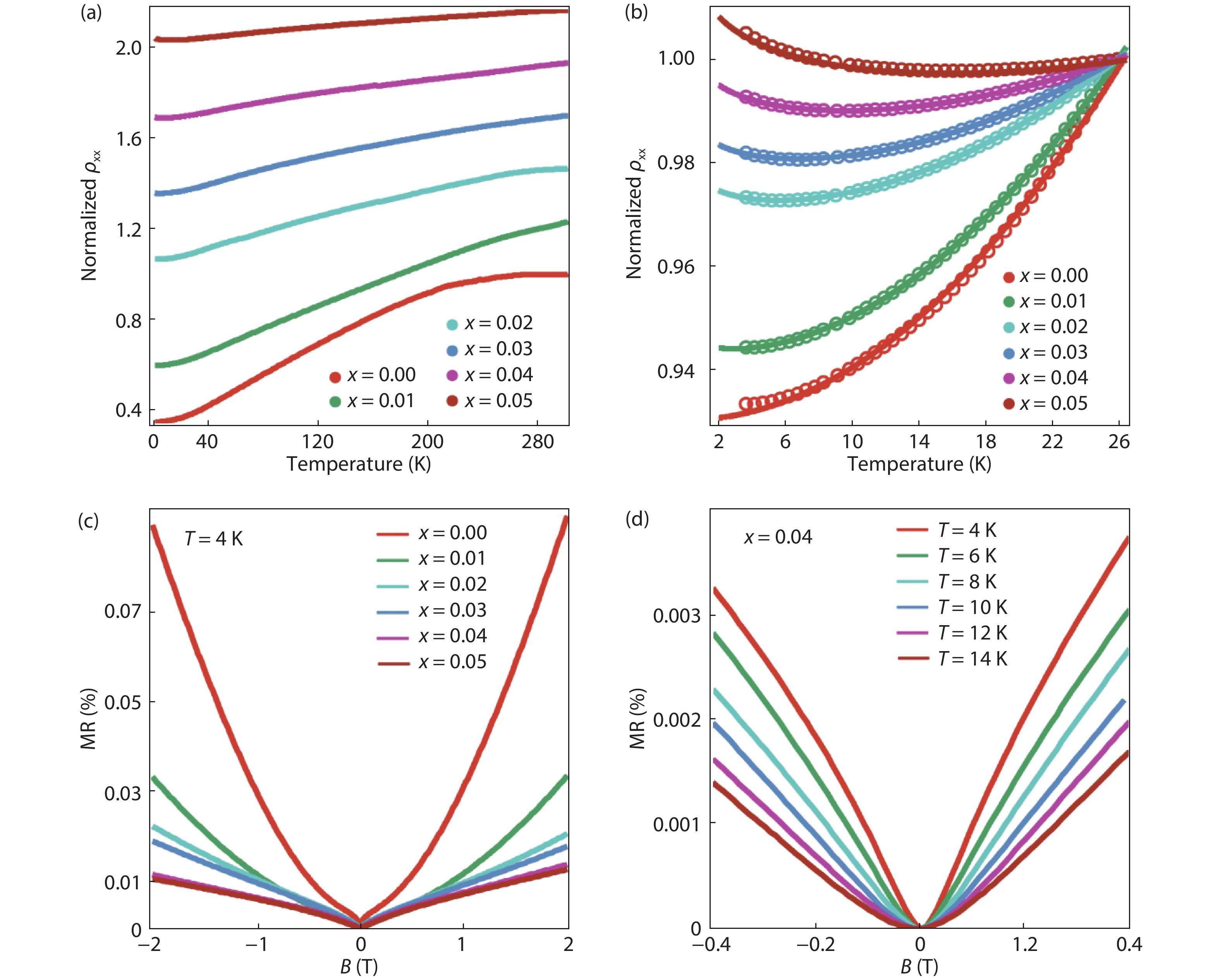
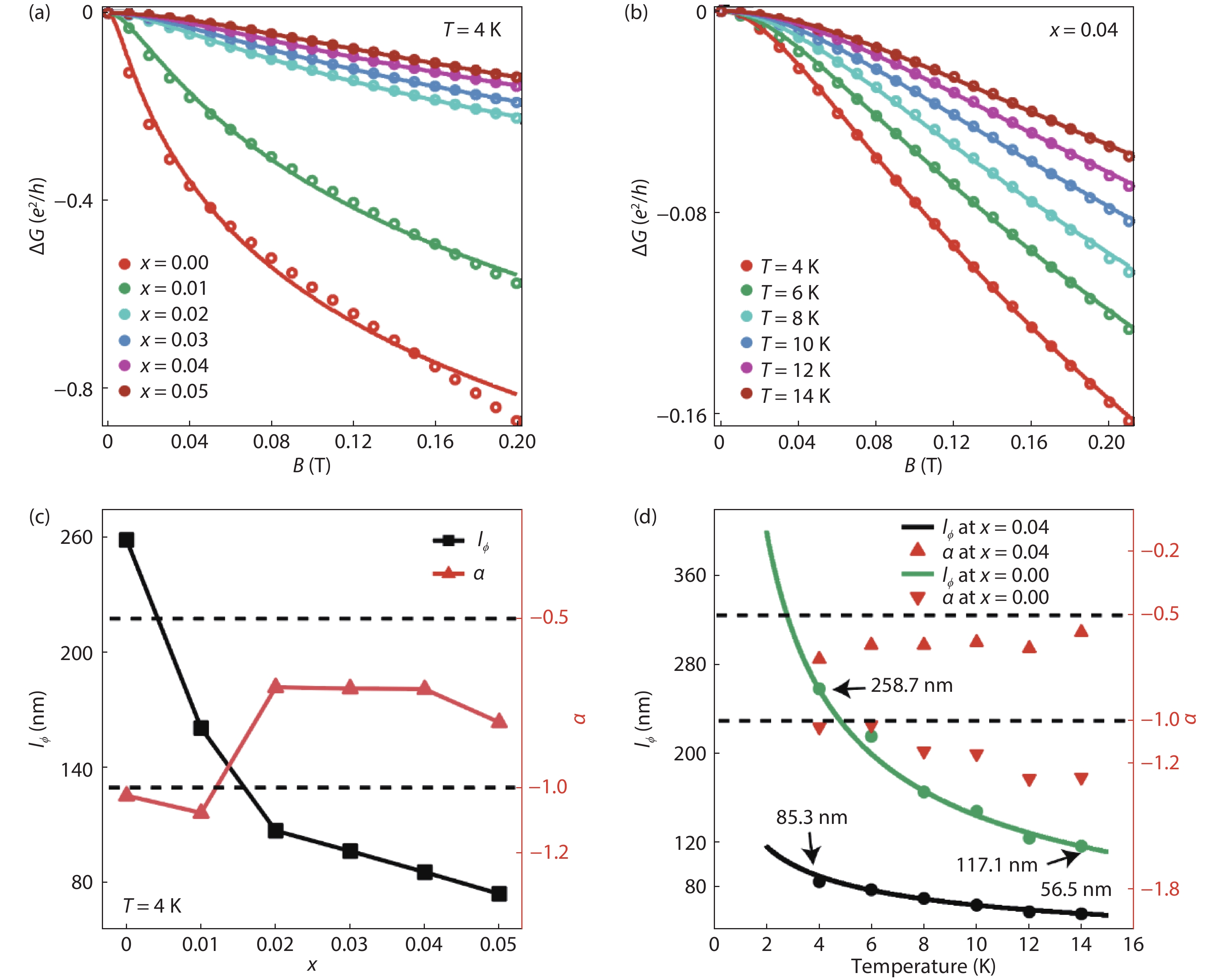
Table 1. Fitting results of the parameters in Eq. (1). All parameters are in corresponding SI units.
| Samples | ρ0 | A (10–5) | B (10–3) |
| x = 0 | 0.9303 | 10.59 | – |
| x = 0.01 | 0.945 | 9.39 | 1.607 |
| x = 0.02 | 0.9766 | 5.258 | 3.193 |
| x = 0.03 | 0.9858 | 4.053 | 3.62 |
| x = 0.04 | 0.9981 | 2.633 | 4.632 |
| x = 0.05 | 1.013 | 1.439 | 7.004 |
 DownLoad: CSV
Table 2.
Parameters extracted by fitting magnetoconductance data with Eqs. (3) and (5).
| (CexBi1–x)2Te3 | x = 0 | x = 0.01 | x = 0.02 | x = 0.03 | x = 0.04 | x = 0.05 |
| 258.7 | 160.5 | 107 | 96.3 | 85.3 | 73.9 | |
| 117.1 | 80.3 | 61.9 | 56.3 | 56.5 | 52.0 | |
| –1.027 | –1.079 | –0.704 | –0.708 | –0.709 | –0.809 | |
| –1.266 | –1.119 | –0.719 | –0.708 | –0.580 | –0.601 | |
| m | –0.633 | –0.5624 | –0.415 | –0.411 | –0.378 | –0.306 |
DownLoad: CSV
| [1] |
Zhang H J, Liu C X, Qi X L, et al. Topological insulators in Bi2Se3, Bi2Te3, and Sb2Te3 with a single Dirac cone on the surface. Nat Phys, 2009, 5, 438 doi: 10.1038/nphys1270
|
| [2] |
Teo J, Fu L, Kane C L. Surface states and topological invariants in three-dimensional topological insulators: Application to Bi1− xSbx. Phys Rev B, 2008, 78, 045426 doi: 10.1103/PhysRevB.78.045426
|
| [3] |
Fu L, Kane C L. Topological insulators with inversion symmetry. Phys Rev B, 2007, 76, 045302 doi: 10.1103/PhysRevB.76.045302
|
| [4] |
Xia Y, Qian D, Hsieh D, et al. Observation of a large-gap topological-insulator class with a single Dirac cone on the surface. Nat Phys, 2009, 5, 398 doi: 10.1038/nphys1274
|
| [5] |
Chen Y L, Analytis J G, Chu J H, et al. Experimental realization of a three-dimensional topological insulator Bi2Te3. Science, 2009, 325, 178 doi: 10.1126/science.1173034
|
| [6] |
Hsieh D, Xia Y, Qian D, et al. Observation of time-reversal-protected single-cone topological insulator states in Bi2Te3 and Sb2Te3. Phys Rev Lett, 2009, 103, 146401 doi: 10.1103/PhysRevLett.103.146401
|
| [7] |
Yu R, Zhang W, Zhang H J, et al. Quantized anomalous Hall effect in magnetic topological insulators. Science, 2010, 329, 61 doi: 10.1126/science.1187485
|
| [8] |
Essin A M, Moore J E, Vanderbilt D. Magnetoelectric polarizability and axion electrodynamics in crystalline insulators. Phys Rev Lett, 2009, 102, 146805 doi: 10.1103/PhysRevLett.102.146805
|
| [9] |
Qi X L, Li R, Zang J, et al. Inducing a magnetic monopole with topological surface states. Science, 2009, 323, 1184 doi: 10.1126/science.1167747
|
| [10] |
Chang C Z, Zhang J, Feng X, et al. Experimental observation of the quantum anomalous Hall effect in a magnetic topological insulator. Science, 2013, 340, 167 doi: 10.1126/science.1234414
|
| [11] |
Collins-McIntyre L J, Watson M D, Baker A A, et al. X-ray magnetic spectroscopy of MBE-grown Mn-doped Bi2Se3 thin films. AIP Adv, 2014, 4, 127136 doi: 10.1063/1.4904900
|
| [12] |
Liu W, West D, He L, et al. Atomic-scale magnetism of Cr-doped Bi2Se3 thin film topological insulators. ACS Nano, 2015, 9, 10 doi: 10.1021/acsnano.5b03980
|
| [13] |
Li M, Chang C Z, Wu L, et al. Experimental verification of the van Vleck nature of long-range ferromagnetic order in the vanadium-doped three-dimensional topological insulator Sb2Te3. Phys Rev Lett, 2015, 114, 146802 doi: 10.1103/PhysRevLett.114.146802
|
| [14] |
Fan Y, Kou X, Upadhyaya P, et al. Electric-field control of spin–orbit torque in a magnetically doped topological insulator. Nat Nanotechnol, 2016, 11, 352 doi: 10.1038/nnano.2015.294
|
| [15] |
J Teng, N Liu, Y Q Li. Mn-doped topological insulators: a review. J Semicond, 2019, 40(8), 081507 doi: 10.1088/1674-4926/40/8/081507
|
| [16] |
Kou X, Pan L, Wang J, et al. Metal-to-insulator switching in quantum anomalous Hall states. Nat Commun, 2015, 6, 8474 doi: 10.1038/ncomms9474
|
| [17] |
Liang J, Yao X, Zhang Y J, et al. Formation of Fe-Te nanostructures during in situ Fe heavy doping of Bi2Te3. Nanomaterials, 2019, 9(5), 782 doi: 10.3390/nano9050782
|
| [18] |
Zimmermann S, Steckel F, Hess C, et al. Spin dynamics and magnetic interactions of Mn dopants in the topological insulator Bi2Te3. Phys Rev B, 2016, 94, 125205 doi: 10.1103/PhysRevB.94.125205
|
| [19] |
Wang H L, Ma J L, Wei Q Q, et al. Mn doping effects on the gate-tunable transport properties of Cd3As2 films epitaxied on GaAs. J Semicond, 2020, 41(7), 072903 doi: 10.1088/1674-4926/41/7/072903
|
| [20] |
Dietl T, Bonanni A, Ohno H. Families of magnetic semiconductors - an overview. J Semicond., 2019, 40(8), 080301 doi: 10.1088/1674-4926/40/8/080301
|
| [21] |
Hesjedal T. Rare earth doping of topological insulators: A brief review of thin film and heterostructure systems. Phys Status Solidi A, 2019, 216, 1800726 doi: 10.1002/pssa.201800726
|
| [22] |
Kim S W, Kim H, Kim J K, et al. Effect of antiferromagnetic order on topological electronic structure in Eu-substituted Bi2Se3 single crystals. APL Mater, 2020, 8, 111108 doi: 10.1063/5.0027947
|
| [23] |
Yue Z, Zhao W, Cortie D, et al. Modulation of crystal and electronic structures in topological insulators by rare-earth doping. ACS Appl Electron Mater, 2019, 1(9), 1929 doi: 10.1021/acsaelm.9b00422
|
| [24] |
Kim J, Lee K, Takabatake T, et al. Magnetic transition to antiferromagnetic phase in gadolinium substituted topological insulator Bi2Te3. Sci Rep, 2015, 5, 10309 doi: 10.1038/srep10309
|
| [25] |
Kim S W, Vrtnik S, Dolinše J, et al. Antiferromagnetic order induced by gadolinium substitution in Bi2Se3 single crystals. Appl Phys Lett, 2015, 106, 252401 doi: 10.1063/1.4922899
|
| [26] |
Lee H S, Kim J, Lee K, et al. Study of Ho-doped Bi2Te3 topological insulator thin films. Appl Phys Lett, 2015, 107, 182409 doi: 10.1063/1.4935120
|
| [27] |
Hikami S, Larkin A I, and Nagaoka Y. Spin-orbit interaction and magnetoresistance in the two dimensional random system. Prog Theor Phys, 1980, 63, 707 doi: 10.1143/PTP.63.707
|
| [28] |
Li Y Y, Wang G, Zhu X G, et al. Intrinsic topological insulator Bi2Te3 thin films on Si and their thickness limit. Adv Mater, 2010, 22(36), 4002 doi: 10.1002/adma.201000368
|
| [29] |
Hoefer K, Becker C, Rata D, et al. Intrinsic conduction through topological surface states of insulating Bi2Te3 epitaxial thin films. PNAS, 2014, 111(42), 14979 doi: 10.1073/pnas.1410591111
|
| [30] |
Wang G, Zhu X G, Sun Y Y, et al. Topological insulator thin films of Bi2Te3 with controlled electronic structure. Adv Mater, 2011, 23, 2929 doi: 10.1002/adma.201100678
|
| [31] |
Kondo J. Resistance minimum in dilute magnetic alloys. Prog Theor Phys, 1964, 32, 37 doi: 10.1143/PTP.32.37
|
| [32] |
He H T, Wang G, Zhang T, et al. Impurity effect on weak antilocalization in the topological insulator Bi2Te3. Phys Rev Lett, 2011, 106, 166805 doi: 10.1103/PhysRevLett.106.166805
|
| [33] |
Lu H Z, Shen S Q. Weak localization and weak anti-localization in topological insulators. Spintronics VII, 2014, 9167, 91672E
|
| [34] |
Kuntsevich A Y, Gabdullin A A, Prudkogliad V A, et al. Low-temperature Hall effect in bismuth chalcogenides thin films. Phys Rev B, 2016, 94, 235401 doi: 10.1103/PhysRevB.94.235401
|
| [35] |
Bao L, He L, Meyer N, et al. Weak anti-localization and quantum oscillations of surface states in topological insulator Bi2Se2Te. Sci Rep, 2012, 2, 726 doi: 10.1038/srep00726
|
| [36] |
Cha J J, Kong D S, Hong S S, et al. Weak antilocalization in Bi2(SexTe1– x)3 nanoribbons and nanoplates. Nano Lett, 2012, 12, 1107 doi: 10.1021/nl300018j
|
| [37] |
Gilbertson A M, Newaz A K M, Chang W J, et al. Dimensional crossover and weak localization in a 90 nm n-GaAs thin film. Appl Phys Lett, 2009, 95, 012113 doi: 10.1063/1.3176968
|


Article views: 3316 Times PDF downloads: 109 Times Cited by: 0 Times
Received: 26 May 2021 Revised: 31 May 2021 Online: Accepted Manuscript: 09 July 2021Uncorrected proof: 19 July 2021Published: 03 December 2021
| Citation: |
Peng Teng, Tong Zhou, Yonghuan Wang, Ke Zhao, Xiegang Zhu, Xinchun Lai. Electrical transport properties of cerium doped Bi2Te3 thin films grown by molecular beam epitaxy[J]. Journal of Semiconductors, 2021, 42(12): 122902. doi: 10.1088/1674-4926/42/12/122902
****
P Teng, T Zhou, Y H Wang, K Zhao, X G Zhu, X C Lai, Electrical transport properties of cerium doped Bi2Te3 thin films grown by molecular beam epitaxy[J]. J. Semicond., 2021, 42(12): 122902. doi: 10.1088/1674-4926/42/12/122902.

|
| [1] |
Zhang H J, Liu C X, Qi X L, et al. Topological insulators in Bi2Se3, Bi2Te3, and Sb2Te3 with a single Dirac cone on the surface. Nat Phys, 2009, 5, 438 doi: 10.1038/nphys1270
|
| [2] |
Teo J, Fu L, Kane C L. Surface states and topological invariants in three-dimensional topological insulators: Application to Bi1− xSbx. Phys Rev B, 2008, 78, 045426 doi: 10.1103/PhysRevB.78.045426
|
| [3] |
Fu L, Kane C L. Topological insulators with inversion symmetry. Phys Rev B, 2007, 76, 045302 doi: 10.1103/PhysRevB.76.045302
|
| [4] |
Xia Y, Qian D, Hsieh D, et al. Observation of a large-gap topological-insulator class with a single Dirac cone on the surface. Nat Phys, 2009, 5, 398 doi: 10.1038/nphys1274
|
| [5] |
Chen Y L, Analytis J G, Chu J H, et al. Experimental realization of a three-dimensional topological insulator Bi2Te3. Science, 2009, 325, 178 doi: 10.1126/science.1173034
|
| [6] |
Hsieh D, Xia Y, Qian D, et al. Observation of time-reversal-protected single-cone topological insulator states in Bi2Te3 and Sb2Te3. Phys Rev Lett, 2009, 103, 146401 doi: 10.1103/PhysRevLett.103.146401
|
| [7] |
Yu R, Zhang W, Zhang H J, et al. Quantized anomalous Hall effect in magnetic topological insulators. Science, 2010, 329, 61 doi: 10.1126/science.1187485
|
| [8] |
Essin A M, Moore J E, Vanderbilt D. Magnetoelectric polarizability and axion electrodynamics in crystalline insulators. Phys Rev Lett, 2009, 102, 146805 doi: 10.1103/PhysRevLett.102.146805
|
| [9] |
Qi X L, Li R, Zang J, et al. Inducing a magnetic monopole with topological surface states. Science, 2009, 323, 1184 doi: 10.1126/science.1167747
|
| [10] |
Chang C Z, Zhang J, Feng X, et al. Experimental observation of the quantum anomalous Hall effect in a magnetic topological insulator. Science, 2013, 340, 167 doi: 10.1126/science.1234414
|
| [11] |
Collins-McIntyre L J, Watson M D, Baker A A, et al. X-ray magnetic spectroscopy of MBE-grown Mn-doped Bi2Se3 thin films. AIP Adv, 2014, 4, 127136 doi: 10.1063/1.4904900
|
| [12] |
Liu W, West D, He L, et al. Atomic-scale magnetism of Cr-doped Bi2Se3 thin film topological insulators. ACS Nano, 2015, 9, 10 doi: 10.1021/acsnano.5b03980
|
| [13] |
Li M, Chang C Z, Wu L, et al. Experimental verification of the van Vleck nature of long-range ferromagnetic order in the vanadium-doped three-dimensional topological insulator Sb2Te3. Phys Rev Lett, 2015, 114, 146802 doi: 10.1103/PhysRevLett.114.146802
|
| [14] |
Fan Y, Kou X, Upadhyaya P, et al. Electric-field control of spin–orbit torque in a magnetically doped topological insulator. Nat Nanotechnol, 2016, 11, 352 doi: 10.1038/nnano.2015.294
|
| [15] |
J Teng, N Liu, Y Q Li. Mn-doped topological insulators: a review. J Semicond, 2019, 40(8), 081507 doi: 10.1088/1674-4926/40/8/081507
|
| [16] |
Kou X, Pan L, Wang J, et al. Metal-to-insulator switching in quantum anomalous Hall states. Nat Commun, 2015, 6, 8474 doi: 10.1038/ncomms9474
|
| [17] |
Liang J, Yao X, Zhang Y J, et al. Formation of Fe-Te nanostructures during in situ Fe heavy doping of Bi2Te3. Nanomaterials, 2019, 9(5), 782 doi: 10.3390/nano9050782
|
| [18] |
Zimmermann S, Steckel F, Hess C, et al. Spin dynamics and magnetic interactions of Mn dopants in the topological insulator Bi2Te3. Phys Rev B, 2016, 94, 125205 doi: 10.1103/PhysRevB.94.125205
|
| [19] |
Wang H L, Ma J L, Wei Q Q, et al. Mn doping effects on the gate-tunable transport properties of Cd3As2 films epitaxied on GaAs. J Semicond, 2020, 41(7), 072903 doi: 10.1088/1674-4926/41/7/072903
|
| [20] |
Dietl T, Bonanni A, Ohno H. Families of magnetic semiconductors - an overview. J Semicond., 2019, 40(8), 080301 doi: 10.1088/1674-4926/40/8/080301
|
| [21] |
Hesjedal T. Rare earth doping of topological insulators: A brief review of thin film and heterostructure systems. Phys Status Solidi A, 2019, 216, 1800726 doi: 10.1002/pssa.201800726
|
| [22] |
Kim S W, Kim H, Kim J K, et al. Effect of antiferromagnetic order on topological electronic structure in Eu-substituted Bi2Se3 single crystals. APL Mater, 2020, 8, 111108 doi: 10.1063/5.0027947
|
| [23] |
Yue Z, Zhao W, Cortie D, et al. Modulation of crystal and electronic structures in topological insulators by rare-earth doping. ACS Appl Electron Mater, 2019, 1(9), 1929 doi: 10.1021/acsaelm.9b00422
|
| [24] |
Kim J, Lee K, Takabatake T, et al. Magnetic transition to antiferromagnetic phase in gadolinium substituted topological insulator Bi2Te3. Sci Rep, 2015, 5, 10309 doi: 10.1038/srep10309
|
| [25] |
Kim S W, Vrtnik S, Dolinše J, et al. Antiferromagnetic order induced by gadolinium substitution in Bi2Se3 single crystals. Appl Phys Lett, 2015, 106, 252401 doi: 10.1063/1.4922899
|
| [26] |
Lee H S, Kim J, Lee K, et al. Study of Ho-doped Bi2Te3 topological insulator thin films. Appl Phys Lett, 2015, 107, 182409 doi: 10.1063/1.4935120
|
| [27] |
Hikami S, Larkin A I, and Nagaoka Y. Spin-orbit interaction and magnetoresistance in the two dimensional random system. Prog Theor Phys, 1980, 63, 707 doi: 10.1143/PTP.63.707
|
| [28] |
Li Y Y, Wang G, Zhu X G, et al. Intrinsic topological insulator Bi2Te3 thin films on Si and their thickness limit. Adv Mater, 2010, 22(36), 4002 doi: 10.1002/adma.201000368
|
| [29] |
Hoefer K, Becker C, Rata D, et al. Intrinsic conduction through topological surface states of insulating Bi2Te3 epitaxial thin films. PNAS, 2014, 111(42), 14979 doi: 10.1073/pnas.1410591111
|
| [30] |
Wang G, Zhu X G, Sun Y Y, et al. Topological insulator thin films of Bi2Te3 with controlled electronic structure. Adv Mater, 2011, 23, 2929 doi: 10.1002/adma.201100678
|
| [31] |
Kondo J. Resistance minimum in dilute magnetic alloys. Prog Theor Phys, 1964, 32, 37 doi: 10.1143/PTP.32.37
|
| [32] |
He H T, Wang G, Zhang T, et al. Impurity effect on weak antilocalization in the topological insulator Bi2Te3. Phys Rev Lett, 2011, 106, 166805 doi: 10.1103/PhysRevLett.106.166805
|
| [33] |
Lu H Z, Shen S Q. Weak localization and weak anti-localization in topological insulators. Spintronics VII, 2014, 9167, 91672E
|
| [34] |
Kuntsevich A Y, Gabdullin A A, Prudkogliad V A, et al. Low-temperature Hall effect in bismuth chalcogenides thin films. Phys Rev B, 2016, 94, 235401 doi: 10.1103/PhysRevB.94.235401
|
| [35] |
Bao L, He L, Meyer N, et al. Weak anti-localization and quantum oscillations of surface states in topological insulator Bi2Se2Te. Sci Rep, 2012, 2, 726 doi: 10.1038/srep00726
|
| [36] |
Cha J J, Kong D S, Hong S S, et al. Weak antilocalization in Bi2(SexTe1– x)3 nanoribbons and nanoplates. Nano Lett, 2012, 12, 1107 doi: 10.1021/nl300018j
|
| [37] |
Gilbertson A M, Newaz A K M, Chang W J, et al. Dimensional crossover and weak localization in a 90 nm n-GaAs thin film. Appl Phys Lett, 2009, 95, 012113 doi: 10.1063/1.3176968
|

 WeChat ID
Journal of Semiconductors © 2017 All Rights Reserved 京ICP备05085259号-2


