J. Semicond. > 2021, Volume 42 > Issue 2 > 020502

SHORT COMMUNICATION

62 GHz germanium photodetector with inductive gain peaking electrode for photonic receiving beyond 100 Gbaud

Dingyi Wu1, 2, Xiao Hu1, 2, Weizhong Li1, 2, Daigao Chen1, 2, Lei Wang1, 2, and Xi Xiao1, 2

+ Author Affiliations

 Corresponding author: Lei Wang, lwang@wri.com.cn

DOI: 10.1088/1674-4926/42/2/020502

PDF

Turn off MathJax

Silicon photonics has attracted a great deal of interest for integrated photonics systems due to its large-scale electronics–photonics integration on a chip by leveraging the fabrication process of the complementary-metal-oxide semiconductor (CMOS) foundries[1-5]. Germanium-on-silicon (Ge-on-Si) waveguide photodetector (PD) is an indispensable building block of silicon photonics technology which requires high sensitivity, large bandwidth, and low dark current. However, there is a tradeoff between the high sensitivity and large bandwidth. The inductive gain peaking technique in silicon photonics processes which is firstly proposed by Hochberg and co-authors demonstrated that the bandwidth of Ge-on-Si PD can be improved significantly without sacrificing responsivity and undesired effects[6-9]. Although the 3-dB bandwidth has achieved 60 GHz, the demonstrated electrical eye diagram rate is only up to 45 Gbit/s. The limited eye diagram bit rate may be attributed to the large signal phase delay with different frequency. In this work, by employing inductive gain peaking technique with suitable inductance for conventional vertical Ge-on-Si PD, the 100 Gbit/s non-return-to-zero (NRZ) on-off-keying (OOK) and 64 Gbaud four-level pulse amplitude modulation (PAM-4) clear open eye diagrams are firstly realized with 3-dB bandwidth of 62 GHz.

It has been proved that by utilizing an inductor to peaking the opto-electrical (OE) response of a PD, the 3-dB bandwidth can be increased[6, 7]. Fig. 1(a) shows the cross-sectional view of designed peaking Ge-on-Si PD. It is fabricated on a commercial standard silicon-on-insulator (SOI) platform, with 220 nm Si and 8 μm buried oxide (BOX) layers. A 500 nm height Ge film is grown on the 220 nm Si-layer, with its top 100 nm ion implanted by N+ for ohmic contact. The bottom 220-nm-thick Si waveguide is implanted by P and P+ for ohmic contact. The width and length of Ge are about 4 and 25 μm, respectively. Fig. 1(b) shows the current–voltage (IV) characteristics of peaking PD in dark illuminated state. The dark current are about 8 and 46 nA at –1 and –3 V bias voltages. To further simulate how the PD equivalent circuit respond to the added inductor, a precisely circuit model is introduced, as shown in the inset of Fig. 1(c). The CjPD, RPD, Cpad, Rload, Rpk, Cpk, Lpk represent capacitance of PD junction, resistance of PD junction, capacitance of RF pad, resistance of load, resistance of inductor, capacitance of inductor and inductance, respectively. Here, the typical internal responsivity of this vertical Ge-on-Si PD is evaluated to be 0.8 A/W at 1550 nm. Fig. 1(c) shows normalized RF response of vertical Ge-on-Si PD with small peaking, large peaking and without peaking. The designed vertical Ge-on-Si PD with the large inductance shows an obviously over-peaking near 34 GHz followed by a sharp drop and a 3-dB bandwidth of 57 GHz. On the other hand, the vertical Ge-on-Si PD with small inductance possesses smoothing peak curve, but has 3-dB bandwidth of large than 60 GHz. The over-peaking PD would result in seriously signal distortion, which is because of the non-uniform time delay for different frequencies in the transient response[6]. Here, the inductance is elaborately designed to be 300 pH to decease the phase shift. By using a commercial software, the full 3-dimensional electromagnetic simulation of the inductor was performed to design the physical parameters. The simulation model of our inductor has also considered the processes of commercial standard SOI platform. After fabricated by the silicon photonics Fab, the PD device will be characterized with small signal and large signal measurements. The calibration of the high-speed RF trail was implemented to reduce the contributions from GSG probes and coaxial cables. The 3-dB bandwidth test experiments were achieved by collecting the response of the S21 transmission parameter in the Lightwave Component Analyzer (LCA, Keysight N4373D) tool versus frequency. Fig. 1(d) shows the experimental and fitted result of normalized RF response of vertical Ge-on-Si PD. The inset in Fig. 1(d) is the optical micrograph of the designed vertical Ge-on-Si PD with small inductance. By fitting the experimental result of S21 transmission parameter under 0.45 mA photocurrent, the 3-dB bandwidth of 62 GHz is realized with –3 V bias voltage. In order to obtain the inductance of fabricated PD, the S11 parameters are measured from 100 MHz to 60 GHz using LCA under –3 V bias voltage. Figs. 1(e) and 1(f) shows experimental and fitted magnitude/phase part of the small signal S11 reflection parameters. The series resistance, total capacitance, and inductance of Ge-on-Si PD are extracted by fitting S11 scattering parameter data to the small signal RC-model. The fitting result exhibits good agreement with the measured scattering parameter data curve, which results in a junction capacitance CjPD of 35 fF, junction resistance RPD of 24 Ω, pad capacitance Cpad of 12 fF, inductor resistance Rpk of 0, inductor capacitance Cpk of 3 fF and inductance Lpk of 276 pH, respectively. The load resistance Rload is 50 Ω. As the aforementioned, the optimum inductance of the designed device is 300 pH. However, the fitting inductor is 276 pH, which is smaller than the optimum value.

Figure  1.  (Color online) (a) Cross-sectional view of designed peaking Ge-on-Si PD. (b) IV characteristics of designed peaking Ge-on-Si PD in dark illuminated state. (c) The simulated normalized S21 response of vertical Ge-on-Si PD with small peaking, large peaking and without peaking. (d) The experimental and fitted result of normalized RF response of vertical Ge-on-Si PD with small inductance, the inset is the optical micrograph of peaking PD. (e–f) The experimental and fitted magnitude/phase part of the small signal S11 reflection parameters from 100 MHz to 60 GHz at –3 V bias voltage, the blue and red line represent experimental and fitted result, respectively.

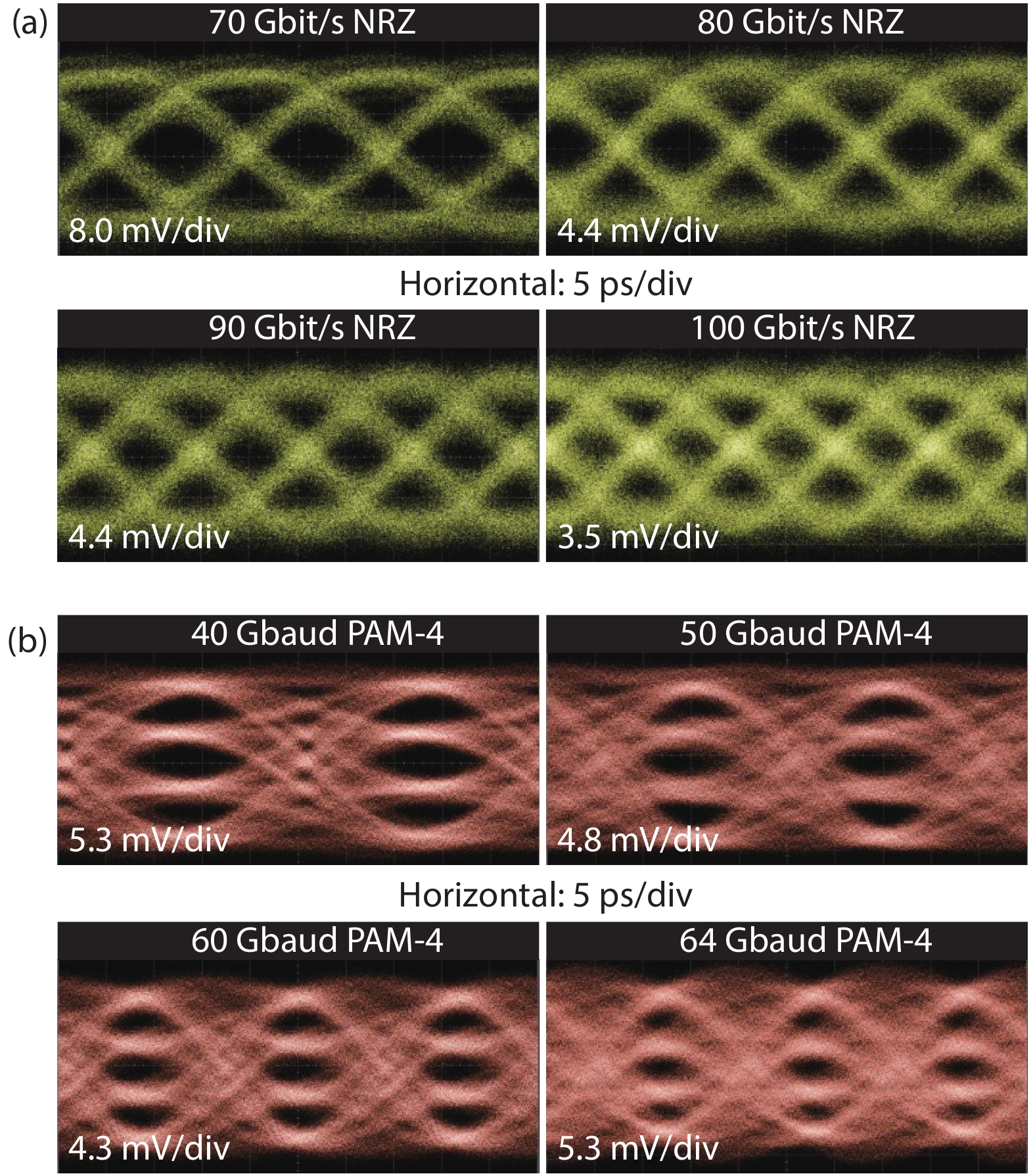
The feasibility of this Ge-on-Si PD with small inductance was further checked by measuring the eye-diagram large-signal acquisitions with different operation speed. The data were transmitted in NRZ and PAM-4 optical modulation formats. A 215 – 1 long optical NRZ pseudo random binary sequence (PRBS) data pattern at 70, 80, 90, 100 Gbit/s NRZ, and 40, 50, 60, 64 Gbaud PAM-4 generated by a commercial LiNbO3 modulator at 1550 nm was amplified by using a C-band erbium-doped fiber amplifier (EDFA), and followed by a filter (wavelength selective switch-WSS) to reduce spontaneous emission noise. As shown in Fig. 2, the clear open electrical eye diagrams up to 70, 80, 90, 100 Gbit/s NRZ, and 40, 50, 60, 64 Gbaud PAM-4 are experimentally attained. The achieved large-signal eye diagram measurements in Fig. 2 indicate a favorable performance of Ge-on-Si PD with inductive gain peaking technique. We can believe that the proposed Ge-on-Si PD device possesses the great potential to achieve low-cost >100 Gbit/s data reception per lane for future 800 GbE transceiver.

Figure  2.  (Color online) (a) Measured 70, 80, 90, and 100 Gbit/s NRZ eye diagrams under 3 V reverse-bias voltage. (b) Measured 40, 50, 60, and 64 Gbaud PAM-4 eye diagrams under 3 V reverse-bias voltage.

In summary, by employing inductive gain peaking technique for conventional vertical Ge-on-Si PD, the 3-dB bandwidth of 62 GHz are realized with 276 pH inductors. Benefitting from the suitable inductance, for the first time, the clear open electrical eye diagrams up to 70, 80, 90, 100 Gbit/s NRZ, and 40, 50, 60, 64 Gbaud PAM-4 are experimentally attained. It proves the efficiency of inductive gain peaking technique for high-speed integrated silicon photonics systems.

This work was supported by National Key Research and Development Program of China (2019YFB2205201, 2019YFB2205203) and Hubei Technological Innovation Project (2019AAA054).


[1]
Soref R A. Silicon-based optoelectronics. Proc IEEE, 1993, 81, 1687 doi: 10.1109/5.248958
[2]
Miller D A B. Device requirements for optical interconnects to silicon chips. Proc IEEE, 2009, 97, 1166 doi: 10.1109/JPROC.2009.2014298
[3]
Asghari M, Krishnamoorthy A V. Energy-efficient communication. Nat Photonics, 2011, 5, 268 doi: 10.1038/nphoton.2011.68
[4]
Thomson D, Zilkie A, Bowers J E, et al. Roadmap on silicon photonics. J Opt, 2016, 18, 073003 doi: 10.1088/2040-8978/18/7/073003
[5]
Yamada K, Tsuchizawa T, Nishi H, et al. High-performance silicon photonics technology for telecommunications applications. Sci Technol Adv Mater, 2014, 15, 024603 doi: 10.1088/1468-6996/15/2/024603
[6]
Gould M, Baehr-Jones T, Ding R, et al. Bandwidth enhancement of waveguide-coupled photodetectors with inductive gain peaking. Opt Express, 2012, 20, 7101 doi: 10.1364/OE.20.007101
[7]
Novack A, Gould M, Yang Y, et al. Germanium photodetector with 60 GHz bandwidth using inductive gain peaking. Opt Express, 2013, 21, 28387 doi: 10.1364/OE.21.028387
[8]
Chen G, Yu Y, Deng S, et al. Bandwidth improvement for germanium photodetector using wire bonding technology. Opt Express, 2015, 23, 25700 doi: 10.1364/OE.23.025700
[9]
Fard M M, Cowan G, Liboiron-Ladouceur O. Responsivity optimization of a high-speed germanium-on-silicon photodetector. Opt Express, 2016, 24, 27738 doi: 10.1364/OE.24.027738
Fig. 1.  (Color online) (a) Cross-sectional view of designed peaking Ge-on-Si PD. (b) IV characteristics of designed peaking Ge-on-Si PD in dark illuminated state. (c) The simulated normalized S21 response of vertical Ge-on-Si PD with small peaking, large peaking and without peaking. (d) The experimental and fitted result of normalized RF response of vertical Ge-on-Si PD with small inductance, the inset is the optical micrograph of peaking PD. (e–f) The experimental and fitted magnitude/phase part of the small signal S11 reflection parameters from 100 MHz to 60 GHz at –3 V bias voltage, the blue and red line represent experimental and fitted result, respectively.

Fig. 2.  (Color online) (a) Measured 70, 80, 90, and 100 Gbit/s NRZ eye diagrams under 3 V reverse-bias voltage. (b) Measured 40, 50, 60, and 64 Gbaud PAM-4 eye diagrams under 3 V reverse-bias voltage.

[1]
Soref R A. Silicon-based optoelectronics. Proc IEEE, 1993, 81, 1687 doi: 10.1109/5.248958
[2]
Miller D A B. Device requirements for optical interconnects to silicon chips. Proc IEEE, 2009, 97, 1166 doi: 10.1109/JPROC.2009.2014298
[3]
Asghari M, Krishnamoorthy A V. Energy-efficient communication. Nat Photonics, 2011, 5, 268 doi: 10.1038/nphoton.2011.68
[4]
Thomson D, Zilkie A, Bowers J E, et al. Roadmap on silicon photonics. J Opt, 2016, 18, 073003 doi: 10.1088/2040-8978/18/7/073003
[5]
Yamada K, Tsuchizawa T, Nishi H, et al. High-performance silicon photonics technology for telecommunications applications. Sci Technol Adv Mater, 2014, 15, 024603 doi: 10.1088/1468-6996/15/2/024603
[6]
Gould M, Baehr-Jones T, Ding R, et al. Bandwidth enhancement of waveguide-coupled photodetectors with inductive gain peaking. Opt Express, 2012, 20, 7101 doi: 10.1364/OE.20.007101
[7]
Novack A, Gould M, Yang Y, et al. Germanium photodetector with 60 GHz bandwidth using inductive gain peaking. Opt Express, 2013, 21, 28387 doi: 10.1364/OE.21.028387
[8]
Chen G, Yu Y, Deng S, et al. Bandwidth improvement for germanium photodetector using wire bonding technology. Opt Express, 2015, 23, 25700 doi: 10.1364/OE.23.025700
[9]
Fard M M, Cowan G, Liboiron-Ladouceur O. Responsivity optimization of a high-speed germanium-on-silicon photodetector. Opt Express, 2016, 24, 27738 doi: 10.1364/OE.24.027738
1

75 GHz germanium waveguide photodetector with 64 Gbps data rates utilizing an inductive-gain-peaking technique

Xiuli Li, Yupeng Zhu, Zhi Liu, Linzhi Peng, Xiangquan Liu, et al.

Journal of Semiconductors, 2023, 44(1): 012301. doi: 10.1088/1674-4926/44/1/012301

2

Precision photonic integration for future large-scale photonic integrated circuits

Xiangfei Chen

Journal of Semiconductors, 2019, 40(5): 050301. doi: 10.1088/1674-4926/40/5/050301

3

Strain effect on intersubband transitions in rolled-up quantum well infrared photodetectors

Han Wang, Shilong Li, Honglou Zhen, Xiaofei Nie, Gaoshan Huang, et al.

Journal of Semiconductors, 2017, 38(5): 054006. doi: 10.1088/1674-4926/38/5/054006

4

Photodetectors based on two dimensional materials

Zheng Lou, Zhongzhu Liang, Guozhen Shen

Journal of Semiconductors, 2016, 37(9): 091001. doi: 10.1088/1674-4926/37/9/091001

5

Progress in complementary metal-oxide-semiconductor silicon photonics and optoelectronic integrated circuits

Hongda Chen, Zan Zhang, Beiju Huang, Luhong Mao, Zanyun Zhang, et al.

Journal of Semiconductors, 2015, 36(12): 121001. doi: 10.1088/1674-4926/36/12/121001

6

AC-electronic and dielectric properties of semiconducting phthalocyanine compounds:a comparative study

Safa'a M. Hraibat, Rushdi M-L. Kitaneh, Mohammad M. Abu-Samreh, Abdelkarim M. Saleh

Journal of Semiconductors, 2013, 34(11): 112001. doi: 10.1088/1674-4926/34/11/112001

7

A different approach for determining the responsivity of n+p detectors using scanning electron microscopy

Omeime Xerviar Esebamen, Göran Thungström, Hans-Erik Nilsson

Journal of Semiconductors, 2012, 33(7): 074002. doi: 10.1088/1674-4926/33/7/074002

8

Photoconductive properties of lead iodide films prepared by electron beam evaporation

Zhu Xinghua, Yang Dingyu, Wei Zhaorong, Sun Hui, Wang Zhiguo, et al.

Journal of Semiconductors, 2010, 31(8): 083002. doi: 10.1088/1674-4926/31/8/083002

9

Photoelectric conversion characteristics of ZnO/SiC/Si heterojunctions

Wu Xiaopeng, Chen Xiaoqing, Sun Lijie, Mao Shun, Fu Zhuxi, et al.

Journal of Semiconductors, 2010, 31(10): 103002. doi: 10.1088/1674-4926/31/10/103002

10

A monolithic, standard CMOS, fully differential optical receiver with an integrated MSM photodetector

Yu Changliang, Mao Luhong, Xiao Xindong, Xie Sheng, Zhang Shilin, et al.

Journal of Semiconductors, 2009, 30(10): 105010. doi: 10.1088/1674-4926/30/10/105010

11

Optical properties in 1D photonic crystal structure using Si/C60 multilayers

Chen Jing, Tang Jiyu, Han Peide, Chen Junfang

Journal of Semiconductors, 2009, 30(4): 043001. doi: 10.1088/1674-4926/30/4/043001

12

Influence of zinc phthalocyanines on photoelectrical properties of hydrogenated amorphous silicon

Zhang Changsha, Zeng Xiangbo, Peng Wenbo, Shi Mingji, Liu Shiyong, et al.

Journal of Semiconductors, 2009, 30(8): 083004. doi: 10.1088/1674-4926/30/8/083004

13

Facile fabrication of UV photodetectors based on ZnO nanorod networks across trenched electrodes

Li Yingying, Cheng Chuanwei, Dong Xiang, Gao Junshan, Zhang Haiqian, et al.

Journal of Semiconductors, 2009, 30(6): 063004. doi: 10.1088/1674-4926/30/6/063004

14

An All-E-Beam Lithography Process for the Patterningof 2D Photonic Crystal Waveguide Devices

Yu Hejun, Yu Jinzhong, Chen Shaowu

Chinese Journal of Semiconductors , 2006, 27(11): 1894-1899.

15

Analysis of PTCDA/ITO Surface and Interface Using X-ray Photoelectron Spectroscopy and Atomic Force Microscopy

Tang Ning, Shen Bo, Wang Maojun, Yang Zhijian, Xu Ke, et al.

Chinese Journal of Semiconductors , 2006, 27(2): 235-238.

16

Analysis of PTCDA/ITO Surface and Interface Using X-ray Photoelectron Spectroscopy and Atomic Force Microscopy

Ou Guping, Song Zhen, Gui Wenming, Zhang Fujia

Chinese Journal of Semiconductors , 2006, 27(2): 229-234.

17

Photolithography Process Simulation for Integrated Circuitsand Microelectromechanical System Fabrication

Zhou Zaifa, Huang Qing'an, Li Weihua

Chinese Journal of Semiconductors , 2006, 27(4): 705-711.

18

Energy Transfer Probability Between Host and Guest in Doped Organic Electrophosphorescent Devices

Li Hongjian, Ouyang Jun, Dai Guozhang, Dai Xiaoyu, Pan Yanzhi, et al.

Chinese Journal of Semiconductors , 2006, 27(4): 674-678.

19

High-Integrated-Photosensitivity Negative-Electron-Affinity GaAs Photocathodes with Multilayer Be-Doping Structures

Wang Xiaofeng, Zeng Yiping, Wang Baoqiang, Zhu Zhanping, Du Xiaoqing, et al.

Chinese Journal of Semiconductors , 2005, 26(9): 1692-1698.

20

Fabrication of 1.55μm Si-Based Resonant Cavity Enhanced Photodetectors

Mao Rongwei, Zuo Yuhua, Li Chuanbo, Cheng Buwen, Teng Xuegong, et al.

Chinese Journal of Semiconductors , 2005, 26(2): 271-275.

1. Liang, Z., Shi, Y., Yi, Y. et al. Research on Electro-Optic Hybrid Multidigit Digital Multiplier Based on Surface Plasmon Polariton Technology. Photonics, 2024, 11(9): 785. doi:10.3390/photonics11090785
2. Alasio, M.G.C., Vallone, M., Tibaldi, A. et al. TCAD-Assisted Progress on the Cisco Platform Toward Low-Bias 200 Gbit/s vertical-pin Ge- on-Si Waveguide Photodetectors. Journal of Lightwave Technology, 2024, 42(9): 3269-3276. doi:10.1109/JLT.2024.3352437
3. Wang, Y., Sui, S., Gao, F. et al. Enhanced bandwidth of a lateral-pin Ge/Si avalanche photodiode using inductive gain peaking. Optics and Laser Technology, 2024. doi:10.1016/j.optlastec.2023.110445
4. Li, X., Xu, Q., Song, R. et al. High-uniformity and high-performance waveguide Ge photodetectors for the O and C bands. Applied Optics, 2024, 63(8): 2101-2108. doi:10.1364/AO.518425
5. Ruogu, S., Xinyu, L., Jinyu, W. et al. Lumped Folded Michelson Interferometer Modulators With Broadband Technologies. Journal of Lightwave Technology, 2023, 41(22): 6979-6986. doi:10.1109/JLT.2023.3295814
6. Hu, X., Wu, D., Liu, Y. et al. 408 Gbit/s PAM-8 sidewall-doped germanium–silicon photodetector. Photonics Research, 2023, 11(6): 961-967. doi:10.1364/PRJ.488166
7. Hu, X., Wu, D., Liu, Y. et al. 420 Gbit/s optical signal reception enabled by an inductive gain peaking Ge-Si photodetector with 80 GHz bandwidth. Optics Express, 2023, 31(11): 17987-17998. doi:10.1364/OE.486947
8. Wu, D., Wang, D., Chen, D. et al. Experimental demonstration of a 160 Gbit/s 3D-integrated silicon photonics receiver with 1.2-pJ/bit power consumption. Optics Express, 2023, 31(3): 4129-4139. doi:10.1364/OE.478852
9. Li, X., Zhu, Y., Liu, Z. et al. 75 GHz germanium waveguide photodetector with 64 Gbps data rates utilizing an inductive-gain-peaking technique. Journal of Semiconductors, 2023, 44(1): 012301. doi:10.1088/1674-4926/44/1/012301
10. Liu, Y., Sun, J., Song, R. et al. 80Gb/s NRZ Ge waveguide electro-absorption modulator. Optics Express, 2022, 30(19): 34276-34286. doi:10.1364/OE.462890
11. Li, S.-Y., Wang, L.-L., Wu, D. et al. High efficiency, small size, and large bandwidth vertical interlayer waveguide coupler. Chinese Physics B, 2022, 31(2): 024203. doi:10.1088/1674-1056/ac0dac
12. Wu, D., Wang, D., Chen, D. et al. A 128 Gbit/s 3D-Integrated Silicon Photonics Receiver with 1.5 pJ/bit Power Consumption. 2022. doi:10.1109/ACP55869.2022.10088619
13. Hao, Y., Wu, H., Yang, Y. et al. Preface to the special issue on beyond moore: Three-dimensional (3D) heterogeneous integration. Journal of Semiconductors, 2021, 42(2): 020101. doi:10.1088/1674-4926/42/2/020101
  • Search

    Advanced Search >>

    GET CITATION

    Dingyi Wu, Xiao Hu, Weizhong Li, Daigao Chen, Lei Wang, Xi Xiao. 62 GHz germanium photodetector with inductive gain peaking electrode for photonic receiving beyond 100 Gbaud[J]. Journal of Semiconductors, 2021, 42(2): 020502. doi: 10.1088/1674-4926/42/2/020502
    D Y Wu, X Hu, W Z Li, D G Chen, L Wang, X Xiao, 62 GHz germanium photodetector with inductive gain peaking electrode for photonic receiving beyond 100 Gbaud[J]. J. Semicond., 2021, 42(2): 020502. doi: 10.1088/1674-4926/42/2/020502.
    shu

    Export: BibTex EndNote

    Article Metrics

    Article views: 4123 Times PDF downloads: 179 Times Cited by: 13 Times

    History

    Received: 05 January 2021 Revised: 14 January 2021 Online: Uncorrected proof: 19 January 2021Accepted Manuscript: 19 January 2021Published: 08 February 2021

    Catalog

      Email This Article

      User name:
      Email:*请输入正确邮箱
      Code:*验证码错误
      Dingyi Wu, Xiao Hu, Weizhong Li, Daigao Chen, Lei Wang, Xi Xiao. 62 GHz germanium photodetector with inductive gain peaking electrode for photonic receiving beyond 100 Gbaud[J]. Journal of Semiconductors, 2021, 42(2): 020502. doi: 10.1088/1674-4926/42/2/020502 ****D Y Wu, X Hu, W Z Li, D G Chen, L Wang, X Xiao, 62 GHz germanium photodetector with inductive gain peaking electrode for photonic receiving beyond 100 Gbaud[J]. J. Semicond., 2021, 42(2): 020502. doi: 10.1088/1674-4926/42/2/020502.
      Citation:
      Dingyi Wu, Xiao Hu, Weizhong Li, Daigao Chen, Lei Wang, Xi Xiao. 62 GHz germanium photodetector with inductive gain peaking electrode for photonic receiving beyond 100 Gbaud[J]. Journal of Semiconductors, 2021, 42(2): 020502. doi: 10.1088/1674-4926/42/2/020502 ****
      D Y Wu, X Hu, W Z Li, D G Chen, L Wang, X Xiao, 62 GHz germanium photodetector with inductive gain peaking electrode for photonic receiving beyond 100 Gbaud[J]. J. Semicond., 2021, 42(2): 020502. doi: 10.1088/1674-4926/42/2/020502.

      62 GHz germanium photodetector with inductive gain peaking electrode for photonic receiving beyond 100 Gbaud

      DOI: 10.1088/1674-4926/42/2/020502
      More Information
      • Dingyi Wu:got his B.S. degree from Hubei University in 2017. Now he is a postgraduate student at Wuhan Research Institute of Posts and Telecommunications under the supervision of Prof. Xi Xiao. Since June 2019, he has been working in National Information Optoelectronics Innovation Center as a visiting student. His current re-search focuses on high-speed germanium-silicon photodetector
      • Xiao Hu:received the Ph.D. degree in Optical Engineering from the Wuhan National Laboratory for Optoelectronics, Huazhong University of Science and Technology, Wuhan, China, in 2017. He is currently a Senior Engineer with National Information Optoelectronics Innovation Center, China Information and Communication Technologies Group Corporation (CICT), Wuhan, China. His research efforts to innovations in photonic integrated devices and frontiers of high-speed/high-power germanium-silicon photodetectors, silicon hybrid integration modulators
      • Lei Wang:is a manager of silicon photonics R&D department in National Optoelectronics Innovation Center, leading a team and running a platform of silicon photonics research, test and product development. He has engaged in silicon photonics products development projects used in 5G, telecom and datacom. Prior to joining NOEIC, he is the vice director of silicon photonics group of State Key Laboratory of Optical Communication Technologies and Networks of CICT. He received a Ph.D. in Optoelectronic Information Engineering from Huazhong University of Science and Technology in 2012 and studied as a joint student in ECE department in University of Texas at Austin in 2010
      • Xi Xiao:received the B.S. and M.S. degrees from the Huazhong University of Science and Technology, Wuhan, China, in 2005 and 2007, respectively, and the Ph.D. degree from the Institute of Semiconductors, Chinese Academy of Sciences (ISCAS), Beijing, China, in 2010. He was an Assistant Professor and an Associate Professor with the Institute of Semiconductors, Chinese Academy of Sciences, from 2010 to 2013. He is currently the Director of the Silicon Photonics Lab, Fiber Home Technologies, Wuhan, the Vice Director of the State Key Laboratory of Optical Communication Technologies and Networks of China, and the CEO of the National Information Optoelectronics Innovation Center of China. His current research interests include the high-speed silicon-based PICs and EPICs for optical communication and optical interconnects, as well as their enabling fabrication and integration technologies
      • Corresponding author: lwang@wri.com.cn
      • Received Date: 2021-01-05
      • Revised Date: 2021-01-14
      • Published Date: 2021-02-10

      Catalog

        /

        DownLoad:  Full-Size Img  PowerPoint
        Return
        Return