


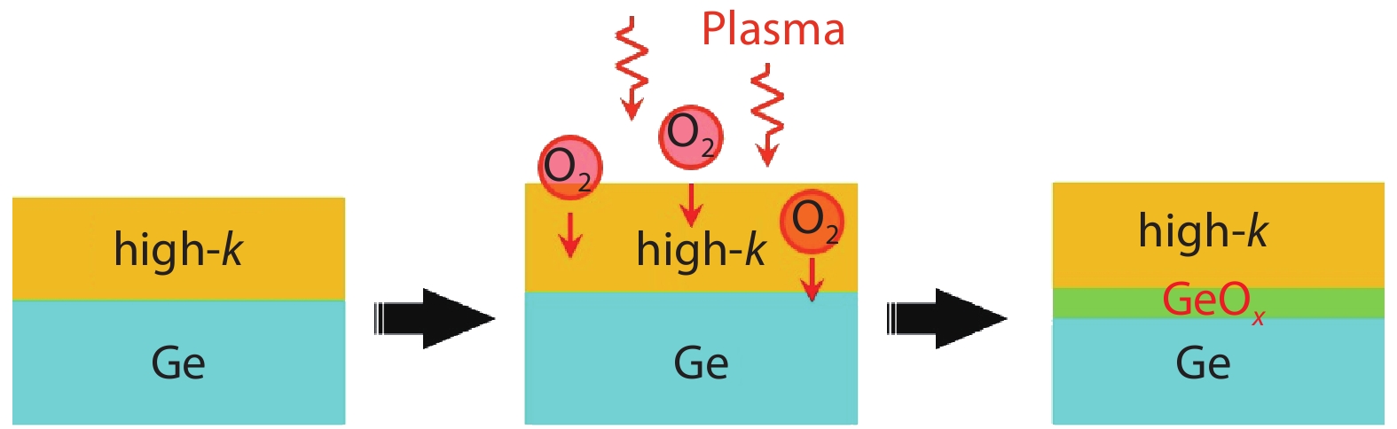
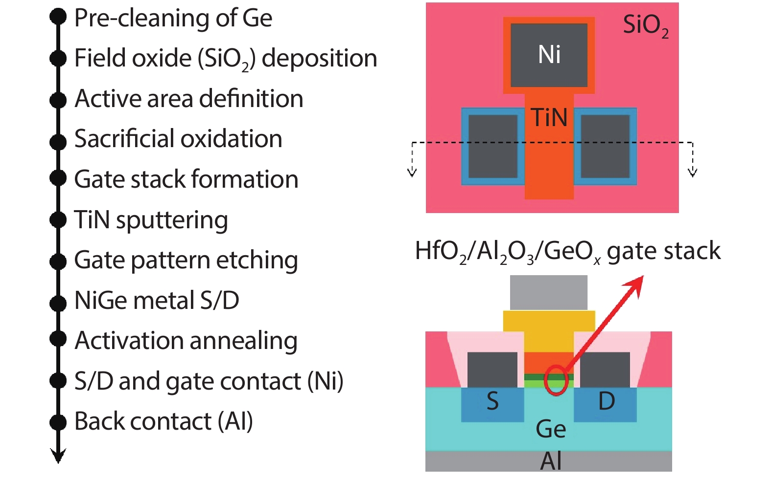
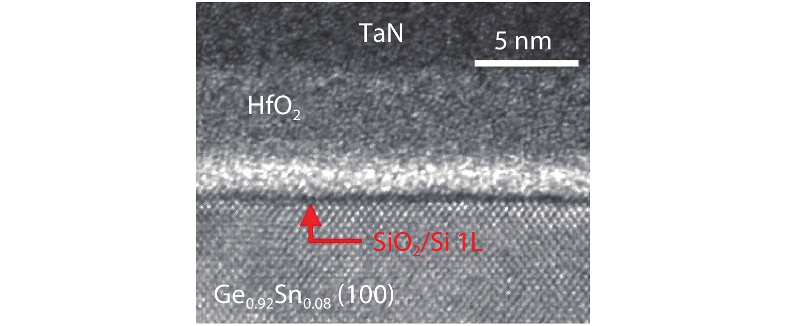
Fig. 1.
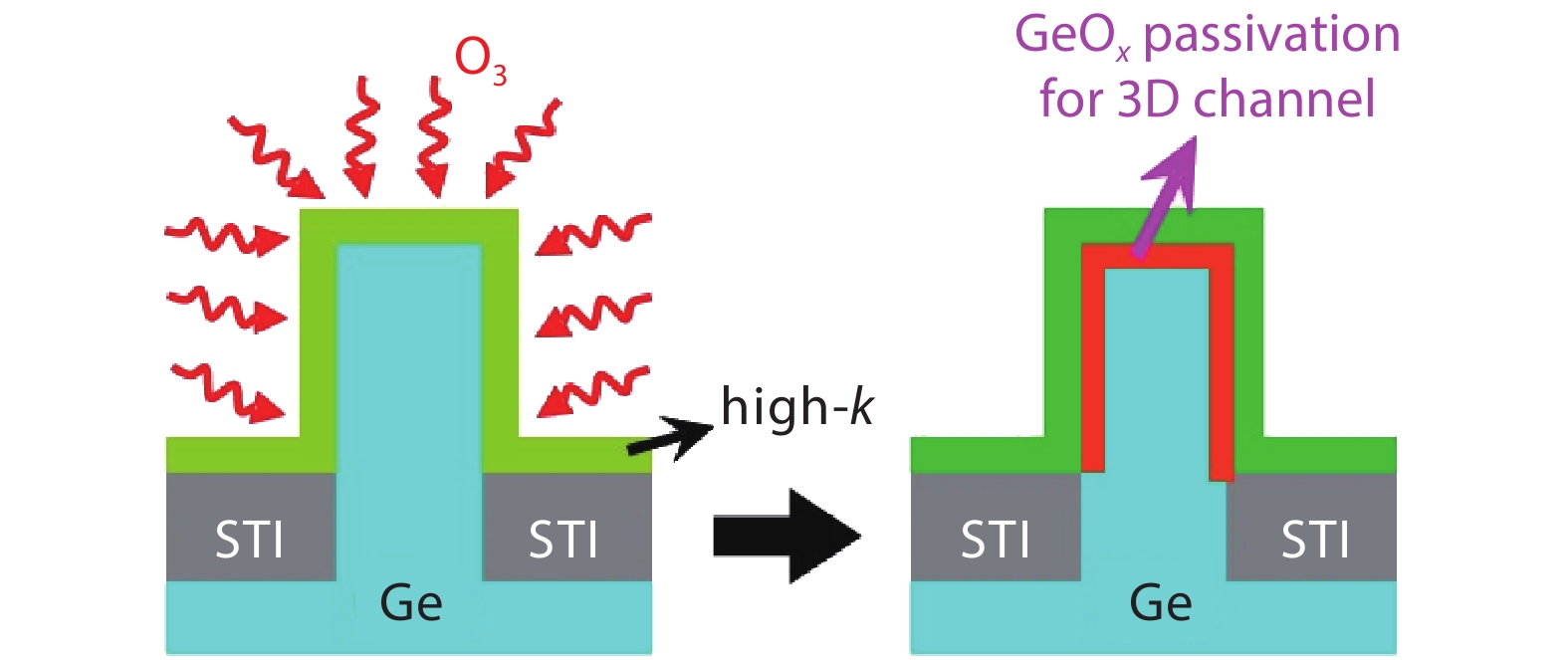
(Color online) The fabrication process of the high-k/GeOx/Ge gate stacks with PPO method.
REVIEWS
Ran Cheng1, Zhuo Chen1, Sicong Yuan1, Mitsuru Takenaka3, Shinichi Takagi3, Genquan Han2 and Rui Zhang1,
Corresponding author: Rui Zhang, ruizhang@zju.edu.cn
Abstract: The performance enhancement of conventional Si MOSFETs through device scaling is becoming increasingly difficult. The application of high mobility channel materials is one of the most promising solutions to overcome the bottleneck. The Ge and GeSn channels attract a lot of interest as the alternative channel materials, not only because of the high carrier mobility but also the superior compatibility with typical Si CMOS technology. In this paper, the recent progress of high mobility Ge and GeSn MOSFETs has been investigated, providing feasible approaches to improve the performance of Ge and GeSn devices for future CMOS technologies.
Keywords: germanium, germanium-tin, MOSFET, mobility
| [1] |
Kuhn K. Considerations for ultimate CMOS scaling. IEEE Trans Electron Devices, 2012, 59(7), 1813 doi: 10.1109/TED.2012.2193129
|
| [2] |
Auth C, Aliyarukunju A, Asoro M, et al. A 10 nm high performance and low-power CMOS technology featuring 3rd generation FinFET transistors, self-aligned quad patterning, contact over active gate and cobalt local interconnects. IEDM Tech Dig, 2017, 29.1 doi: 10.1109/IEDM.2017.8268472
|
| [3] |
Narasimha S, Jagannathan B, Ogino A, et al. A 7 nm CMOS technology platform for mobile and high performance compute application. IEDM Tech Dig, 2017, 29.5 doi: 10.1109/IEDM.2017.8268476
|
| [4] |
International Roadmap of Devices and Systems (IRDS), 2020 edition. https://irds.ieee.org/editions/2020
|
| [5] |
Rim K, Welser J, Hoyt J L, et al. Enhanced hole mobilities in surface-channel strained-Si p-MOSFETs. IEDM Tech Dig, 1995, 517 doi: 10.1109/IEDM.1995.499251
|
| [6] |
Takagi S, Hoyt J L, Welser J J, et al. Comparative study of phonon-limited mobility of two-dimensional electrons in strained and unstrained Si metal–oxide–semiconductor field-effect transistors. J Appl Phys, 1996, 80(3), 1567 doi: 10.1063/1.362953
|
| [7] |
Takagi S, Mizuno T, Tezuka T, et al. Channel structure design, fabrication and carrier transport properties of strained-Si/SiGe-on-insulator (strained-SOI) MOSFETs. IEDM Tech Dig, 2003, 57 doi: 10.1109/IEDM.2003.1269165
|
| [8] |
Shang H, Frank M M, Gusev E P, et al. Germanium channel MOSFETs: Opportunities and challenges. IBM J Res Dev, 2006, 50(4/5), 377 doi: 10.1147/rd.504.0377
|
| [9] |
Saraswat K C, Chui C O, Krishnamohan T, et al. Ge based high performance nanoscale MOSFETs. Microelectron Eng, 2005, 80(6), 15 doi: 10.1016/j.mee.2005.04.038
|
| [10] |
Gupta S, Chen R, Magyari-Kope B, et al. GeSn technology: Extending the Ge electronics roadmap. IEEE Tech Dig, 2011, 16.6 doi: 10.1109/IEDM.2011.6131568
|
| [11] |
Gong X, Han G Q, Bai F, et al. Germanium-tin (GeSn) p-channel MOSFETs fabricated on (100) and (111) surface orientations with sub-400 oC Si2H6 passivation. IEEE Electron Device Lett, 2013, 34(3), 339 doi: 10.1109/LED.2012.2236880
|
| [12] |
Lieten R R, Maeda T, Jevasuwan W, et al. Tensile-strained GeSn metal-oxide-semiconductor field-effect transistor devices on Si (111) using solid phase epitaxy. Appl Phys Exp, 2013, 6(10), 101301 doi: 10.7567/apex.6.101301
|
| [13] |
Xie R, Phung T H, He W, et al. High mobility high-k/Ge pMOSFETs with 1 nm EOT – New concept on interface engineering and interface characterization. IEDM Tech Dig, 2008, 393 doi: 10.1109/IEDM.2008.4796703
|
| [14] |
Mitard J, Shea C, DeJaeger B, et al. Impact of EOT scaling down to 0.85 nm on 70 nm Ge-pFETs technology with STI. VLSI Symp Tech Dig, 2009, 82
|
| [15] |
Kamata Y, Ikeda K, Kamimuta Y, et al. High-k/Ge p- & n-MISFETs with strontium germanide interlayer for EOT scalable CMIS application. VLSI Symp Tech Dig, 2009, 211 doi: 10.1109/VLSIT.2010.5556231
|
| [16] |
Gupta S, Vincent B, Yang B, et al. Towards high mobility GeSn channel nMOSFETs: Improved surface passivation using novel ozone oxidation method. IEDM Tech Dig, 2012, 16.2 doi: 10.1109/IEDM.2012.6479052
|
| [17] |
Liu L, Liang R R, Wang J, et al. Hole mobility enhancement of GeSn/Ge pMOSFETs with an interlayer formed by Sn-assisted oxynitridation. ECS Solid State Lett, 2014, 3(11), Q76 doi: 10.1149/2.0071411ssl
|
| [18] |
Haffner T, Mahjoub M A, Labau S, et al. Improvement of the electrical performance of Au/Ti/HfO2/Ge0.9Sn0.1 p-MOS capacitors by using interfacial layers. Appl Phys Lett, 2019, 115(17), 171601 doi: 10.1063/1.5121474
|
| [19] |
Nakakita Y, Nakane R, Sasada T, et al. Interface-controlled self-align source/drain Ge p-channel metal-oxide-semiconductor field-effect transistors fabricated using thermally oxidized GeO2 interfacial layers. Jpn J Appl Phys, 2011, 50(1), 010109 doi: 10.1109/IEDM.2008.4796838
|
| [20] |
Morii K, Iwasaki T, Nakane R, et al. High performance GeO2/Ge nMOSFETs with source/drain junctions formed by gas phase doping. IEEE Electron Device Lett, 2010, 31(10), 1092 doi: 10.1109/LED.2010.2061211
|
| [21] |
Lee C H, Nishimura T, Tabata T, et al. Ge MOSFETs performance: Impact of Ge interface passivation. IEDM Tech Dig, 2010, 416 doi: 10.1109/IEDM.2010.5703384
|
| [22] |
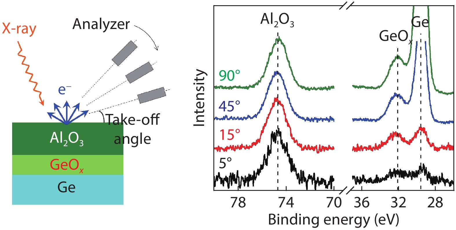
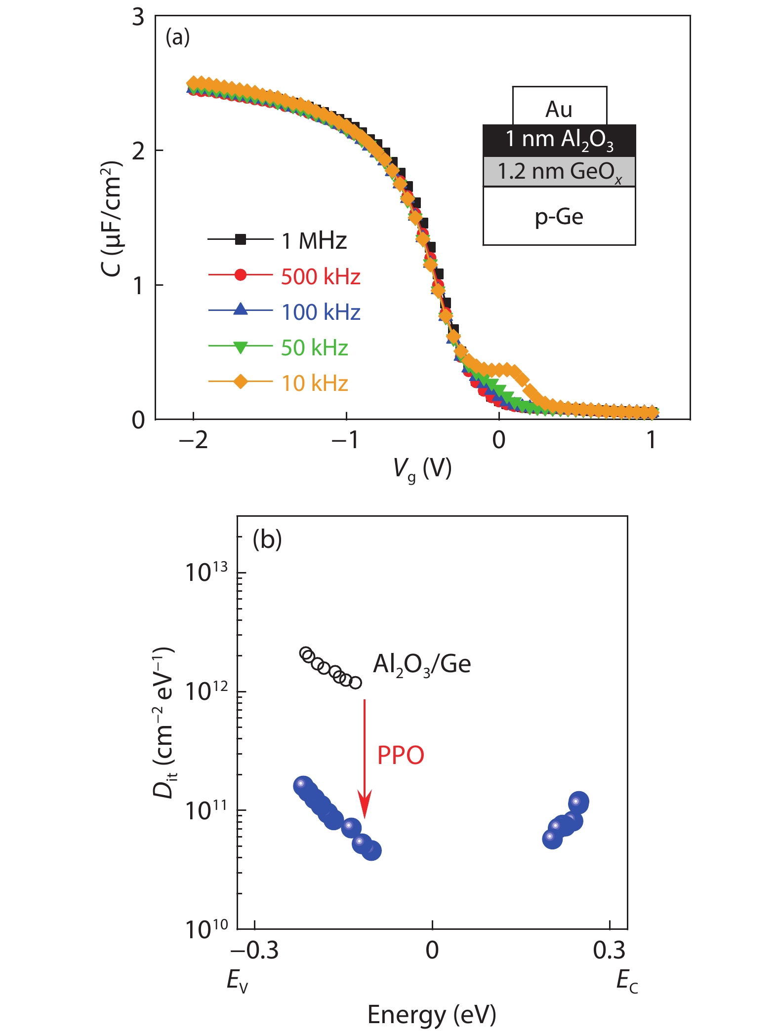
Zhang R, Iwasaki T, Taoka N, et al. Al2O3/GeOx/Ge gate stacks with low interface trap density fabricated by electron cyclotron resonance plasma postoxidation. Appl Phys Lett, 2011, 98(11), 112902 doi: 10.1063/1.3564902
|
| [23] |
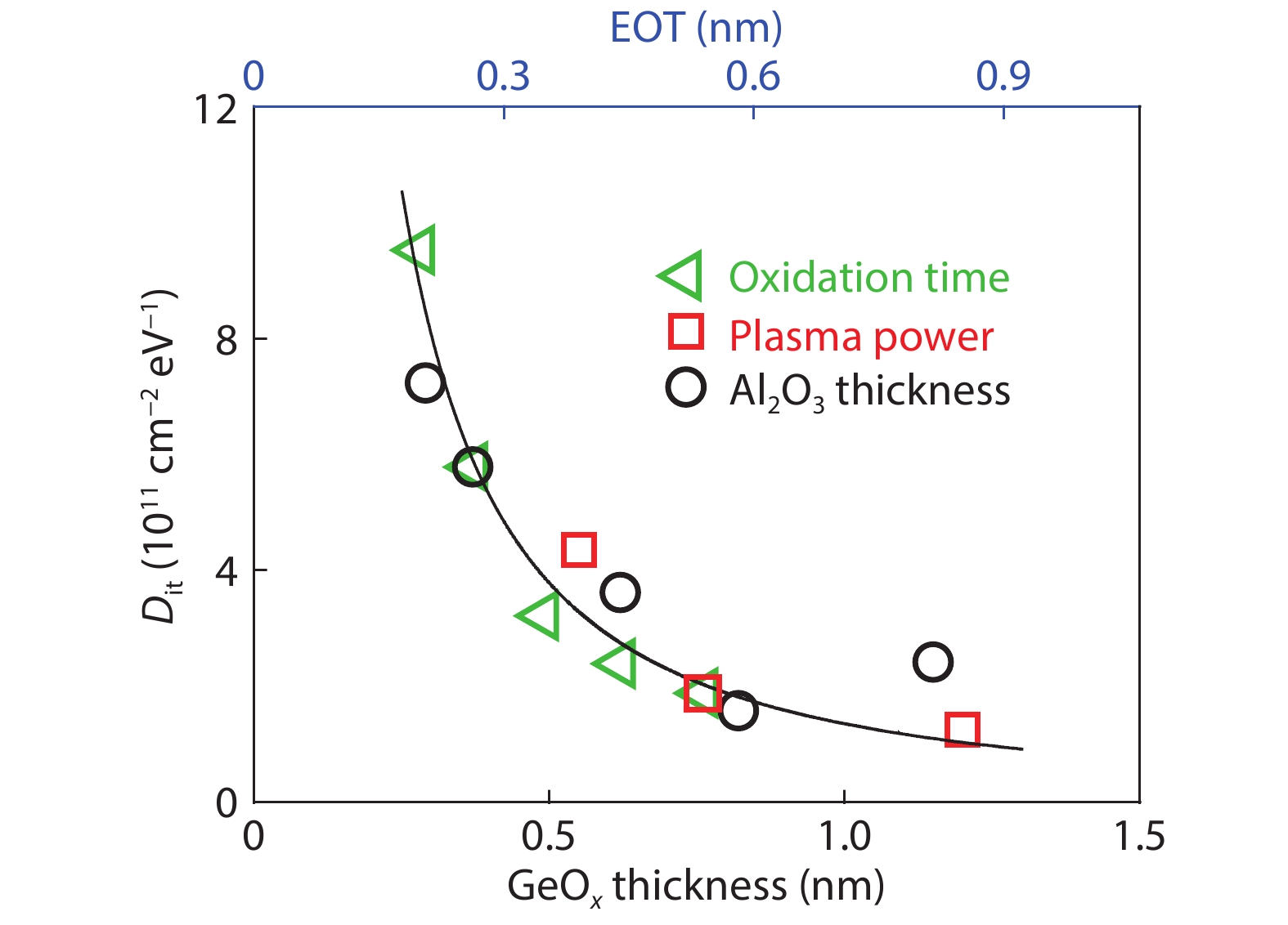
Zhang R, Iwasaki T, Taoka N, et al. Impact of GeOx interfacial layer thickness on Al2O3/Ge MOS interface properties. Microelectron Eng, 2011, 88(7), 1533 doi: 10.1016/j.mee.2011.03.130
|
| [24] |
Zhang R, Iwasaki T, Taoka N, et al. High-mobility Ge pMOSFET with 1-nm-thick EOT Al2O3/GeOx/Ge gate stack fabricated by plasma post oxidation. IEEE Trans Electron Devices, 2012, 59(2), 335 doi: 10.1109/TED.2011.2176495
|
| [25] |
Zhang R, Huang P C, Lin J C, et al. High-mobility Ge p- and n-MOSFET with 0.7-nm EOT using HfO2/Al2O3/GeOx/Ge gate stacks fabricated by plasma postoxidation. IEEE Trans Electron Devices, 2013, 60(3), 927 doi: 10.1109/TED.2013.2238942
|
| [26] |
Taoka N, Ikeda K, Yamashita Y, et al. Quantitative evaluation of interface trap density in Ge-MIS interfaces. Ext Abst SSDM, 2006, 396 doi: 10.7567/SSDM.2006.J-6-1
|
| [27] |
Matsubara H, Kumagai H, Sugahara S, et al. Evaluation of SiO2/GeO2/Ge MIS interface properties by low temperature conductance method. Ext Abst SSDM, 2007, 18 doi: 10.7567/SSDM.2007.A-2-1
|
| [28] |
Martens K, Jaeger B D, Bonzom R, et al. New interface state density extraction method applicable to peaked and high-density distributions for Ge MOSFET development. IEEE Electron Device Lett, 2006, 27(5), 405 doi: 10.1109/LED.2006.873767
|
| [29] |
Brews J R. Rapid interface parameterization using a single MOS conductance curve. Solid-State Electron, 1983, 26(8), 711 doi: 10.1016/0038-1101(83)90030-8
|
| [30] |
Smith G S, Isaacs P B. The crystal structure of quartz-like GeO2. Acta Cryst, 1964, 17(7), 842 doi: 10.1107/S0365110X64002262
|
| [31] |
Van Elshocht S, Caymax M, Conard T, et al. Effect of hafnium germinate formation on the interface of HfO2/germanium metal oxide semiconductor devices. Appl Phys Lett, 2006, 88(14), 141904 doi: 10.1063/1.2192576
|
| [32] |
Houssa M, Pourtois G, Caymax M, et al. First-principles study of the structural and electronic properties of (100) Ge/Ge(M)O2 interfaces (M = Al, La, or Hf). Appl Phys Lett, 2008, 92(24), 242101 doi: 10.1016/j.jeurceramsoc.2007.12.036
|
| [33] |
Migita S, Watanabe Y, Ota H, et al. Design and demonstration of very high-k (k similar to 50) HfO2 for ultra-scaled Si CMOS. VLSI Symp Tech Dig, 2008, 119 doi: 10.1109/VLSIT.2008.4588599
|
| [34] |
Tsipas P, Volkos S N, Sotiropoulos A, et al. Germanium-induced stabilization of a very high-k zirconia phase in ZrO2/GeO2 gate stacks. Appl Phys Lett, 2008, 93(8), 082904 doi: 10.1063/1.2977555
|
| [35] |
Tsoutsou D, Apostolopoulos G, Galata S, et al. Stabilization of a very high-k tetragonal ZrO2 phase by direct doping with germanium. Microelectron Eng, 2009, 86(7–9), 1626 doi: 10.1016/j.mee.2009.02.037
|
| [36] |
Oshima Y, Shandalov M, Sun Y, et al. Hafnium oxide/germanium oxynitride gate stacks on germanium: Capacitance scaling and interface state density. Appl Phys Lett, 2009, 94(18), 183102 doi: 10.1063/1.3116624
|
| [37] |
Fu C H, Chang-Liao K S, Liu L J, et al. An ultralow EOT Ge MOS device with tetragonal HfO2 and high quality HfxGeyO interfacial layer. IEEE Trans Electron Devices, 2014, 61(8), 2662 doi: 10.1109/TED.2014.2329839
|
| [38] |
Han G, Su S, Zhan C, Zhou Q, et al. High-mobility germanium-tin (GeSn) p-channel MOSFETs featuring metallic source/drain and sub-370 oC process modules. IEDM Tech Dig, 2011, 402 doi: 10.1109/IEDM.2011.6131569
|
| [39] |
Gupta S, Huang Y C, Kim Y, et al. Hole enhancement in compressively strained Ge0.93Sn0.07 pMOSFETs. IEEE Electron Device Lett, 2013, 34(7), 58 doi: 10.1109/LED.2013.2259573
|
| [40] |
Liu M, Han G, Liu Y, et al. Undoped Ge0.92Sn0.08 quantum well pMOSFETs on (001), (011) and (111) substrates with in situ Si2H6 passivation: High hole mobility and dependence of performance on orientation. VLSI Symp Tech Dig, 2014, 100 doi: 10.1109/VLSIT.2014.6894376
|
| [41] |
Mizuno T, Takagi S, Sugiyama N, et al. Electron and hole mobility enhancement in strained-Si MOSFET's on SiGe-on-insulator substrates fabricated by SIMOX technology. IEEE Electron Device Lett, 2000, 21(5), 230 doi: 10.1109/55.841305
|
| [42] |
Thompson S E, Armstrong M, Auth C, et al. A 90-nm logic technology featuring strained-silicon. IEEE Trans Electron Device, 2004, 51(11), 1790 doi: 10.1109/TED.2004.836648
|
| [43] |
Lee M L, Fitzgerald E A, Bulsara M T, et al. Strained Si, and Ge channels for high-mobility metal –oxide –semiconductor field-effect transistors. J Appl Phys, 2005, 97(1), 011101 doi: 10.1063/1.1819976
|
| [44] |
Nakaharai S, Tezuka T, Sugiyama N, et al. Characterization of 7-nm-thick strained Ge-on-insulator layer fabricated by Ge-condensation technique. Appl Phys Phys, 2003, 83(17), 3516 doi: 10.1063/1.1622442
|
| [45] |
Krishnamohan T, Krivokapic Z, Uchida K, et al. High-mobility ultrathin strained Ge MOSFETs on bulk and SOI with low band-to-band tunneling leakage: Experiments. IEEE Trans Electron Devices, 2006, 53(5), 990 doi: 10.1109/ted.2006.872362
|
| [46] |
Gupta S, Magyari-Kope B, Nishi Y, et al. Achieving direct band gap in germanium through integration of Sn alloying and external strain. J Appl Phys, 2014, 113(7), 073707 doi: 10.1063/1.4792649
|
| [47] |
Yang Y, Low K L, Wang W, et al. Germanium-tin n-channel tunneling field-effect transistor: Device physics and simulation study. J Appl Phys, 2013, 113(19), 194507 doi: 10.1063/1.4805051
|
| [1] |
Kuhn K. Considerations for ultimate CMOS scaling. IEEE Trans Electron Devices, 2012, 59(7), 1813 doi: 10.1109/TED.2012.2193129
|
| [2] |
Auth C, Aliyarukunju A, Asoro M, et al. A 10 nm high performance and low-power CMOS technology featuring 3rd generation FinFET transistors, self-aligned quad patterning, contact over active gate and cobalt local interconnects. IEDM Tech Dig, 2017, 29.1 doi: 10.1109/IEDM.2017.8268472
|
| [3] |
Narasimha S, Jagannathan B, Ogino A, et al. A 7 nm CMOS technology platform for mobile and high performance compute application. IEDM Tech Dig, 2017, 29.5 doi: 10.1109/IEDM.2017.8268476
|
| [4] |
International Roadmap of Devices and Systems (IRDS), 2020 edition. https://irds.ieee.org/editions/2020
|
| [5] |
Rim K, Welser J, Hoyt J L, et al. Enhanced hole mobilities in surface-channel strained-Si p-MOSFETs. IEDM Tech Dig, 1995, 517 doi: 10.1109/IEDM.1995.499251
|
| [6] |
Takagi S, Hoyt J L, Welser J J, et al. Comparative study of phonon-limited mobility of two-dimensional electrons in strained and unstrained Si metal–oxide–semiconductor field-effect transistors. J Appl Phys, 1996, 80(3), 1567 doi: 10.1063/1.362953
|
| [7] |
Takagi S, Mizuno T, Tezuka T, et al. Channel structure design, fabrication and carrier transport properties of strained-Si/SiGe-on-insulator (strained-SOI) MOSFETs. IEDM Tech Dig, 2003, 57 doi: 10.1109/IEDM.2003.1269165
|
| [8] |
Shang H, Frank M M, Gusev E P, et al. Germanium channel MOSFETs: Opportunities and challenges. IBM J Res Dev, 2006, 50(4/5), 377 doi: 10.1147/rd.504.0377
|
| [9] |
Saraswat K C, Chui C O, Krishnamohan T, et al. Ge based high performance nanoscale MOSFETs. Microelectron Eng, 2005, 80(6), 15 doi: 10.1016/j.mee.2005.04.038
|
| [10] |
Gupta S, Chen R, Magyari-Kope B, et al. GeSn technology: Extending the Ge electronics roadmap. IEEE Tech Dig, 2011, 16.6 doi: 10.1109/IEDM.2011.6131568
|
| [11] |
Gong X, Han G Q, Bai F, et al. Germanium-tin (GeSn) p-channel MOSFETs fabricated on (100) and (111) surface orientations with sub-400 oC Si2H6 passivation. IEEE Electron Device Lett, 2013, 34(3), 339 doi: 10.1109/LED.2012.2236880
|
| [12] |
Lieten R R, Maeda T, Jevasuwan W, et al. Tensile-strained GeSn metal-oxide-semiconductor field-effect transistor devices on Si (111) using solid phase epitaxy. Appl Phys Exp, 2013, 6(10), 101301 doi: 10.7567/apex.6.101301
|
| [13] |
Xie R, Phung T H, He W, et al. High mobility high-k/Ge pMOSFETs with 1 nm EOT – New concept on interface engineering and interface characterization. IEDM Tech Dig, 2008, 393 doi: 10.1109/IEDM.2008.4796703
|
| [14] |
Mitard J, Shea C, DeJaeger B, et al. Impact of EOT scaling down to 0.85 nm on 70 nm Ge-pFETs technology with STI. VLSI Symp Tech Dig, 2009, 82
|
| [15] |
Kamata Y, Ikeda K, Kamimuta Y, et al. High-k/Ge p- & n-MISFETs with strontium germanide interlayer for EOT scalable CMIS application. VLSI Symp Tech Dig, 2009, 211 doi: 10.1109/VLSIT.2010.5556231
|
| [16] |
Gupta S, Vincent B, Yang B, et al. Towards high mobility GeSn channel nMOSFETs: Improved surface passivation using novel ozone oxidation method. IEDM Tech Dig, 2012, 16.2 doi: 10.1109/IEDM.2012.6479052
|
| [17] |
Liu L, Liang R R, Wang J, et al. Hole mobility enhancement of GeSn/Ge pMOSFETs with an interlayer formed by Sn-assisted oxynitridation. ECS Solid State Lett, 2014, 3(11), Q76 doi: 10.1149/2.0071411ssl
|
| [18] |
Haffner T, Mahjoub M A, Labau S, et al. Improvement of the electrical performance of Au/Ti/HfO2/Ge0.9Sn0.1 p-MOS capacitors by using interfacial layers. Appl Phys Lett, 2019, 115(17), 171601 doi: 10.1063/1.5121474
|
| [19] |
Nakakita Y, Nakane R, Sasada T, et al. Interface-controlled self-align source/drain Ge p-channel metal-oxide-semiconductor field-effect transistors fabricated using thermally oxidized GeO2 interfacial layers. Jpn J Appl Phys, 2011, 50(1), 010109 doi: 10.1109/IEDM.2008.4796838
|
| [20] |
Morii K, Iwasaki T, Nakane R, et al. High performance GeO2/Ge nMOSFETs with source/drain junctions formed by gas phase doping. IEEE Electron Device Lett, 2010, 31(10), 1092 doi: 10.1109/LED.2010.2061211
|
| [21] |
Lee C H, Nishimura T, Tabata T, et al. Ge MOSFETs performance: Impact of Ge interface passivation. IEDM Tech Dig, 2010, 416 doi: 10.1109/IEDM.2010.5703384
|
| [22] |
Zhang R, Iwasaki T, Taoka N, et al. Al2O3/GeOx/Ge gate stacks with low interface trap density fabricated by electron cyclotron resonance plasma postoxidation. Appl Phys Lett, 2011, 98(11), 112902 doi: 10.1063/1.3564902
|
| [23] |
Zhang R, Iwasaki T, Taoka N, et al. Impact of GeOx interfacial layer thickness on Al2O3/Ge MOS interface properties. Microelectron Eng, 2011, 88(7), 1533 doi: 10.1016/j.mee.2011.03.130
|
| [24] |
Zhang R, Iwasaki T, Taoka N, et al. High-mobility Ge pMOSFET with 1-nm-thick EOT Al2O3/GeOx/Ge gate stack fabricated by plasma post oxidation. IEEE Trans Electron Devices, 2012, 59(2), 335 doi: 10.1109/TED.2011.2176495
|
| [25] |
Zhang R, Huang P C, Lin J C, et al. High-mobility Ge p- and n-MOSFET with 0.7-nm EOT using HfO2/Al2O3/GeOx/Ge gate stacks fabricated by plasma postoxidation. IEEE Trans Electron Devices, 2013, 60(3), 927 doi: 10.1109/TED.2013.2238942
|
| [26] |
Taoka N, Ikeda K, Yamashita Y, et al. Quantitative evaluation of interface trap density in Ge-MIS interfaces. Ext Abst SSDM, 2006, 396 doi: 10.7567/SSDM.2006.J-6-1
|
| [27] |
Matsubara H, Kumagai H, Sugahara S, et al. Evaluation of SiO2/GeO2/Ge MIS interface properties by low temperature conductance method. Ext Abst SSDM, 2007, 18 doi: 10.7567/SSDM.2007.A-2-1
|
| [28] |
Martens K, Jaeger B D, Bonzom R, et al. New interface state density extraction method applicable to peaked and high-density distributions for Ge MOSFET development. IEEE Electron Device Lett, 2006, 27(5), 405 doi: 10.1109/LED.2006.873767
|
| [29] |
Brews J R. Rapid interface parameterization using a single MOS conductance curve. Solid-State Electron, 1983, 26(8), 711 doi: 10.1016/0038-1101(83)90030-8
|
| [30] |
Smith G S, Isaacs P B. The crystal structure of quartz-like GeO2. Acta Cryst, 1964, 17(7), 842 doi: 10.1107/S0365110X64002262
|
| [31] |
Van Elshocht S, Caymax M, Conard T, et al. Effect of hafnium germinate formation on the interface of HfO2/germanium metal oxide semiconductor devices. Appl Phys Lett, 2006, 88(14), 141904 doi: 10.1063/1.2192576
|
| [32] |
Houssa M, Pourtois G, Caymax M, et al. First-principles study of the structural and electronic properties of (100) Ge/Ge(M)O2 interfaces (M = Al, La, or Hf). Appl Phys Lett, 2008, 92(24), 242101 doi: 10.1016/j.jeurceramsoc.2007.12.036
|
| [33] |
Migita S, Watanabe Y, Ota H, et al. Design and demonstration of very high-k (k similar to 50) HfO2 for ultra-scaled Si CMOS. VLSI Symp Tech Dig, 2008, 119 doi: 10.1109/VLSIT.2008.4588599
|
| [34] |
Tsipas P, Volkos S N, Sotiropoulos A, et al. Germanium-induced stabilization of a very high-k zirconia phase in ZrO2/GeO2 gate stacks. Appl Phys Lett, 2008, 93(8), 082904 doi: 10.1063/1.2977555
|
| [35] |
Tsoutsou D, Apostolopoulos G, Galata S, et al. Stabilization of a very high-k tetragonal ZrO2 phase by direct doping with germanium. Microelectron Eng, 2009, 86(7–9), 1626 doi: 10.1016/j.mee.2009.02.037
|
| [36] |
Oshima Y, Shandalov M, Sun Y, et al. Hafnium oxide/germanium oxynitride gate stacks on germanium: Capacitance scaling and interface state density. Appl Phys Lett, 2009, 94(18), 183102 doi: 10.1063/1.3116624
|
| [37] |
Fu C H, Chang-Liao K S, Liu L J, et al. An ultralow EOT Ge MOS device with tetragonal HfO2 and high quality HfxGeyO interfacial layer. IEEE Trans Electron Devices, 2014, 61(8), 2662 doi: 10.1109/TED.2014.2329839
|
| [38] |
Han G, Su S, Zhan C, Zhou Q, et al. High-mobility germanium-tin (GeSn) p-channel MOSFETs featuring metallic source/drain and sub-370 oC process modules. IEDM Tech Dig, 2011, 402 doi: 10.1109/IEDM.2011.6131569
|
| [39] |
Gupta S, Huang Y C, Kim Y, et al. Hole enhancement in compressively strained Ge0.93Sn0.07 pMOSFETs. IEEE Electron Device Lett, 2013, 34(7), 58 doi: 10.1109/LED.2013.2259573
|
| [40] |
Liu M, Han G, Liu Y, et al. Undoped Ge0.92Sn0.08 quantum well pMOSFETs on (001), (011) and (111) substrates with in situ Si2H6 passivation: High hole mobility and dependence of performance on orientation. VLSI Symp Tech Dig, 2014, 100 doi: 10.1109/VLSIT.2014.6894376
|
| [41] |
Mizuno T, Takagi S, Sugiyama N, et al. Electron and hole mobility enhancement in strained-Si MOSFET's on SiGe-on-insulator substrates fabricated by SIMOX technology. IEEE Electron Device Lett, 2000, 21(5), 230 doi: 10.1109/55.841305
|
| [42] |
Thompson S E, Armstrong M, Auth C, et al. A 90-nm logic technology featuring strained-silicon. IEEE Trans Electron Device, 2004, 51(11), 1790 doi: 10.1109/TED.2004.836648
|
| [43] |
Lee M L, Fitzgerald E A, Bulsara M T, et al. Strained Si, and Ge channels for high-mobility metal –oxide –semiconductor field-effect transistors. J Appl Phys, 2005, 97(1), 011101 doi: 10.1063/1.1819976
|
| [44] |
Nakaharai S, Tezuka T, Sugiyama N, et al. Characterization of 7-nm-thick strained Ge-on-insulator layer fabricated by Ge-condensation technique. Appl Phys Phys, 2003, 83(17), 3516 doi: 10.1063/1.1622442
|
| [45] |
Krishnamohan T, Krivokapic Z, Uchida K, et al. High-mobility ultrathin strained Ge MOSFETs on bulk and SOI with low band-to-band tunneling leakage: Experiments. IEEE Trans Electron Devices, 2006, 53(5), 990 doi: 10.1109/ted.2006.872362
|
| [46] |
Gupta S, Magyari-Kope B, Nishi Y, et al. Achieving direct band gap in germanium through integration of Sn alloying and external strain. J Appl Phys, 2014, 113(7), 073707 doi: 10.1063/1.4792649
|
| [47] |
Yang Y, Low K L, Wang W, et al. Germanium-tin n-channel tunneling field-effect transistor: Device physics and simulation study. J Appl Phys, 2013, 113(19), 194507 doi: 10.1063/1.4805051
|


Article views: 7141 Times PDF downloads: 327 Times Cited by: 0 Times
Received: 22 September 2020 Revised: 02 December 2020 Online: Accepted Manuscript: 16 December 2020Uncorrected proof: 17 December 2020Published: 08 February 2021
| Citation: |
Ran Cheng, Zhuo Chen, Sicong Yuan, Mitsuru Takenaka, Shinichi Takagi, Genquan Han, Rui Zhang. Mobility enhancement techniques for Ge and GeSn MOSFETs[J]. Journal of Semiconductors, 2021, 42(2): 023101. doi: 10.1088/1674-4926/42/2/023101
****
R Cheng, Z Chen, S C Yuan, M Takenaka, S Takagi, G Q Han, R Zhang, Mobility enhancement techniques for Ge and GeSn MOSFETs[J]. J. Semicond., 2021, 42(2): 023101. doi: 10.1088/1674-4926/42/2/023101.

|
| [1] |
Kuhn K. Considerations for ultimate CMOS scaling. IEEE Trans Electron Devices, 2012, 59(7), 1813 doi: 10.1109/TED.2012.2193129
|
| [2] |
Auth C, Aliyarukunju A, Asoro M, et al. A 10 nm high performance and low-power CMOS technology featuring 3rd generation FinFET transistors, self-aligned quad patterning, contact over active gate and cobalt local interconnects. IEDM Tech Dig, 2017, 29.1 doi: 10.1109/IEDM.2017.8268472
|
| [3] |
Narasimha S, Jagannathan B, Ogino A, et al. A 7 nm CMOS technology platform for mobile and high performance compute application. IEDM Tech Dig, 2017, 29.5 doi: 10.1109/IEDM.2017.8268476
|
| [4] |
International Roadmap of Devices and Systems (IRDS), 2020 edition. https://irds.ieee.org/editions/2020
|
| [5] |
Rim K, Welser J, Hoyt J L, et al. Enhanced hole mobilities in surface-channel strained-Si p-MOSFETs. IEDM Tech Dig, 1995, 517 doi: 10.1109/IEDM.1995.499251
|
| [6] |
Takagi S, Hoyt J L, Welser J J, et al. Comparative study of phonon-limited mobility of two-dimensional electrons in strained and unstrained Si metal–oxide–semiconductor field-effect transistors. J Appl Phys, 1996, 80(3), 1567 doi: 10.1063/1.362953
|
| [7] |
Takagi S, Mizuno T, Tezuka T, et al. Channel structure design, fabrication and carrier transport properties of strained-Si/SiGe-on-insulator (strained-SOI) MOSFETs. IEDM Tech Dig, 2003, 57 doi: 10.1109/IEDM.2003.1269165
|
| [8] |
Shang H, Frank M M, Gusev E P, et al. Germanium channel MOSFETs: Opportunities and challenges. IBM J Res Dev, 2006, 50(4/5), 377 doi: 10.1147/rd.504.0377
|
| [9] |
Saraswat K C, Chui C O, Krishnamohan T, et al. Ge based high performance nanoscale MOSFETs. Microelectron Eng, 2005, 80(6), 15 doi: 10.1016/j.mee.2005.04.038
|
| [10] |
Gupta S, Chen R, Magyari-Kope B, et al. GeSn technology: Extending the Ge electronics roadmap. IEEE Tech Dig, 2011, 16.6 doi: 10.1109/IEDM.2011.6131568
|
| [11] |
Gong X, Han G Q, Bai F, et al. Germanium-tin (GeSn) p-channel MOSFETs fabricated on (100) and (111) surface orientations with sub-400 oC Si2H6 passivation. IEEE Electron Device Lett, 2013, 34(3), 339 doi: 10.1109/LED.2012.2236880
|
| [12] |
Lieten R R, Maeda T, Jevasuwan W, et al. Tensile-strained GeSn metal-oxide-semiconductor field-effect transistor devices on Si (111) using solid phase epitaxy. Appl Phys Exp, 2013, 6(10), 101301 doi: 10.7567/apex.6.101301
|
| [13] |
Xie R, Phung T H, He W, et al. High mobility high-k/Ge pMOSFETs with 1 nm EOT – New concept on interface engineering and interface characterization. IEDM Tech Dig, 2008, 393 doi: 10.1109/IEDM.2008.4796703
|
| [14] |
Mitard J, Shea C, DeJaeger B, et al. Impact of EOT scaling down to 0.85 nm on 70 nm Ge-pFETs technology with STI. VLSI Symp Tech Dig, 2009, 82
|
| [15] |
Kamata Y, Ikeda K, Kamimuta Y, et al. High-k/Ge p- & n-MISFETs with strontium germanide interlayer for EOT scalable CMIS application. VLSI Symp Tech Dig, 2009, 211 doi: 10.1109/VLSIT.2010.5556231
|
| [16] |
Gupta S, Vincent B, Yang B, et al. Towards high mobility GeSn channel nMOSFETs: Improved surface passivation using novel ozone oxidation method. IEDM Tech Dig, 2012, 16.2 doi: 10.1109/IEDM.2012.6479052
|
| [17] |
Liu L, Liang R R, Wang J, et al. Hole mobility enhancement of GeSn/Ge pMOSFETs with an interlayer formed by Sn-assisted oxynitridation. ECS Solid State Lett, 2014, 3(11), Q76 doi: 10.1149/2.0071411ssl
|
| [18] |
Haffner T, Mahjoub M A, Labau S, et al. Improvement of the electrical performance of Au/Ti/HfO2/Ge0.9Sn0.1 p-MOS capacitors by using interfacial layers. Appl Phys Lett, 2019, 115(17), 171601 doi: 10.1063/1.5121474
|
| [19] |
Nakakita Y, Nakane R, Sasada T, et al. Interface-controlled self-align source/drain Ge p-channel metal-oxide-semiconductor field-effect transistors fabricated using thermally oxidized GeO2 interfacial layers. Jpn J Appl Phys, 2011, 50(1), 010109 doi: 10.1109/IEDM.2008.4796838
|
| [20] |
Morii K, Iwasaki T, Nakane R, et al. High performance GeO2/Ge nMOSFETs with source/drain junctions formed by gas phase doping. IEEE Electron Device Lett, 2010, 31(10), 1092 doi: 10.1109/LED.2010.2061211
|
| [21] |
Lee C H, Nishimura T, Tabata T, et al. Ge MOSFETs performance: Impact of Ge interface passivation. IEDM Tech Dig, 2010, 416 doi: 10.1109/IEDM.2010.5703384
|
| [22] |
Zhang R, Iwasaki T, Taoka N, et al. Al2O3/GeOx/Ge gate stacks with low interface trap density fabricated by electron cyclotron resonance plasma postoxidation. Appl Phys Lett, 2011, 98(11), 112902 doi: 10.1063/1.3564902
|
| [23] |
Zhang R, Iwasaki T, Taoka N, et al. Impact of GeOx interfacial layer thickness on Al2O3/Ge MOS interface properties. Microelectron Eng, 2011, 88(7), 1533 doi: 10.1016/j.mee.2011.03.130
|
| [24] |
Zhang R, Iwasaki T, Taoka N, et al. High-mobility Ge pMOSFET with 1-nm-thick EOT Al2O3/GeOx/Ge gate stack fabricated by plasma post oxidation. IEEE Trans Electron Devices, 2012, 59(2), 335 doi: 10.1109/TED.2011.2176495
|
| [25] |
Zhang R, Huang P C, Lin J C, et al. High-mobility Ge p- and n-MOSFET with 0.7-nm EOT using HfO2/Al2O3/GeOx/Ge gate stacks fabricated by plasma postoxidation. IEEE Trans Electron Devices, 2013, 60(3), 927 doi: 10.1109/TED.2013.2238942
|
| [26] |
Taoka N, Ikeda K, Yamashita Y, et al. Quantitative evaluation of interface trap density in Ge-MIS interfaces. Ext Abst SSDM, 2006, 396 doi: 10.7567/SSDM.2006.J-6-1
|
| [27] |
Matsubara H, Kumagai H, Sugahara S, et al. Evaluation of SiO2/GeO2/Ge MIS interface properties by low temperature conductance method. Ext Abst SSDM, 2007, 18 doi: 10.7567/SSDM.2007.A-2-1
|
| [28] |
Martens K, Jaeger B D, Bonzom R, et al. New interface state density extraction method applicable to peaked and high-density distributions for Ge MOSFET development. IEEE Electron Device Lett, 2006, 27(5), 405 doi: 10.1109/LED.2006.873767
|
| [29] |
Brews J R. Rapid interface parameterization using a single MOS conductance curve. Solid-State Electron, 1983, 26(8), 711 doi: 10.1016/0038-1101(83)90030-8
|
| [30] |
Smith G S, Isaacs P B. The crystal structure of quartz-like GeO2. Acta Cryst, 1964, 17(7), 842 doi: 10.1107/S0365110X64002262
|
| [31] |
Van Elshocht S, Caymax M, Conard T, et al. Effect of hafnium germinate formation on the interface of HfO2/germanium metal oxide semiconductor devices. Appl Phys Lett, 2006, 88(14), 141904 doi: 10.1063/1.2192576
|
| [32] |
Houssa M, Pourtois G, Caymax M, et al. First-principles study of the structural and electronic properties of (100) Ge/Ge(M)O2 interfaces (M = Al, La, or Hf). Appl Phys Lett, 2008, 92(24), 242101 doi: 10.1016/j.jeurceramsoc.2007.12.036
|
| [33] |
Migita S, Watanabe Y, Ota H, et al. Design and demonstration of very high-k (k similar to 50) HfO2 for ultra-scaled Si CMOS. VLSI Symp Tech Dig, 2008, 119 doi: 10.1109/VLSIT.2008.4588599
|
| [34] |
Tsipas P, Volkos S N, Sotiropoulos A, et al. Germanium-induced stabilization of a very high-k zirconia phase in ZrO2/GeO2 gate stacks. Appl Phys Lett, 2008, 93(8), 082904 doi: 10.1063/1.2977555
|
| [35] |
Tsoutsou D, Apostolopoulos G, Galata S, et al. Stabilization of a very high-k tetragonal ZrO2 phase by direct doping with germanium. Microelectron Eng, 2009, 86(7–9), 1626 doi: 10.1016/j.mee.2009.02.037
|
| [36] |
Oshima Y, Shandalov M, Sun Y, et al. Hafnium oxide/germanium oxynitride gate stacks on germanium: Capacitance scaling and interface state density. Appl Phys Lett, 2009, 94(18), 183102 doi: 10.1063/1.3116624
|
| [37] |
Fu C H, Chang-Liao K S, Liu L J, et al. An ultralow EOT Ge MOS device with tetragonal HfO2 and high quality HfxGeyO interfacial layer. IEEE Trans Electron Devices, 2014, 61(8), 2662 doi: 10.1109/TED.2014.2329839
|
| [38] |
Han G, Su S, Zhan C, Zhou Q, et al. High-mobility germanium-tin (GeSn) p-channel MOSFETs featuring metallic source/drain and sub-370 oC process modules. IEDM Tech Dig, 2011, 402 doi: 10.1109/IEDM.2011.6131569
|
| [39] |
Gupta S, Huang Y C, Kim Y, et al. Hole enhancement in compressively strained Ge0.93Sn0.07 pMOSFETs. IEEE Electron Device Lett, 2013, 34(7), 58 doi: 10.1109/LED.2013.2259573
|
| [40] |
Liu M, Han G, Liu Y, et al. Undoped Ge0.92Sn0.08 quantum well pMOSFETs on (001), (011) and (111) substrates with in situ Si2H6 passivation: High hole mobility and dependence of performance on orientation. VLSI Symp Tech Dig, 2014, 100 doi: 10.1109/VLSIT.2014.6894376
|
| [41] |
Mizuno T, Takagi S, Sugiyama N, et al. Electron and hole mobility enhancement in strained-Si MOSFET's on SiGe-on-insulator substrates fabricated by SIMOX technology. IEEE Electron Device Lett, 2000, 21(5), 230 doi: 10.1109/55.841305
|
| [42] |
Thompson S E, Armstrong M, Auth C, et al. A 90-nm logic technology featuring strained-silicon. IEEE Trans Electron Device, 2004, 51(11), 1790 doi: 10.1109/TED.2004.836648
|
| [43] |
Lee M L, Fitzgerald E A, Bulsara M T, et al. Strained Si, and Ge channels for high-mobility metal –oxide –semiconductor field-effect transistors. J Appl Phys, 2005, 97(1), 011101 doi: 10.1063/1.1819976
|
| [44] |
Nakaharai S, Tezuka T, Sugiyama N, et al. Characterization of 7-nm-thick strained Ge-on-insulator layer fabricated by Ge-condensation technique. Appl Phys Phys, 2003, 83(17), 3516 doi: 10.1063/1.1622442
|
| [45] |
Krishnamohan T, Krivokapic Z, Uchida K, et al. High-mobility ultrathin strained Ge MOSFETs on bulk and SOI with low band-to-band tunneling leakage: Experiments. IEEE Trans Electron Devices, 2006, 53(5), 990 doi: 10.1109/ted.2006.872362
|
| [46] |
Gupta S, Magyari-Kope B, Nishi Y, et al. Achieving direct band gap in germanium through integration of Sn alloying and external strain. J Appl Phys, 2014, 113(7), 073707 doi: 10.1063/1.4792649
|
| [47] |
Yang Y, Low K L, Wang W, et al. Germanium-tin n-channel tunneling field-effect transistor: Device physics and simulation study. J Appl Phys, 2013, 113(19), 194507 doi: 10.1063/1.4805051
|

 WeChat ID
Journal of Semiconductors © 2017 All Rights Reserved 京ICP备05085259号-2

 DownLoad:

