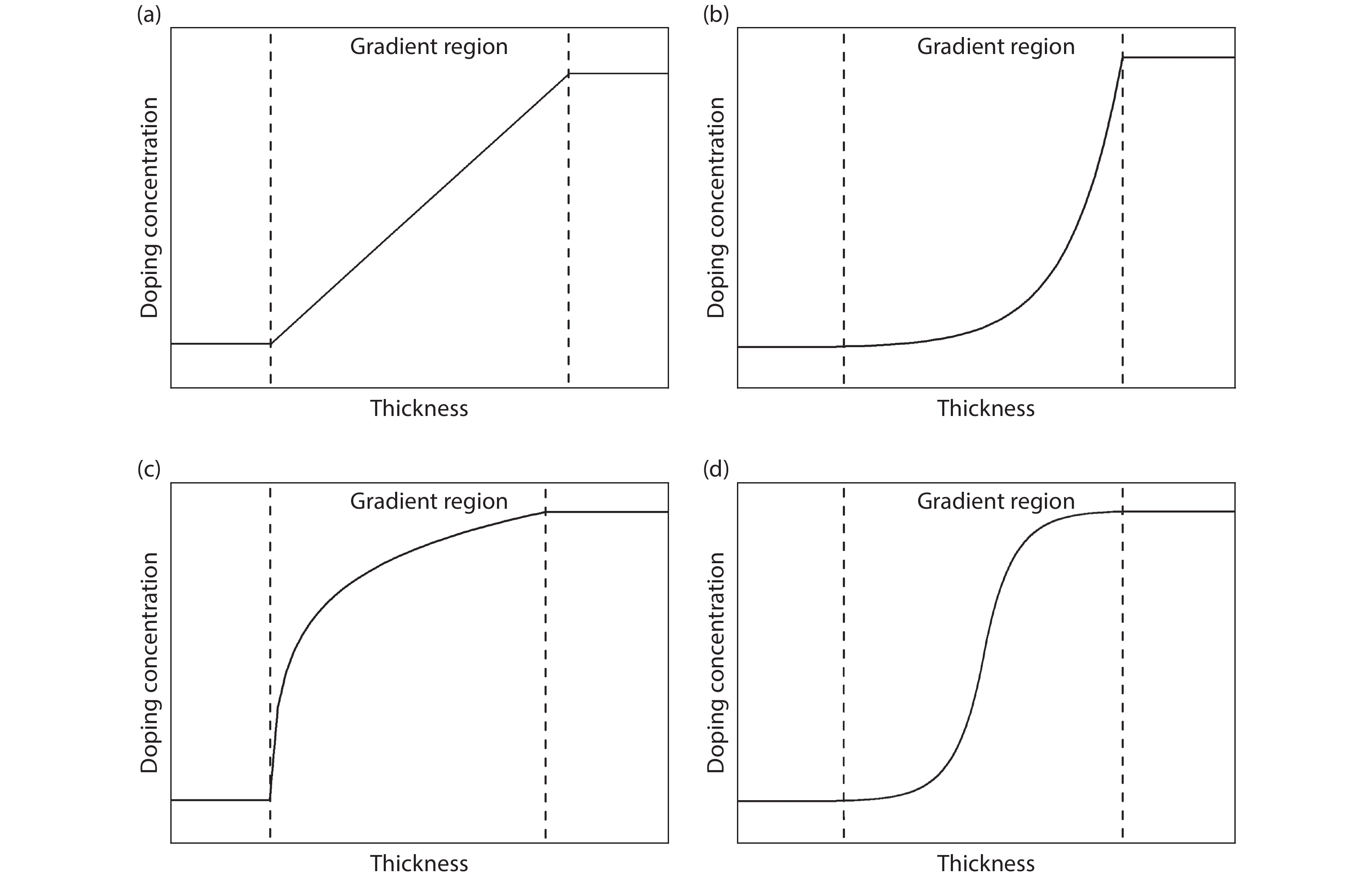
Processing math: 100%
J. Semicond. > 2021, Volume 42 > Issue 3 > 032701

ARTICLES

Energy band adjustment of 808 nm GaAs laser power converters via gradient doping

Yingjie Zhao1, 2, Shan Li1, 2, Huixue Ren1, 2, Shaojie Li1, 2 and Peide Han1, 2,

+ Author Affiliations

 Corresponding author: Peide Han, pdhan@semi.ac.cn

DOI: 10.1088/1674-4926/42/3/032701

PDF

Turn off MathJax

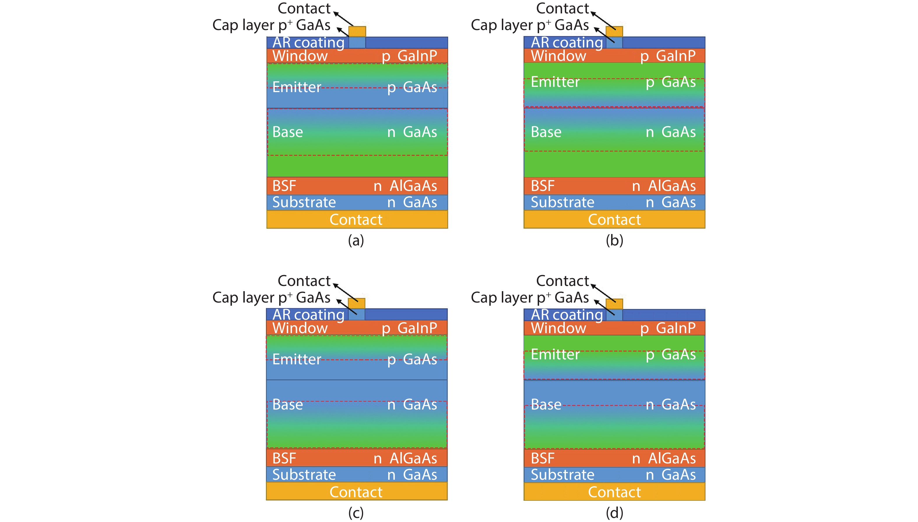
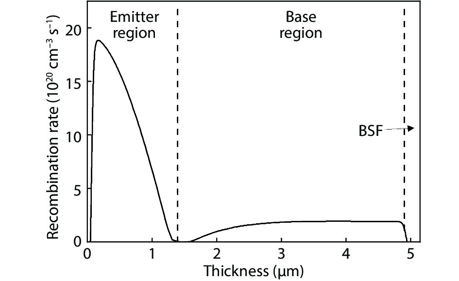
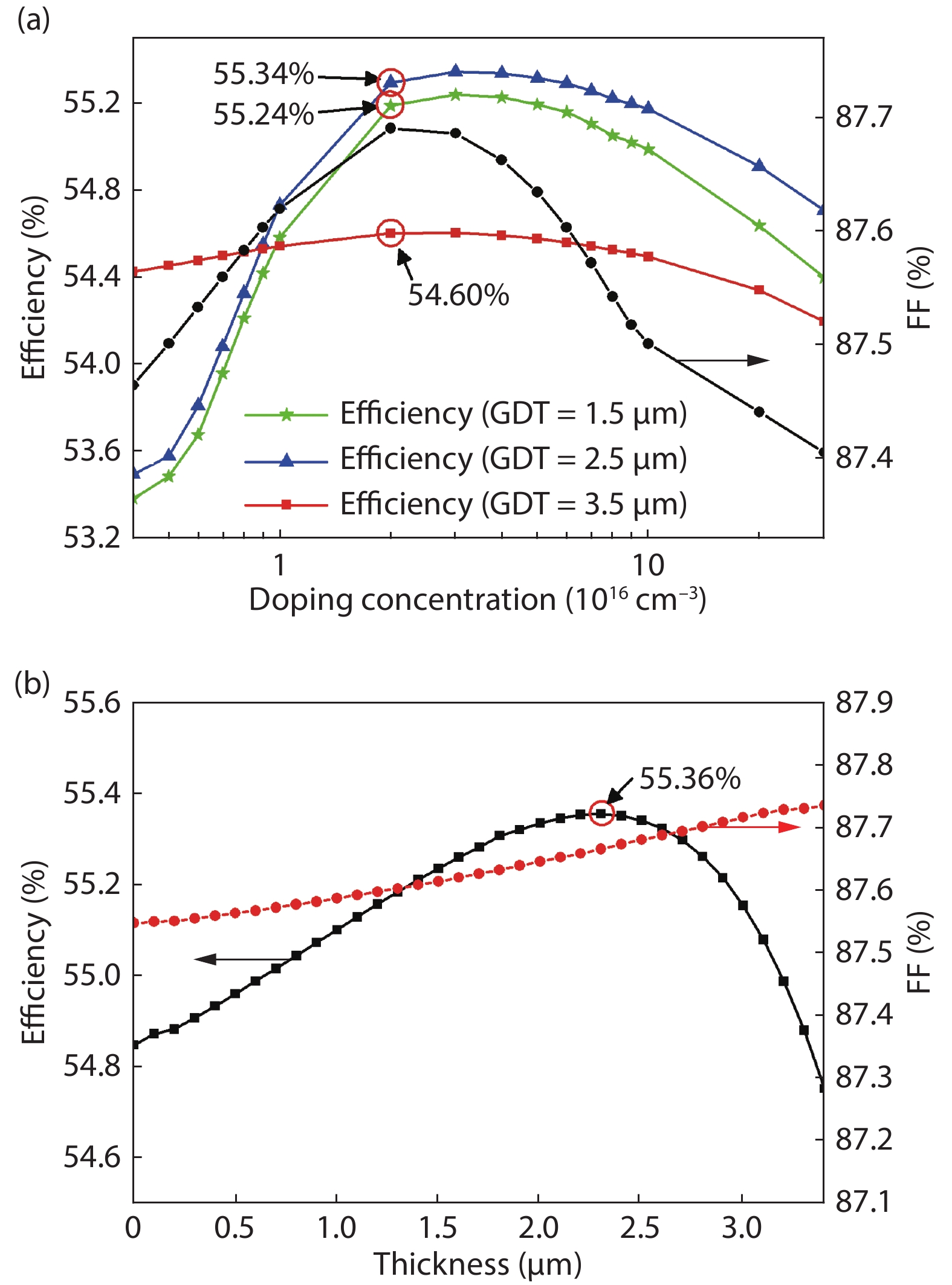
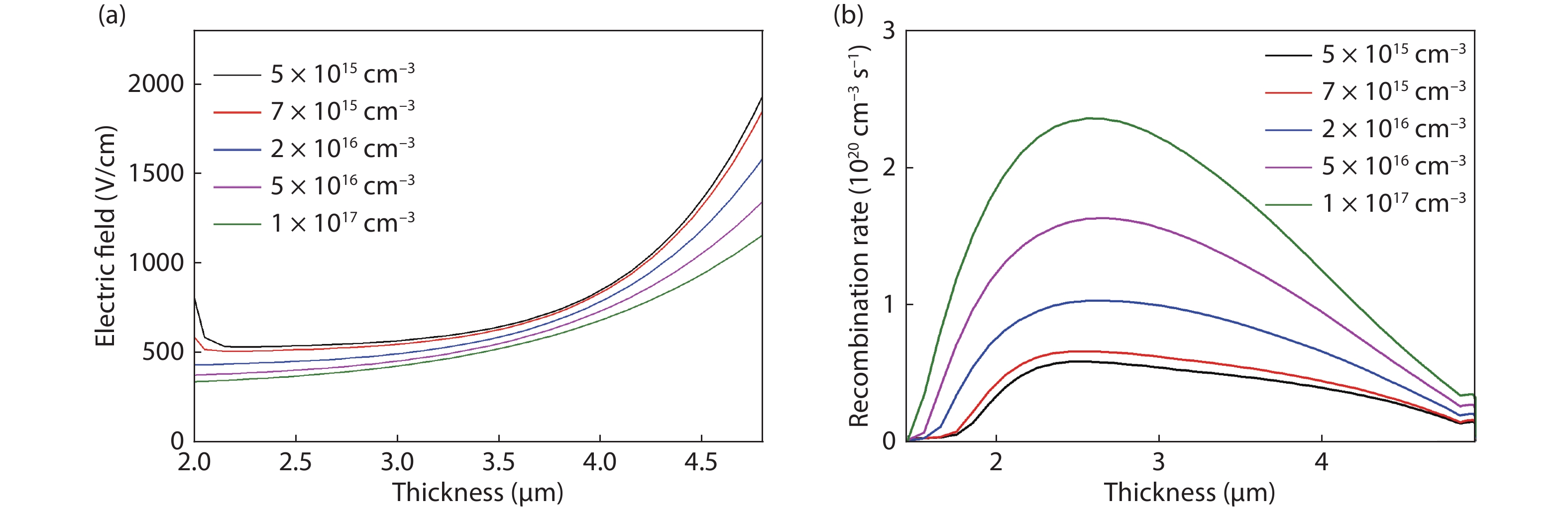
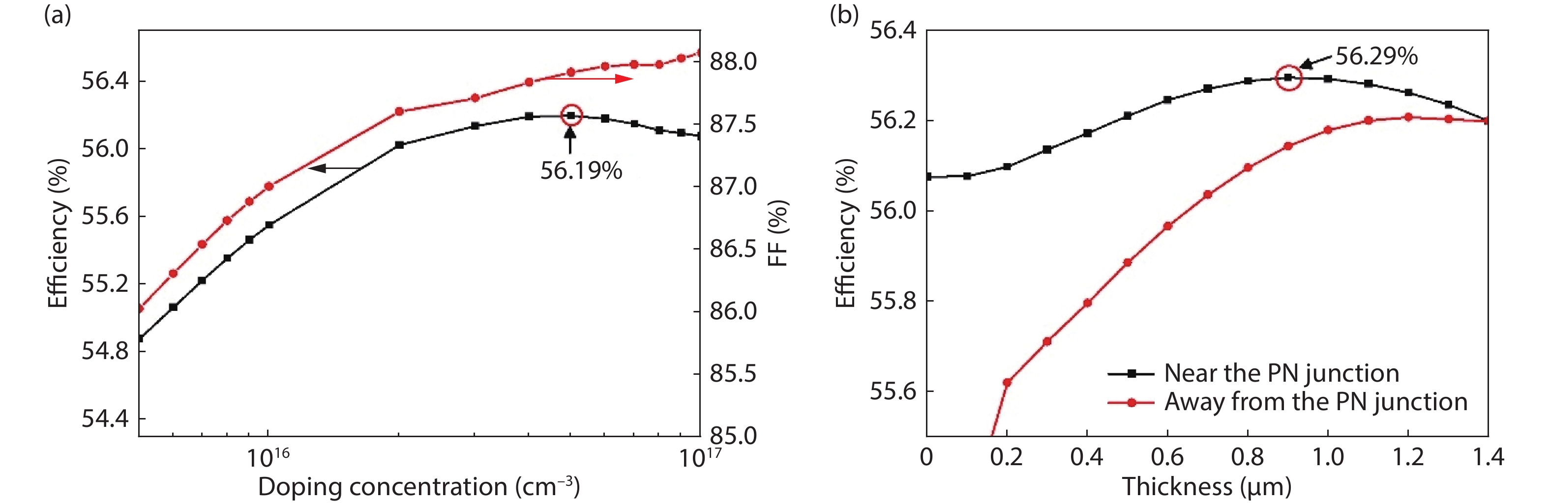
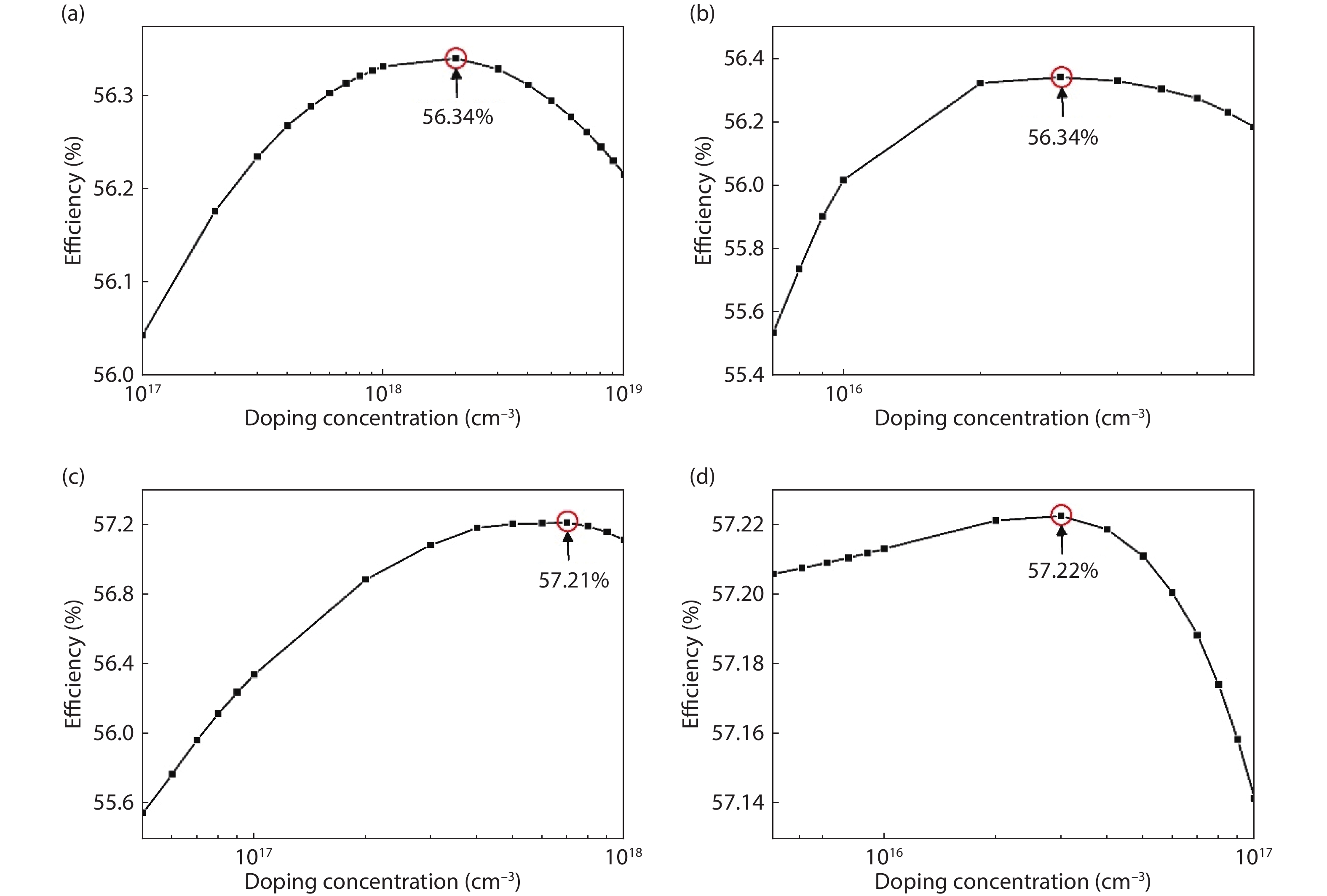
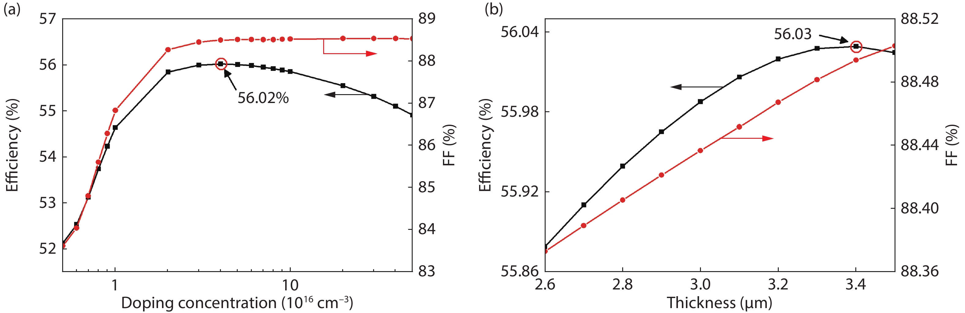
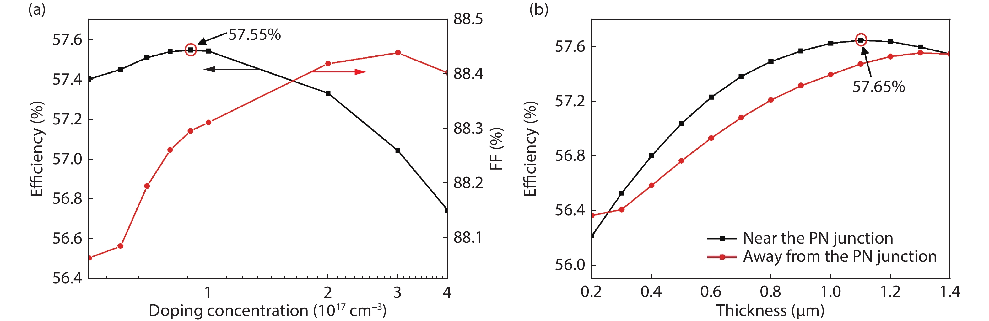
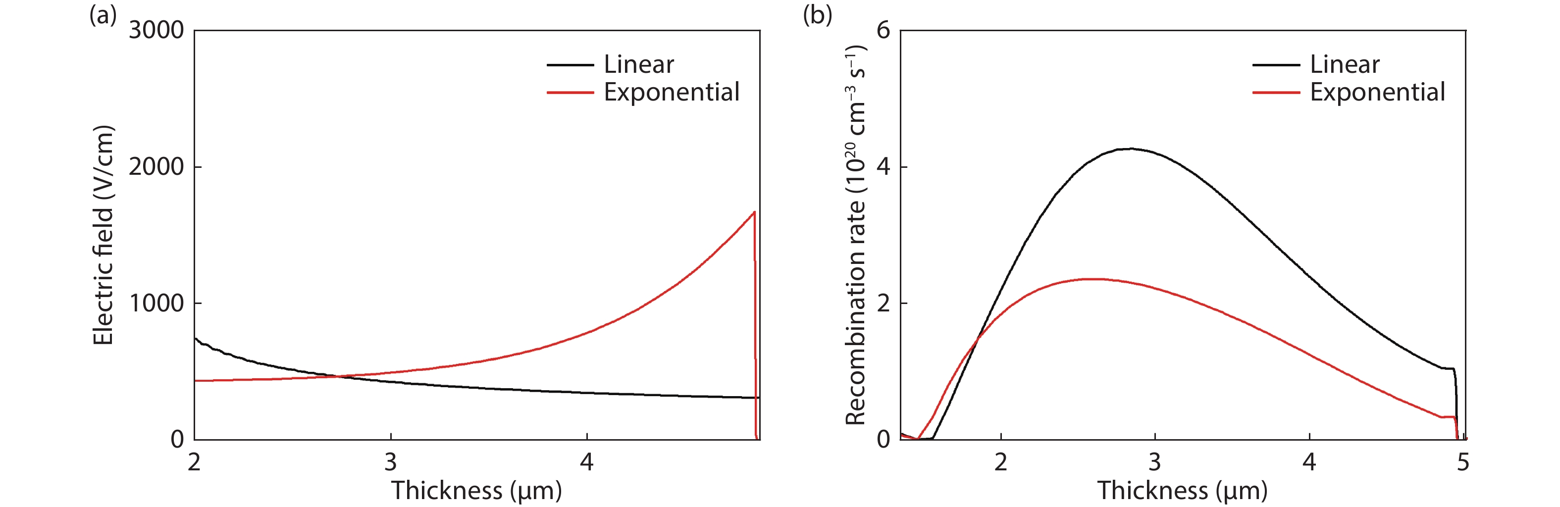
Abstract: The gradient doping regions were employed in the emitter layer and the base layer of GaAs based laser power converters (LPCs). Silvaco TCAD was used to numerically simulate the linear gradient doping and exponential gradient doping structure, and analyze the transport process of photogenerated carriers. Energy band adjustment via gradient doping improved the separation and transport efficiency of photogenerated carriers and reduced the total recombination rate of GaAs LPCs. Compared with traditional structure of LPCs, the photoelectric conversion efficiency of LPCs with linear and exponential gradient doping structure were improved from 52.7% to 57.2% and 57.7%, respectively, under 808 nm laser light at the power density of 1 W/cm2.

Key words: gradient dopinglaser power converters (LPCs)energy band adjustmentnumerical simulation

Following the introduction of the concept of a space-based solar power station, wireless energy transmission has once again entered our field of vision. Wireless energy transmission is mainly divided into microwave wireless energy transmission and laser wireless energy transmission. Due to the excellent directivity of lasers, low transmission loss, lack of electromagnetic interference during energy transmission, and compactness of the receiving device, laser wireless energy transmission has potential applications in various fields, such as precision instrument manufacturing and aerospace[1-6]. Laser power converters (LPCs) are one of the key components of laser wireless energy transmission systems.

To match the material band gap with the laser wavelength, numerous semiconductor materials have been used for different laser wavelength, such as GaAs for 808 nm laser light, InGaAs[7] and Si[8] for 1064 nm and GaInAsP[9] and GaSb[10] for 1550 nm. Among these materials, GaAs LPCs for converting the power of 808 nm laser light have attracted the most attention thanks to their well-characterized fabrication methods and high conversion efficiency [11-13].

In addition to the conventional structure[14, 15] of LPCs, numerous optimized structures have been recently reported, such as the no-cap-layer structure[16] adopted by Khvostikov et al., the selective rear-contact structure[17] proposed by Hwang et al. and the gradient doping structure[18] mentioned here. From a mathematical point of view, as shown in Fig. 1, there are four shapes of gradient doping structure[19]. But among them, logarithmic and smooth gradient doping have more than one variable, which is very complicated to simulate. Consequently, this article only selects linear and exponential gradient doping for discussion.

Figure  1.  The shapes of gradient doping structure. (a) Linear gradient doping. (b) Exponential gradient doping. (c) Logarithmic gradient doping. (d) Smooth gradient doping.

Owing to their epitaxial characteristics, the previously used LPCs all possess a uniform doping structure, therefore, the energy bands outside of the PN junction are approximately flat. Consequently, the photogenerated carriers generated in these regions are mainly transported via diffusion, which is very inefficient. Furthermore, those carries cannot be separated by diffusion along, resulting in severe recombination in this area. By introducing gradient doping regions into the conventional structure, the energy band can be adjusted purposefully, and forming a stable electric field in the gradient doping region[18, 20]. This electric field can assist the photogenerated electron–hole pairs generated in the gradient doping region in separation and transport, and reduce the recombination rate in these regions, and then improve the performance of LPCs[21].

To achieve the effect of improving the carrier transport, the energy band needs to be continuously tilted downward from the emitter layer to the base layer[20]. Therefore, the gradient doping region in the emitter layer and the base layer should be heavy-doped away from the junction region, and as the distance from the junction region gets closer, the doping concentration gradually decreases. The LPC structure used in this article is schematically illustrated in Fig. 2. The area surrounded by the red dotted line is a gradient doped region. The change in doping concentration is indicated by a gradient from green to blue, green indicates the heavy-doped region, and blue indicates the light-doped region. According to the difference of position of the gradient doping region in the emitter layer and the base layer, there are four different structures as shown in Fig. 2. And for linear and exponential gradient doping structure, there are a total of eight different structures (which are discussed in this article).

Figure  2.  (Color online) Structures of GaAs LPCs with different position of gradient doping region.

Silvaco TCAD was used to numerically simulate the structures mentioned above. From a mathematical point of view, there are thousands of specific doping methods for each structure. For calculation convenience and efficiency, we have simplified the discussion process. From the distribution of the recombination rate of the traditional structure (Fig. 3) we know that, the recombination of the base layer is mainly concentrated away from the junction region. When the gradient doping region in the base layer is near the junction region (Figs. 2(a) and 2(b)), the electric field generated by it cannot be effectively applied to the position with a higher recombination rate. Therefore, in theory, only when the gradient doping region is located away from the junction (Figs. 2(c) and 2(d)), can it effectively reduce the recombination rate, so we only need to discuss this structure later. But for emitter layer, the thickness of the emitter is relatively thin, the electric field generated by the window layer and the junction can extend to the inside of the emitter layer to a certain extent, so it is arduous to infer the optimal position of the gradient doping region in the emitter layer. As a result, both structures near and away from the junction region need to be discussed.

Figure  3.  Distribution of recombination rate in traditional structure of GaAs LPCs.

Therefore, the specific discussion method is: In the case where the entire base layer is doped gradually, the optimal doping concentration on the front (the incident surface of the laser) and back surfaces of the gradient doping region is determined first. Subsequently, the optimal thickness of gradient doping region in the base layer (the gradient doping region is away from the PN junction of LPC) is determined by simulation, until now the optimal doping parameters of the base region are maintained. Then, the emitter layer is discussed in the same way, and finally, the best gradient doping structure is determined. (To avoid band offset, the doping concentration of the non-gradually doping region on the front or back side of the gradient doping region is the same as that of the front or back surface of the gradient doping region, as shown in Fig. 1.) Based on the structure that we previously used, taking into account the actual situation and simplifying the discussion process, the doping concentration on the front surface (for convenience, we call it surface EF) of the gradient doping region in the emitter layer and the doping concentration on the back surface (for convenience, we call it surface BB) of the gradient doping region in the base layer are tentatively fixed at 1 × 10¹⁷ and 5 × 1018 cm–3, respectively[18].

The simulation results of the base layer of linear gradient doping LPC are shown in Fig. 4. When the entire base layer is doped gradually, as the doping concentration on the front surface gradually decreases (the difference between the doping concentration of front and back surface gradually increases), the photoelectric conversion efficiency of LPC first increases and then decreases (Fig. 4(a)). The highest efficiency is obtained when the doping concentration on the front surface is 3 × 1016 cm–3. This is because as the doping concentration on the front surface of the gradient doping region decreases, the internal electric field in the base layer increases (Fig. 5(a)), which facilitates the separation and transport of photogenerated electron–hole pairs generated here, The reduction recombination rate of the base layer (Fig. 5(b)), which in turn contributes to the improvement of VOC and FF of LPC. At the same time,

Figure  4.  (Color online) Simulation results of the base layer of linear gradient doping LPC. (a) Simulation about doping concentration when the gradient doping region thickness (GDT) in base layer is 1.5, 2.5, and 3.5 μm. (b) Simulation about the thickness of gradient doping region.
Figure  5.  (Color online) (a) Distribution of electric field in base layer with different front surface doping concentration. (b) Distribution of recombination rate in base layer with different front surface doping concentration.
VD=k0TqlnNDNAn2i,
(1)

where VD is the contact potential difference of the PN junction, k0 is the Boltzmann constant, T is the temperature, q is the electronic charge, ND and NA is the doping concentration of N and P region, ni is the intrinsic carrier concentration. It can be known from Eq. (1) that when the doping concentration on the front surface of the gradient doping region decreases, the electric field intensity and the potential difference VD of the junction region will decrease accordingly, which will lead to an increase in the recombination rate of the junction region and a decrease in the VOC of the device[21]. Therefore, when the doping concentration on the front surface of the gradient doping region is lower than a certain level, the influence of the junction region on the VOC and FF starts to play a leading role, which in turn leads to the reduction of the VOC and FF of LPC, and ultimately to the reduction of efficiency.

To confirm whether the optimal doping concentration on the front surface (For convenience, we call it surface BF) of gradient doping region in the base layer will change due to the change of the thickness of the gradient doping region, we also simulate it when the thickness of gradient doping region is 1.5 and 2.5 μm, respectively. The simulation result is shown in Fig. 4(a). It can be seen that the thickness of the gradient doping region does not affect the optimal doping concentration.

When the doping concentration on the front and back surfaces of the gradient doping region is unchanged, as the thickness of the gradient doping region decreases, the gradient of doping concentration in the gradient doping region gradually increases, and the internal electric field will gradually increase. And the photogenerated electron–hole pairs generated here will be more efficiently separated and transported. Therefore, the reduction of the thickness of the gradient doping region is beneficial to the reduction of the recombination rate inside the gradient doping region. But at the same time, the thickness of the non-gradient doping region will increase accordingly. Since there is no electric field in the non-gradient doping region, the recombination rate is relatively high. In other words, as the thickness of the gradient doping region gradually decreases, the overall recombination rate of the base layer will first decrease and then increase, which is obviously reflected in Fig. 4(b). With the gradual increase in the thickness of the gradient doping region of the base layer, the efficiency of LPC increases first and then decreases. The maximum efficiency is obtained when the thickness of the gradient doping region is 2.3 μm.

After the optimal structure of the base layer is obtained, the simulation results for the emitter layer are shown in Fig. 6. When the doping concentration on the back surface (for convenience, we call it surface EB) of the emitter layer is 5 × 1016 cm–3, and the thickness of the gradient doping region is 0.9 μm (the gradient doping region is close to the PN junction), the highest efficiency obtained is 56.29%.

Figure  6.  (Color online) Simulation results of the emitter layer of linear gradient doping LPC. (a) Simulation about doping concentration when the entire emitter layer is doped gradually. (b) Simulation about the thickness of gradient doping region in different position.

Since the doping concentration of surface EF and surface BB is tentatively fixed at 1 × 10¹⁷ and 5 × 1018 cm–3 before, in order to obtain the optimal doping concentration of them, after the optimal structure of linear gradient doping LPC is determined, we have carried out the simulation under the condition that the thickness and position of gradient doping region are unchanged. The specific simulation method is: The optimal doping concentration of surface BB is determined first, and then optimal doping concentration of surface BF is determined by simulation. As mentioned earlier, the optimal doping concentration of the gradient doping region is independent of the thickness, so there is no need to discuss the thickness of the gradient doping region at this time; then the optimal doping concentration of surface EF and surface EB will be obtained by the same method. The simulation results are shown in Fig. 7. When the doping concentration on the surface EF, EB, BF and BB are 7 × 10¹⁷, 3 × 10¹⁶, 3 × 10¹⁶ and 2 × 1018 cm–3, respectively, the highest efficiency obtained is 57.22%.

Figure  7.  Simulation about doping concentration on the (a) back and (b) front surface of the gradient doping region in base layer. Simulation about doping concentration on the (c) front and (d) back surface of the gradient doping region in emitter layer.

From the simulation results (Figs. 8 and 9) for exponential gradient doping structure (for the convenience of comparison, the doping concentration on surface EF and surface BB of exponential gradient doping structure are fixed at 7 × 10¹⁷ and 2 × 1018 cm–3, respectively) we know that, because this kind of gradient doping method and linear gradient doping are the same in the mechanism of improving the performance of LPC, the change trends of these two are similar. When the doping concentration on the surface BF is 6 ×1016 cm–3 and the thickness is 3.4 μm; when the doping concentration on the surface EB is 9 × 1016 cm–3 and the thickness is 1.1 μm, and the gradient doping region is near the junction, the highest efficiency obtained is 57.65%.

Figure  8.  (Color online) Simulation results of the base layer of exponential gradient doping LPC. (a) Simulation about doping concentration when the entire base layer is doped gradually. (b) Simulation about the thickness of gradient doping region
Figure  9.  (Color online) Simulation results of the emitter layer of exponential gradient doping LPC. (a) Simulation about doping concentration when the entire emitter layer is doped gradually. (b) Simulation about the thickness of gradient doping region in different position.

Due to the change rate of doping concentration of exponential gradient doping in the depth of the gradient doping region is significantly higher than the linear gradient (Fig. 1), in the depth of the gradient doping region, the exponential gradient can generate a larger electric field[20] (Fig. 10(a)), has the effect of better enhancing the separation and transport of photogenerated carriers and reducing the recombination rate (Fig. 10(b)). Therefore, after performing exponential gradient doping on both base and emitter layer, the device has achieved an efficiency of 57.65%, while linear gradient doping has only achieved a maximum efficiency of 57.22%. It can be seen that exponential gradient doping is more suitable for this kind LPC structure than linear gradient.

Figure  10.  (Color online) (a) Distribution of electric field in base layer of linear and exponential gradient doping LPCs. (b) Distribution of recombination rate in base layer of linear and exponential gradient doping LPCs.

Through the numerical simulation of LPC with different structures using two shapes of gradient doping methods, linear gradient, and exponential gradient, it is confirmed that the gradient doping method can effectively improve the separation and transport capacity and reduce the recombination rate of photogenerated carriers in the gradient doping region. Furthermore, the photoelectric conversion efficiency of LPC is improved. At the same time, compared to the linear gradient, the improvement of efficiency of the exponential gradient doping structure is more obvious. For exponential gradient doping structure, when the doping concentration of surface BF and surface BB are 6 × 10¹⁶ and 2 × 1018 cm–3, respectively, the thickness is 3.4 μm, and the gradient doping region is away from the junction region; the doping concentration of surface EF and surface EB are 7 × 10¹⁷ and 9 × 1016 cm–3, respectively, and the thickness is 1.1 μm, and the gradient doping region is close to the junction region, an efficiency of 57.65% is obtained.

This work was supported by the National Key R&D Program of China (No. 2018YFB1500500) and also supported by Ally Fund of Chinese Academy of Sciences (No. Y072051002).


[1]
Guan C, Liu W, Gao Q. Influence of the mesa electrode position on monolithic on-chip series-interconnect GaAs laser power converter performance. Mater Sci Semicond Process, 2018, 75, 136 doi: 10.1016/j.mssp.2017.11.027
[2]
Andreev V, Khvostikov V, Kalinovsky V, et al. High current density GaAs and GaSb photovoltaic cells for laser power beaming. Proceedings of 3rd World Conference on Photovoltaic Energy Conversion, 2003, 761
[3]
Fave A, Kaminski A, Gavand M, et al. GaAs converter for high power laser diode. Conference Record of the Twenty Fifth IEEE Photovoltaic Specialists Conference, 1996, 101
[4]
Guan C, Li L, Ji H M, et al. Fabrication and characterization of a high-power assembly with a 20-junction monolithically stacked laser power converter. IEEE J Photovolt, 2018, 8(5), 1355 doi: 10.1109/JPHOTOV.2018.2841195
[5]
Shi J W, Kuo F M, Yang C S, et al. Dynamic analysis of cascaded laser power converters for simultaneous high-speed data detection and optical-to-electrical DC power generation. IEEE Trans Electron Devices, 2011, 58(7), 2049 doi: 10.1109/TED.2011.2136379
[6]
Ding Y, Li Q, Lu Y, et al. TO-packaged, multi-junction GaAs laser power converter with output electric power over 1 W. Conference on Lasers and Electro-Optics Pacific Rim, 2017
[7]
Kalyuzhnyy N A, Emelyanov V M, Mintairov S A, et al. InGaAs metamorphic laser (λ = 1064 nm) power converters with over 44% efficiency. InAIP Conference Proceedings, 2018, 2012, 110002
[8]
Green M A, Zhao J, Wang A, et al. 45-percent efficient silicon photovoltaic cell under monochromatic light. IEEE Electron Device Lett, 1992, 13(6), 317 doi: 10.1109/55.145070
[9]
Jarvis S D, Sweeney S J, Perren M, et al. Development and characterisation of laser power converters for optical power transfer applications. IET Optoelectron, 2014, 8(2), 64 doi: 10.1049/iet-opt.2013.0066
[10]
Khvostikov V P, Sorokina S V, Khvostikova O A, et al. GaSb laser-power (λ = 1550 nm) converters: Fabrication method and characteristics. Semiconductors, 2016, 50(10), 1338 doi: 10.1134/S1063782616100146
[11]
Fafard S, York M C A, Proulx F, et al. Ultrahigh efficiencies in vertical epitaxial heterostructure architectures. Appl Phys Lett, 2016, 108(7), 071101 doi: 10.1063/1.4941240
[12]
Krut D, Sudharsanan R, Nishikawa W, et al. Monolithic multi-cell GaAs laser power converter with very high current density. Conference Record of the Twenty-Ninth IEEE Photovoltaic Specialists Conference, 2002, 908
[13]
Schubert J, Oliva E, Dimroth F, et al. High-voltage GaAs photovoltaic laser power converters. IEEE Trans Electron Devices, 2009, 56(2), 170 doi: 10.1109/TED.2008.2010603
[14]
Algora C, Diaz V. Performance and optimization of monochromatic p/n heteroface AlGaAs/GaAs photovoltaic cells. Solid-State Electron, 1997, 41(11), 1787 doi: 10.1016/S0038-1101(97)00147-0
[15]
Shan T Q, Qi X L. Design and optimization of GaAs photovoltaic converter for laser power beaming. Infrared Phys Technol, 2015, 71, 144 doi: 10.1016/j.infrared.2015.03.010
[16]
Khvostikov V P, Sorokina S V, Potapovich N S, et al. Modification of photovoltaic laser-power (λ = 808 nm) converters grown by LPE. Semiconductors, 2018, 52(3), 366 doi: 10.1134/S1063782618030120
[17]
Hwang S T, Hwang T, Lee S, et al. Selective rear contact for Ga0.5In0.5P- and GaAs-based solar cells. Sol Energy Mater Sol Cells, 2018, 182, 348 doi: 10.1016/j.solmat.2018.03.037
[18]
Zhao Y, Liang P, Ren H, et al. Enhanced efficiency in 808 nm GaAs laser power converters via gradient doping. AIP Adv, 2019, 9(10), 105206 doi: 10.1063/1.5109133
[19]
Hwang S T, Kim S, Cheun H, et al. Bandgap grading and Al0.3Ga0.7As heterojunction emitter for highly efficient GaAs-based solar cells. Sol Energy Mater Sol Cells, 2016, 155, 264 doi: 10.1016/j.solmat.2016.06.009
[20]
Liu E, Zhu B, Luo J. The physics of semiconductors. 7th ed. Beijing: Pubulishing House of Electronics Industry, 2011 (in Chinese)
[21]
Xioang S Z, Zhu M F. Foundation and application of solar cell. Beijing: Science Press, 2009 (in Chinese)
Fig. 1.  The shapes of gradient doping structure. (a) Linear gradient doping. (b) Exponential gradient doping. (c) Logarithmic gradient doping. (d) Smooth gradient doping.

Fig. 2.  (Color online) Structures of GaAs LPCs with different position of gradient doping region.

Fig. 3.  Distribution of recombination rate in traditional structure of GaAs LPCs.

Fig. 4.  (Color online) Simulation results of the base layer of linear gradient doping LPC. (a) Simulation about doping concentration when the gradient doping region thickness (GDT) in base layer is 1.5, 2.5, and 3.5 μm. (b) Simulation about the thickness of gradient doping region.

Fig. 5.  (Color online) (a) Distribution of electric field in base layer with different front surface doping concentration. (b) Distribution of recombination rate in base layer with different front surface doping concentration.

Fig. 6.  (Color online) Simulation results of the emitter layer of linear gradient doping LPC. (a) Simulation about doping concentration when the entire emitter layer is doped gradually. (b) Simulation about the thickness of gradient doping region in different position.

Fig. 7.  Simulation about doping concentration on the (a) back and (b) front surface of the gradient doping region in base layer. Simulation about doping concentration on the (c) front and (d) back surface of the gradient doping region in emitter layer.

Fig. 8.  (Color online) Simulation results of the base layer of exponential gradient doping LPC. (a) Simulation about doping concentration when the entire base layer is doped gradually. (b) Simulation about the thickness of gradient doping region

Fig. 9.  (Color online) Simulation results of the emitter layer of exponential gradient doping LPC. (a) Simulation about doping concentration when the entire emitter layer is doped gradually. (b) Simulation about the thickness of gradient doping region in different position.

Fig. 10.  (Color online) (a) Distribution of electric field in base layer of linear and exponential gradient doping LPCs. (b) Distribution of recombination rate in base layer of linear and exponential gradient doping LPCs.

[1]
Guan C, Liu W, Gao Q. Influence of the mesa electrode position on monolithic on-chip series-interconnect GaAs laser power converter performance. Mater Sci Semicond Process, 2018, 75, 136 doi: 10.1016/j.mssp.2017.11.027
[2]
Andreev V, Khvostikov V, Kalinovsky V, et al. High current density GaAs and GaSb photovoltaic cells for laser power beaming. Proceedings of 3rd World Conference on Photovoltaic Energy Conversion, 2003, 761
[3]
Fave A, Kaminski A, Gavand M, et al. GaAs converter for high power laser diode. Conference Record of the Twenty Fifth IEEE Photovoltaic Specialists Conference, 1996, 101
[4]
Guan C, Li L, Ji H M, et al. Fabrication and characterization of a high-power assembly with a 20-junction monolithically stacked laser power converter. IEEE J Photovolt, 2018, 8(5), 1355 doi: 10.1109/JPHOTOV.2018.2841195
[5]
Shi J W, Kuo F M, Yang C S, et al. Dynamic analysis of cascaded laser power converters for simultaneous high-speed data detection and optical-to-electrical DC power generation. IEEE Trans Electron Devices, 2011, 58(7), 2049 doi: 10.1109/TED.2011.2136379
[6]
Ding Y, Li Q, Lu Y, et al. TO-packaged, multi-junction GaAs laser power converter with output electric power over 1 W. Conference on Lasers and Electro-Optics Pacific Rim, 2017
[7]
Kalyuzhnyy N A, Emelyanov V M, Mintairov S A, et al. InGaAs metamorphic laser (λ = 1064 nm) power converters with over 44% efficiency. InAIP Conference Proceedings, 2018, 2012, 110002
[8]
Green M A, Zhao J, Wang A, et al. 45-percent efficient silicon photovoltaic cell under monochromatic light. IEEE Electron Device Lett, 1992, 13(6), 317 doi: 10.1109/55.145070
[9]
Jarvis S D, Sweeney S J, Perren M, et al. Development and characterisation of laser power converters for optical power transfer applications. IET Optoelectron, 2014, 8(2), 64 doi: 10.1049/iet-opt.2013.0066
[10]
Khvostikov V P, Sorokina S V, Khvostikova O A, et al. GaSb laser-power (λ = 1550 nm) converters: Fabrication method and characteristics. Semiconductors, 2016, 50(10), 1338 doi: 10.1134/S1063782616100146
[11]
Fafard S, York M C A, Proulx F, et al. Ultrahigh efficiencies in vertical epitaxial heterostructure architectures. Appl Phys Lett, 2016, 108(7), 071101 doi: 10.1063/1.4941240
[12]
Krut D, Sudharsanan R, Nishikawa W, et al. Monolithic multi-cell GaAs laser power converter with very high current density. Conference Record of the Twenty-Ninth IEEE Photovoltaic Specialists Conference, 2002, 908
[13]
Schubert J, Oliva E, Dimroth F, et al. High-voltage GaAs photovoltaic laser power converters. IEEE Trans Electron Devices, 2009, 56(2), 170 doi: 10.1109/TED.2008.2010603
[14]
Algora C, Diaz V. Performance and optimization of monochromatic p/n heteroface AlGaAs/GaAs photovoltaic cells. Solid-State Electron, 1997, 41(11), 1787 doi: 10.1016/S0038-1101(97)00147-0
[15]
Shan T Q, Qi X L. Design and optimization of GaAs photovoltaic converter for laser power beaming. Infrared Phys Technol, 2015, 71, 144 doi: 10.1016/j.infrared.2015.03.010
[16]
Khvostikov V P, Sorokina S V, Potapovich N S, et al. Modification of photovoltaic laser-power (λ = 808 nm) converters grown by LPE. Semiconductors, 2018, 52(3), 366 doi: 10.1134/S1063782618030120
[17]
Hwang S T, Hwang T, Lee S, et al. Selective rear contact for Ga0.5In0.5P- and GaAs-based solar cells. Sol Energy Mater Sol Cells, 2018, 182, 348 doi: 10.1016/j.solmat.2018.03.037
[18]
Zhao Y, Liang P, Ren H, et al. Enhanced efficiency in 808 nm GaAs laser power converters via gradient doping. AIP Adv, 2019, 9(10), 105206 doi: 10.1063/1.5109133
[19]
Hwang S T, Kim S, Cheun H, et al. Bandgap grading and Al0.3Ga0.7As heterojunction emitter for highly efficient GaAs-based solar cells. Sol Energy Mater Sol Cells, 2016, 155, 264 doi: 10.1016/j.solmat.2016.06.009
[20]
Liu E, Zhu B, Luo J. The physics of semiconductors. 7th ed. Beijing: Pubulishing House of Electronics Industry, 2011 (in Chinese)
[21]
Xioang S Z, Zhu M F. Foundation and application of solar cell. Beijing: Science Press, 2009 (in Chinese)
1

High performance terahertz laser

Quanyong Lu

Journal of Semiconductors, 2019, 40(2): 020203. doi: 10.1088/1674-4926/40/2/020203

2

Supersymmetric laser arrays

Chuanbo Li , Ming Li

Journal of Semiconductors, 2019, 40(4): 040201. doi: 10.1088/1674-4926/40/4/040201

3

Simulation and application of external quantum efficiency of solar cells based on spectroscopy

Guanlin Chen, Can Han, Lingling Yan, Yuelong Li, Ying Zhao, et al.

Journal of Semiconductors, 2019, 40(12): 122701. doi: 10.1088/1674-4926/40/12/122701

4

Characterizations of high-voltage vertically-stacked GaAs laser power converter

Jie Huang, Yurun Sun, Yongming Zhao, Shuzhen Yu, Kuilong Li, et al.

Journal of Semiconductors, 2018, 39(9): 094006. doi: 10.1088/1674-4926/39/9/094006

5

Four-junction AlGaAs/GaAs laser power converter

Jie Huang, Yurun Sun, Yongming Zhao, Shuzhen Yu, Jianrong Dong, et al.

Journal of Semiconductors, 2018, 39(4): 044003. doi: 10.1088/1674-4926/39/4/044003

6

Simulation study on single event burnout in linear doping buffer layer engineered power VDMOSFET

Jia Yunpeng, Su Hongyuan, Jin Rui, Hu Dongqing, Wu Yu, et al.

Journal of Semiconductors, 2016, 37(2): 024008. doi: 10.1088/1674-4926/37/2/024008

7

The calculation of band gap energy in zinc oxide films

Ali Arif, Okba Belahssen, Salim Gareh, Said Benramache

Journal of Semiconductors, 2015, 36(1): 013001. doi: 10.1088/1674-4926/36/1/013001

8

Numerical simulation of the effect of gold doping on the resistance to neutron irradiation of silicon diodes

K. Bekhouche, N. Sengouga, B. K. Jones

Journal of Semiconductors, 2015, 36(1): 014001. doi: 10.1088/1674-4926/36/1/014001

9

Analytical modeling and simulation of germanium single gate silicon on insulator TFET

T. S. Arun Samuel, N. B. Balamurugan

Journal of Semiconductors, 2014, 35(3): 034002. doi: 10.1088/1674-4926/35/3/034002

10

Low-power variable frequency PFC converters

Li Yani, Yang Yintang, Zhu Zhangming

Journal of Semiconductors, 2010, 31(1): 015008. doi: 10.1088/1674-4926/31/1/015008

11

Wall Temperature Simulation of a Radial Flow MOCVD Reactor with Three-Separate Vertical Inlets

Nie Yuhong, Liu Yong, Yao Shouguang

Chinese Journal of Semiconductors , 2007, 28(1): 127-130.

12

Numerical Explanation of Slow Transients in an AlGaN/GaN HEMT

Zhang Jinfeng, Hao Yue

Chinese Journal of Semiconductors , 2006, 27(2): 276-282.

13

Monte Carlo Simulation of Impurity Scattering Effect in Resonant-Phonon-Assisted Terahertz Quantum-Cascade Lasers

Cao Juncheng, Lü Jingtao

Chinese Journal of Semiconductors , 2006, 27(2): 304-308.

14

Lateral Oxidation in Vertical Cavity Surface Emitting Lasers

Liu Wenli, Hao Yongqin, Wang Yuxia, Jiang Xiaoguang, Feng Yuan, et al.

Chinese Journal of Semiconductors , 2006, 27(8): 1351-1354.

15

Decarbonization and Decolorization of Large Sapphire Crystals Grown by the Temperature Gradient Technique

Xu Jun, Zhou Guoqing, Deng Peizhen, Si Jiliang, Qian Xiaobo, et al.

Chinese Journal of Semiconductors , 2006, 27(2): 245-248.

16

Two-Dimensional Static Numerical Modeling and Simulation of AlGaN/GaN HEMT

Xue Lijun, Xia Yang, Liu Ming, Wang Yan, Shao Xue, et al.

Chinese Journal of Semiconductors , 2006, 27(2): 298-303.

17

Fabrication and Numerical Simulation of a Micromachined Contact Cantilever RF-MEMS Switch

Sun Jianhai, Cui Dafu, Xiao Jiang

Chinese Journal of Semiconductors , 2006, 27(2): 309-312.

18

Full Band Monte Carlo Simulation of Electron Transport in Ge with Anisotropic Scattering Process

Chen, Yong, and, Ravaioli, Umberto, et al.

Chinese Journal of Semiconductors , 2005, 26(3): 465-471.

19

1.55μm Laser Diode Monolithically Integrated with Spot-Size Converter Using Conventional Process

Hou Lianping, Wang Wei, and Zhu Hongliang

Chinese Journal of Semiconductors , 2005, 26(3): 443-447.

20

Simulation of a Monolithic Integrated CMOS Preamplifier for Neural Recordings

Sui Xiaohong, Liu Jinbin, Gu Ming, Pei Weihua, Chen Hongda, et al.

Chinese Journal of Semiconductors , 2005, 26(12): 2275-2280.

1. Fafard, S., Masson, D. 55% Efficient High-Power Multijunction Photovoltaic Laser Power Converters for 1070 nm. Photonics, 2025, 12(5): 406. doi:10.3390/photonics12050406
2. Saif, A.A., Mindil, A. Impact of using dual back surface field layers of different materials on GaAs single junction solar cell performance. Journal of Ovonic Research, 2024, 20(4): 569-577. doi:10.15251/JOR.2024.204.569
3. Fafard, S., Masson, D. Onset of Quantum-Confined Stark Effects in Multijunction Photovoltaic Laser Power Converters Designed with Thin Subcells. Photonics, 2023, 10(11): 1243. doi:10.3390/photonics10111243
4. Fafard, S., Masson, D. Vertical Multi-Junction Laser Power Converters with 61% Efficiency at 30 W Output Power and with Tolerance to Beam Non-Uniformity, Partial Illumination, and Beam Displacement. Photonics, 2023, 10(8): 940. doi:10.3390/photonics10080940
5. Zhang, Y., Guan, C., Chu, W. et al. Optimal I–V Curve Scan Time for a GaAs Laser Power Converter. Photonics, 2023, 10(7): 762. doi:10.3390/photonics10070762
6. Mekhtiyev, A., Dunayev, P., Neshina, Y. et al. POWER SUPPLY VIA FIBER-OPTICAL CONDUCTOR FOR SENSORS OF MINE WORKING MONITORING SYSTEM. Eastern European Journal of Enterprise Technologies, 2023, 5(5(125): 15-23. doi:10.15587/1729-4061.2023.289775
7. Fafard, S., Masson, D.P. 74.7% Efficient GaAs-Based Laser Power Converters at 808 nm at 150 K. Photonics, 2022, 9(8): 579. doi:10.3390/photonics9080579
8. Fafard, S., Masson, D.P. High‐Efficiency and High‐Power Multijunction InGaAs/InP Photovoltaic Laser Power Converters for 1470 nm. Photonics, 2022, 9(7): 438. doi:10.3390/photonics9070438
9. Fafard, S., Masson, D.P. Perspective on photovoltaic optical power converters. Journal of Applied Physics, 2021, 130(16): 160901. doi:10.1063/5.0070860
10. Fafard, S., Masson, D., Werthen, J.-G. et al. Power and spectral range characteristics for optical power converters. Energies, 2021, 14(15): 4395. doi:10.3390/en14154395
  • Search

    Advanced Search >>

    GET CITATION

    Yingjie Zhao, Shan Li, Huixue Ren, Shaojie Li, Peide Han. Energy band adjustment of 808 nm GaAs laser power converters via gradient doping[J]. Journal of Semiconductors, 2021, 42(3): 032701. doi: 10.1088/1674-4926/42/3/032701
    Y J Zhao, S Li, H X Ren, S J Li, P D Han, Energy band adjustment of 808 nm GaAs laser power converters via gradient doping[J]. J. Semicond., 2021, 42(3): 032701. doi: 10.1088/1674-4926/42/3/032701.
    shu

    Export: BibTex EndNote

    Article Metrics

    Article views: 3609 Times PDF downloads: 82 Times Cited by: 10 Times

    History

    Received: 13 January 2020 Revised: 23 June 2020 Online: Accepted Manuscript: 08 September 2020Uncorrected proof: 14 September 2020Published: 10 March 2021

    Catalog

      Email This Article

      User name:
      Email:*请输入正确邮箱
      Code:*验证码错误
      Yingjie Zhao, Shan Li, Huixue Ren, Shaojie Li, Peide Han. Energy band adjustment of 808 nm GaAs laser power converters via gradient doping[J]. Journal of Semiconductors, 2021, 42(3): 032701. doi: 10.1088/1674-4926/42/3/032701 ****Y J Zhao, S Li, H X Ren, S J Li, P D Han, Energy band adjustment of 808 nm GaAs laser power converters via gradient doping[J]. J. Semicond., 2021, 42(3): 032701. doi: 10.1088/1674-4926/42/3/032701.
      Citation:
      Yingjie Zhao, Shan Li, Huixue Ren, Shaojie Li, Peide Han. Energy band adjustment of 808 nm GaAs laser power converters via gradient doping[J]. Journal of Semiconductors, 2021, 42(3): 032701. doi: 10.1088/1674-4926/42/3/032701 ****
      Y J Zhao, S Li, H X Ren, S J Li, P D Han, Energy band adjustment of 808 nm GaAs laser power converters via gradient doping[J]. J. Semicond., 2021, 42(3): 032701. doi: 10.1088/1674-4926/42/3/032701.

      Energy band adjustment of 808 nm GaAs laser power converters via gradient doping

      DOI: 10.1088/1674-4926/42/3/032701
      More Information
      • Yingjie Zhao:In 2015, received a bachelor's degree in Applied Physics from University of Science and Technology Beijing. In 2020, received a Ph.D. from the Institute of Semiconductors, Chinese Academy of Sciences. During the Ph.D. study, working on high-efficiency laser power converters research with advisor Peide Han
      • Peide Han:with PhD degree, researcher (equivalent to professor) in the Institute of Semiconductors, Chinese Academy of Sciences. His main interested fields are photovoltaic, opto-electronic integration, semiconductor material and devices. With many national science foundations, he and his group have made much progress, including more than 100 papers publishing and 19 patents authorized
      • Corresponding author: pdhan@semi.ac.cn
      • Received Date: 2020-01-13
      • Revised Date: 2020-06-23
      • Published Date: 2021-03-10

      Catalog

        /

        DownLoad:  Full-Size Img  PowerPoint
        Return
        Return