Fig. 1.
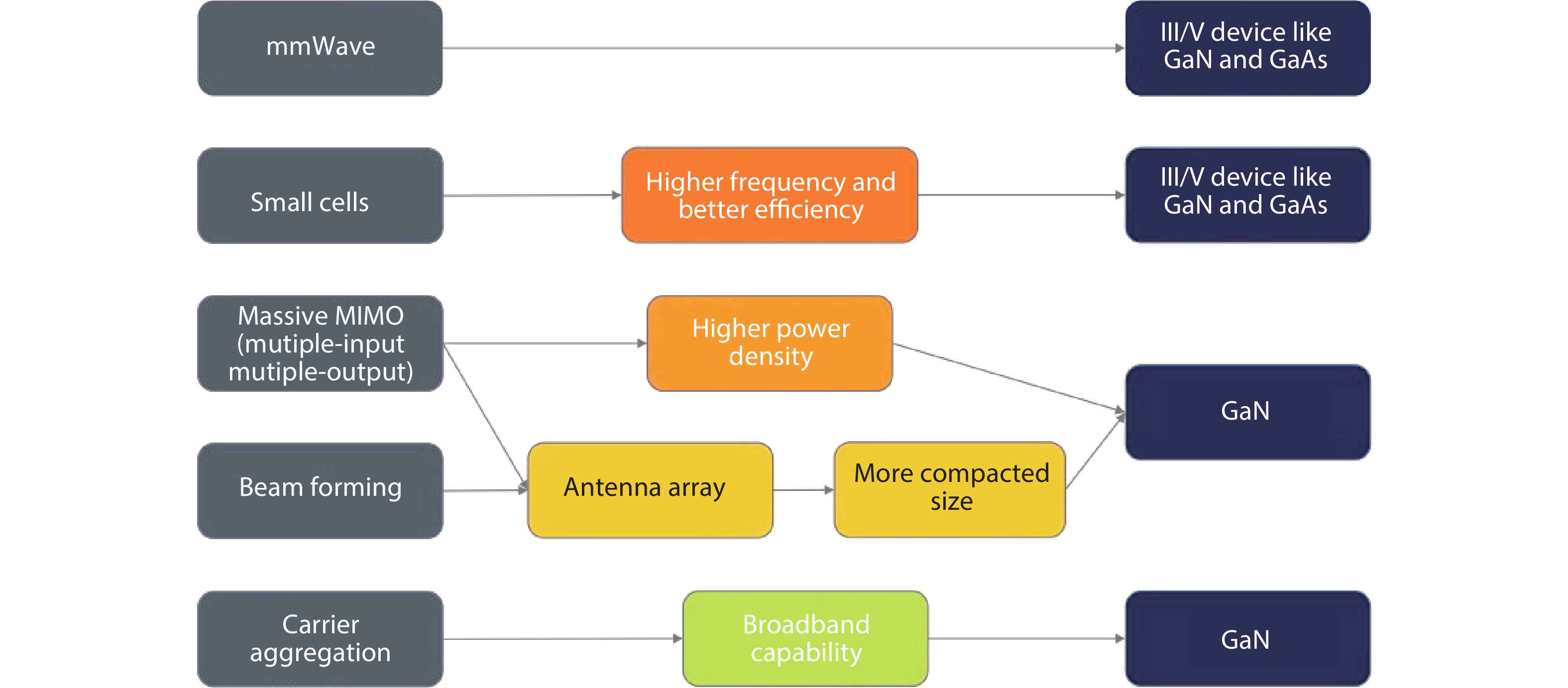
(Color online) The main requirements in 5G wireless communication[4].
REVIEWS
Xiaolong Cai1, 2, 3, Chenglin Du2, 3, Zixuan Sun2, 3, Ran Ye2, 3, Haijun Liu2, Yu Zhang2, Xiangyang Duan2 and Hai Lu1,
Corresponding author: Hai Lu, hailu@nju.edu.cn
Abstract: Gallium nitride (GaN)-based high-electron mobility transistors (HEMTs) are widely used in high power and high frequency application fields, due to the outstanding physical and chemical properties of the GaN material. However, GaN HEMTs suffer from degradations and even failures during practical applications, making physical analyses of post-failure devices extremely significant for reliability improvements and further device optimizations. In this paper, common physical characterization techniques for post failure analyses are introduced, several failure mechanisms and corresponding failure phenomena are reviewed and summarized, and finally device optimization methods are discussed.
Keywords: GaN, high electron mobility transistors, physical analysis, failure mechanism
| [1] |
Mi M H, Ma X H, Yang L, et al. Record combination fmax·Vbr of 25 THz·V in AlGaN/GaN HEMT with plasma treatment. AIP Adv, 2019, 9(4), 045212 doi: 10.1063/1.5090528
|
| [2] |
Panda D K, Amarnath G, Lenka T R, et al. Small-signal model parameter extraction of E-mode N-polar GaN MOS-HEMT using optimization algorithms and its comparison. J Semicond, 2018, 39(7), 64 doi: 10.1088/1674-4926/39/7/074001
|
| [3] |
Huang X, Fang R, Yang C, et al. Steep-slope field-effect transistors with AlGaN/GaN HEMT and oxide-based threshold switching device. Nanotechnology, 2019, 30(21), 215201 doi: 10.1088/1361-6528/ab0484
|
| [4] |
RF GaN market: applications, players, technology, and substrates 2018–2023 report. Yole Développement, 2018
|
| [5] |
Taylor A, Lu J, Zhu L, et al. Comparison of SiC MOSFET-based and GaN HEMT-based high-efficiency high-power-density 7.2 kW EV battery chargers. Power Electron, 2018, 11(11), 1849 doi: 10.1049/iet-pel.2017.0467
|
| [6] |
Faraji R, Farzanehfard H, Kampitsis G, et al. Fully soft-switched high step-up non-isolated three-port DC-DC converter using GaN HEMTs. IEEE Trans Ind Electron, 2020, 67(10), 8371 doi: 10.1109/TIE.2019.2944068
|
| [7] |
Chen X, Zhai W, Zhang J, et al. FEM thermal analysis of high power GaN-on-diamond HEMTs. J Semicond, 2018, 39(10), 104005 doi: 10.1088/1674-4926/39/10/104005
|
| [8] |
Power GaN 2018: epitaxy, devices, applications and technology trends. Yole Développement, 2018
|
| [9] |
Zanoni E. GaN HEMT reliability research – a white paper. University of Padova, Department of Information Engineering, 2017
|
| [10] |
Meneghini M, Rossetto I, Santi C D, et al. Reliability and failure analysis in power GaN-HEMTs: An overview. 2017 IEEE International Reliability Physics Symposium (IRPS), 2017, 3B-2.1
|
| [11] |
Rossetto I, Meneghini M, Tajalli A, et al. Evidence of hot-electron effects during hard switching of AlGaN/GaN HEMTs. IEEE Trans Electron Devices, 2017, 64(9), 3734 doi: 10.1109/TED.2017.2728785
|
| [12] |
Bajo M M, Sun H, Uren M J, et al. Time evolution of off-state degradation of AlGaN/GaN high electron mobility transistors. Appl Phys Lett, 2014, 104(22), 223506 doi: 10.1063/1.4881637
|
| [13] |
Luo T, Khursheed A. Elemental identification using transmitted and backscattered electrons in an SEM. Phys Procedia, 2008, 1(1), 155 doi: 10.1016/j.phpro.2008.07.091
|
| [14] |
Egerton R F. Physical principles of electron microscopy. Switzerland: Springer International Publishing, 2016
|
| [15] |
Gkanatsiou A, Lioutas C B, Frangis N, et al. Influence of 4H-SiC substrate miscut on the epitaxy and microstructure of AlGaN/GaN heterostructures. Mat Sci Semicond Proc, 2019, 91, 159 doi: 10.1016/j.mssp.2018.11.008
|
| [16] |
Wu Y, Chen C Y, Del Alamo J A. Electrical and structural degradation of GaN high electron mobility transistors under high-power and high-temperature direct current stress. J Appl Phys, 2015, 117(2), 025707 doi: 10.1063/1.4905677
|
| [17] |
Wang B, Islam Z, Haque A, et al. In situ transmission electron microscopy of transistor operation and failure. Nanotechnology, 2018, 29(31), 31LT01 doi: 10.1088/1361-6528/aac591
|
| [18] |
Marcon D, Meneghesso G, Wu T L, et al. Reliability analysis of permanent degradations on AlGaN/GaN HEMTs. IEEE Trans Electron Devices, 2013, 60(10), 3132 doi: 10.1109/TED.2013.2273216
|
| [19] |
Islam Z, Haque A, Glavin N. Real-time visualization of GaN/AlGaN high electron mobility transistor failure at off-state. Appl Phys Lett, 2018, 113(18), 183102 doi: 10.1063/1.5046178
|
| [20] |
Wang D D, Huang Y M, Tan P K, et al. Two planar polishing methods by using FIB technique: Toward ultimate top-down delayering for failure analysis. AIP Adv, 2015, 5(12), 127101 doi: 10.1063/1.4936941
|
| [21] |
Kumakura K, Makimoto T. Growth of GaN on sapphire substrates using novel buffer layers of ECR-plasma-sputtered Al2O3/graded-AlON/AlN/Al2O3. J Cryst Growth, 2006, 292(1), 155 doi: 10.1016/j.jcrysgro.2006.04.085
|
| [22] |
Rossetto I, Meneghini M, Barbato M, et al. Demonstration of field- and power-dependent ESD failure in AlGaN/GaN RF HEMTs. IEEE Trans Electron Devices, 2015, 62(9), 2830 doi: 10.1109/TED.2015.2463713
|
| [23] |
Shankar B, Shrivastava M. Unique ESD behavior and failure modes of AlGaN/GaN HEMTs. 2016 IEEE International Reliability Physics Symposium (IRPS), 2016, EL-7-1
|
| [24] |
Shankar B, Soni A, Singh M, et al. Trap assisted avalanche instability and safe operating area concerns in AlGaN/GaN HEMTs. 2017 IEEE International Reliability Physics Symposium (IRPS), 2017, WB-5.1
|
| [25] |
Shankar B, Soni A, Singh M, et al. ESD behavior of AlGaN/GaN HEMT on Si: Physical insights, design aspects, cumulative degradation and failure analysis. 2017 30th International Conference on VLSI Design and 2017 16th International Conference on Embedded Systems (VLSID), 2017, 361
|
| [26] |
Canato E, Meneghini M, Nardo A, et al. ESD-failure of E-mode GaN HEMTs: Role of device geometry and charge trapping. Microelectron Reliab, 2019, 100/101, 113334 doi: 10.1016/j.microrel.2019.06.026
|
| [27] |
Shankar B, Raghavan S, Shrivastava M. ESD reliability of AlGaN/GaN HEMT technology. IEEE Trans Electron Devices, 2019, 66(99), 3756 doi: 10.1109/TED.2019.2926781
|
| [28] |
Shankar B, Raghavan S, Shrivastava M. Distinct failure modes of AlGaN/GaN HEMTs under ESD conditions. IEEE Trans Electron Devices, 2020, 67(4), 1567 doi: 10.1109/TED.2020.2974508
|
| [29] |
Gao F, Tan S C, Del Alamo J A, et al. Impact of water-assisted electrochemical reactions on the off-state degradation of AlGaN/GaN HEMTs. IEEE Trans Electron Devices, 2014, 61(2), 437 doi: 10.1109/TED.2013.2293114
|
| [30] |
Rossetto I, Meneghini M, Pandey S, et al. Field-related failure of GaN-on-Si HEMTs: Dependence on device geometry and passivation. IEEE Trans Electron Devices, 2017, 64(1), 73 doi: 10.1109/TED.2016.2623774
|
| [31] |
Dammann M, Baeumler M, Polyakov V, et al. Reliability of 100 nm AlGaN/GaN HEMTs for mm-wave applications. Microelectron Reliab, 2017, 76/77, 292 doi: 10.1016/j.microrel.2017.07.008
|
| [32] |
Sin Y, Veksler D, Bonsall J, et al. Electrical and structural characteristics of aged RF GaN HEMTs and irradiated high-power GaN HEMTs with protons and heavy ions. Gallium Nitride Materials and Devices XIV, 2019, 10918
|
| [33] |
Whiting P G, Rudawski N G, Holzworth M R, et al. Nanocrack formation in AlGaN/GaN high electron mobility transistors utilizing Ti/Al/Ni/Au ohmic contacts. Microelectron Reliab, 2017, 70, 41 doi: 10.1016/j.microrel.2017.02.005
|
| [34] |
Mazumdar K, Kala S, Ghosal A, et al. Nanocrack formation due to inverse piezoelectric effect in AlGaN/GaN HEMT. Superlattice Microst, 2019, 125, 120 doi: 10.1016/j.spmi.2018.04.038
|
| [35] |
Zhu Q, Ma X, Hou B, et al. Investigation of inverse piezoelectric effect and trap effect in AlGaN/GaN HEMTs under reverse-bias step stress at cryogenic temperature. IEEE Access, 2020, 8, 35520 doi: 10.1109/ACCESS.2020.2975118
|
| [36] |
Liu S Y, Li S, Zhang C, et al. Single pulse unclamped-inductive-switching induced failure and analysis for 650 V p-GaN HEMT. IEEE Trans Power Electr, 2020, 35(11), 11328 doi: 10.1109/TPEL.2020.2988976
|
| [37] |
Temcamani F, Fonder J B, Latry O, et al. Electrical and physical analysis of thermal degradations of AlGaN/GaN HEMT under radar-type operating life. IEEE Trans Microw Theory, 2016, 64(3), 756 doi: 10.1109/TMTT.2016.2519342
|
| [38] |
Mocanu M, Unger C, Pfost M, et al. Thermal stability and failure mechanism of Schottky gate AlGaN/GaN HEMTs. IEEE Trans Electron Devices, 2017, 64(3), 848 doi: 10.1109/TED.2016.2633725
|
| [39] |
Unger C, Mocanu M, Ebli M, et al. A setup for very high temperature measurements of power semiconductors exceeding 500 °C. 2015 International Semiconductor Conference (CAS), 2015, 149
|
| [40] |
Jos R. Reverse Schottky gate current in AlGaN-GaN high-electron-mobility-transistors. J Appl Phys, 2012, 112(9), 94508 doi: 10.1063/1.4764866
|
| [41] |
Shin J H, Park J, Jang S Y, et al. Metal induced inhomogeneous Schottky barrier height in AlGaN/GaN Schottky diode. Appl Phys Lett, 2013, 102(24), 243505 doi: 10.1063/1.4811756
|
| [42] |
Nagahisa T, Ichijoh H, Suzuki T, et al. Robust 600 V GaN high electron mobility transistor technology on GaN-on-Si with 400 V, 5 μs load-short-circuit withstand capability. Jpn J Appl Phys, 2016, 55(4S), 04EG01 doi: 10.7567/JJAP.55.04EG01
|
| [43] |
Zhou L, San Z W, Hua Y J, et al. Investigation on failure mechanisms of GaN HEMT caused by high-power microwave (HPM) pulses. IEEE Trans Electromagn C, 2017, 59(3), 902 doi: 10.1109/TEMC.2016.2628046
|
| [44] |
Biener J, Hodge A M, Hamza A V, et al. Nanoporous Au: A high yield strength material. J Appl Phys, 2005, 97(2), 24301 doi: 10.1063/1.1832742
|
| [45] |
Alexopoulos P S. Mechanical properties of thin films. Annu Rev Mater Res, 1990, 20(1), 391 doi: 10.1146/annurev.ms.20.080190.002135
|
| [46] |
Sangwan V, Tan C M, Kapoor D, et al. Electromagnetic induced failure in GaN-HEMT high-frequency power amplifier. IEEE Trans Ind Electron, 2020, 67(7), 5708 doi: 10.1109/TIE.2019.2931233
|
| [47] |
Lei Z F, Guo H X, Tang M, et al. Degradation mechanisms of AlGaN/GaN HEMTs under 800 MeV Bi ions irradiation. Microelectron Reliab, 2018, 80, 312 doi: 10.1016/j.microrel.2017.07.086
|
| [48] |
Hu P, Liu J, Zhang S, et al. Degradation in AlGaN/GaN HEMTs irradiated with swift heavy ions: Role of latent tracks. Nucl Instrum Meth B, 2018, 430, 59 doi: 10.1016/j.nimb.2018.06.011
|
| [49] |
Islam Z, Paoletta A L, Monterrosa A M, et al. Heavy ion irradiation effects on GaN/AlGaN high electron mobility transistor failure at off-state. Microelectron Reliab, 2019, 102, 113493 doi: 10.1016/j.microrel.2019.113493
|
| [50] |
Nakamura K, Hanawa H, Horio K, et al. Analysis of breakdown voltages in AlGaN/GaN HEMTs with low-κ/high-κ double passivation layers. IEEE Trans Device Mat Res, 2019, 19(2), 298 doi: 10.1109/TDMR.2019.2903213
|
| [51] |
Shi Y T, Lu H, Xu W Z, et al. High-κ HfO2 based AlGaN/GaN MIS-HEMTs with Y2O3 interfacial layer for high gate controllability and interface quality. IEEE J Electron Devices, 2020, 8, 15 doi: 10.1109/JEDS.2019.2956844
|
| [52] |
Hanawa H, Onodera H, Nakajima A, et al. Numerical analysis of breakdown voltage enhancement in AlGaN/GaN HEMTs with a high-κ passivation layer. IEEE Trans Electron Devices, 2014, 61(3), 769 doi: 10.1109/TED.2014.2298194
|
| [53] |
Cheng L, Xu W, Pan D, et al. Gate-first process compatible, high-quality in situ SiNx for surface passivation and gate dielectrics in AlGaN/GaN MISHEMTs. J Phys D, 2019, 52(30), 305105 doi: 10.1088/1361-6463/ab1dc3
|
| [54] |
Shankar B, Soni A, Gupta S D, et al. On the trap assisted stress induced safe operating area limits of AlGaN/GaN HEMTs. 2018 IEEE International Reliability Physics Symposium (IRPS), 2018, 4E.4-1
|
| [55] |
Zeng C, Xu W, Xia Y, et al. Investigations of the gate instability characteristics in Schottky/ohmic type p-GaN gate normally-off AlGaN/GaN HEMTs. Appl Phys Express, 2019, 12(12), 121005 doi: 10.7567/1882-0786/ab52cc
|
| [56] |
Fletcher A S A, Nirmal D, Ajayan J, et al. Analysis of AlGaN/GaN HEMT using discrete field plate technique for high power and high frequency applications. AEU-Int J Electron C, 2019, 99, 325 doi: 10.1016/j.aeue.2018.12.006
|
| [57] |
Narang K, Bag R K, Singh V K, et al. Improvement in surface morphology and 2DEG properties of AlGaN/GaN HEMT. J Alloy Compd, 2020, 815, 152283 doi: 10.1016/j.jallcom.2019.152283
|
| [58] |
Wosko M, Szymanski T, Paszkiewicz B, et al. MOVPE growth conditions optimization for AlGaN/GaN/Si heterostructures with SiN and LT-AlN interlayers designed for HEMT applications. J Mater Sci-Mater El, 2019, 30(4), 4111 doi: 10.1007/s10854-019-00702-9
|
| [59] |
Jana D, Chatterjee A, Sharma T K. Confirmation of the compensation of unintentional donors in AlGaN/GaN HEMT structures by Mg-doping during initial growth of GaN buffer layer. J Lumin, 2019, 219, 116904 doi: 10.1016/j.jlumin.2019.116904
|
| [60] |
Borga M, Meneghini M, Benazzi D, et al. Buffer breakdown in GaN-on-Si HEMTs: A comprehensive study based on a sequential growth experiment. Microelectron Reliab, 2019, 100/101, 113461 doi: 10.1016/j.microrel.2019.113461
|
Table 1. Different failure mechanisms and their corresponding failure phenomena.
| Failure type | Failure mechanism | Failure phenomena | Ref. |
| ESD | Self-heating | Migration of S/D metal from D to S | [23, 27, 28] |
| Premature breakdown of parasitic SBD | Gate finger melts and migrates to S/D pads | ||
| Inverse piezoelectric effect | Crack in the G–D region | ||
| Trap assisted hole injection | Crack in the S–G region, which extend to buffer layer | [24, 27, 28] | |
| G–D electric field induced thermal stress | Crack propagate from G to D | ||
| Dislocation assisted current leakage | Gate finger peels off | [28] | |
| Electric stress induced defect generation | Crack and metal migration in the G–D region | [25] | |
| High electric stress | Electrochemical reaction with water | Pits, groove and trench along drain-side gate | [16, 29] |
| Passivation layer (SiNx) breakdown | Short-circuit path between gate edge and 2DEG | [30] | |
| Gate contact degradation | Metal migration at pads/AlGaN interface, crack | [31–33] | |
| Inverse piezoelectric effect | Burning around drain contact | [36] | |
| Dislocation assisted leakage current | Drain metal melt and penetrate to substrate | [19] | |
| High thermal stress | Gate contact degradation | Rimous metal surface, migration of Au into Ni-semiconductor Schottky contact | [37] |
| Self-heating | Burn marks in the G–D region | [38] | |
| Thermal expansion of FP metal | Crack in FP | [43] | |
| High magnetic field | Combined effect of the operating current density and the eddy current | Crack and small granule in the G–D region, liquid gate metal propagates into underlying layer | [46] |
| Irradiation effect | Irradiation damage | Latent track, vacancy and dislocation | [47–49] |
| Gate injection | Epitaxial layer peels off from substrate | [49] |
 DownLoad: CSV
| [1] |
Mi M H, Ma X H, Yang L, et al. Record combination fmax·Vbr of 25 THz·V in AlGaN/GaN HEMT with plasma treatment. AIP Adv, 2019, 9(4), 045212 doi: 10.1063/1.5090528
|
| [2] |
Panda D K, Amarnath G, Lenka T R, et al. Small-signal model parameter extraction of E-mode N-polar GaN MOS-HEMT using optimization algorithms and its comparison. J Semicond, 2018, 39(7), 64 doi: 10.1088/1674-4926/39/7/074001
|
| [3] |
Huang X, Fang R, Yang C, et al. Steep-slope field-effect transistors with AlGaN/GaN HEMT and oxide-based threshold switching device. Nanotechnology, 2019, 30(21), 215201 doi: 10.1088/1361-6528/ab0484
|
| [4] |
RF GaN market: applications, players, technology, and substrates 2018–2023 report. Yole Développement, 2018
|
| [5] |
Taylor A, Lu J, Zhu L, et al. Comparison of SiC MOSFET-based and GaN HEMT-based high-efficiency high-power-density 7.2 kW EV battery chargers. Power Electron, 2018, 11(11), 1849 doi: 10.1049/iet-pel.2017.0467
|
| [6] |
Faraji R, Farzanehfard H, Kampitsis G, et al. Fully soft-switched high step-up non-isolated three-port DC-DC converter using GaN HEMTs. IEEE Trans Ind Electron, 2020, 67(10), 8371 doi: 10.1109/TIE.2019.2944068
|
| [7] |
Chen X, Zhai W, Zhang J, et al. FEM thermal analysis of high power GaN-on-diamond HEMTs. J Semicond, 2018, 39(10), 104005 doi: 10.1088/1674-4926/39/10/104005
|
| [8] |
Power GaN 2018: epitaxy, devices, applications and technology trends. Yole Développement, 2018
|
| [9] |
Zanoni E. GaN HEMT reliability research – a white paper. University of Padova, Department of Information Engineering, 2017
|
| [10] |
Meneghini M, Rossetto I, Santi C D, et al. Reliability and failure analysis in power GaN-HEMTs: An overview. 2017 IEEE International Reliability Physics Symposium (IRPS), 2017, 3B-2.1
|
| [11] |
Rossetto I, Meneghini M, Tajalli A, et al. Evidence of hot-electron effects during hard switching of AlGaN/GaN HEMTs. IEEE Trans Electron Devices, 2017, 64(9), 3734 doi: 10.1109/TED.2017.2728785
|
| [12] |
Bajo M M, Sun H, Uren M J, et al. Time evolution of off-state degradation of AlGaN/GaN high electron mobility transistors. Appl Phys Lett, 2014, 104(22), 223506 doi: 10.1063/1.4881637
|
| [13] |
Luo T, Khursheed A. Elemental identification using transmitted and backscattered electrons in an SEM. Phys Procedia, 2008, 1(1), 155 doi: 10.1016/j.phpro.2008.07.091
|
| [14] |
Egerton R F. Physical principles of electron microscopy. Switzerland: Springer International Publishing, 2016
|
| [15] |
Gkanatsiou A, Lioutas C B, Frangis N, et al. Influence of 4H-SiC substrate miscut on the epitaxy and microstructure of AlGaN/GaN heterostructures. Mat Sci Semicond Proc, 2019, 91, 159 doi: 10.1016/j.mssp.2018.11.008
|
| [16] |
Wu Y, Chen C Y, Del Alamo J A. Electrical and structural degradation of GaN high electron mobility transistors under high-power and high-temperature direct current stress. J Appl Phys, 2015, 117(2), 025707 doi: 10.1063/1.4905677
|
| [17] |
Wang B, Islam Z, Haque A, et al. In situ transmission electron microscopy of transistor operation and failure. Nanotechnology, 2018, 29(31), 31LT01 doi: 10.1088/1361-6528/aac591
|
| [18] |
Marcon D, Meneghesso G, Wu T L, et al. Reliability analysis of permanent degradations on AlGaN/GaN HEMTs. IEEE Trans Electron Devices, 2013, 60(10), 3132 doi: 10.1109/TED.2013.2273216
|
| [19] |
Islam Z, Haque A, Glavin N. Real-time visualization of GaN/AlGaN high electron mobility transistor failure at off-state. Appl Phys Lett, 2018, 113(18), 183102 doi: 10.1063/1.5046178
|
| [20] |
Wang D D, Huang Y M, Tan P K, et al. Two planar polishing methods by using FIB technique: Toward ultimate top-down delayering for failure analysis. AIP Adv, 2015, 5(12), 127101 doi: 10.1063/1.4936941
|
| [21] |
Kumakura K, Makimoto T. Growth of GaN on sapphire substrates using novel buffer layers of ECR-plasma-sputtered Al2O3/graded-AlON/AlN/Al2O3. J Cryst Growth, 2006, 292(1), 155 doi: 10.1016/j.jcrysgro.2006.04.085
|
| [22] |
Rossetto I, Meneghini M, Barbato M, et al. Demonstration of field- and power-dependent ESD failure in AlGaN/GaN RF HEMTs. IEEE Trans Electron Devices, 2015, 62(9), 2830 doi: 10.1109/TED.2015.2463713
|
| [23] |
Shankar B, Shrivastava M. Unique ESD behavior and failure modes of AlGaN/GaN HEMTs. 2016 IEEE International Reliability Physics Symposium (IRPS), 2016, EL-7-1
|
| [24] |
Shankar B, Soni A, Singh M, et al. Trap assisted avalanche instability and safe operating area concerns in AlGaN/GaN HEMTs. 2017 IEEE International Reliability Physics Symposium (IRPS), 2017, WB-5.1
|
| [25] |
Shankar B, Soni A, Singh M, et al. ESD behavior of AlGaN/GaN HEMT on Si: Physical insights, design aspects, cumulative degradation and failure analysis. 2017 30th International Conference on VLSI Design and 2017 16th International Conference on Embedded Systems (VLSID), 2017, 361
|
| [26] |
Canato E, Meneghini M, Nardo A, et al. ESD-failure of E-mode GaN HEMTs: Role of device geometry and charge trapping. Microelectron Reliab, 2019, 100/101, 113334 doi: 10.1016/j.microrel.2019.06.026
|
| [27] |
Shankar B, Raghavan S, Shrivastava M. ESD reliability of AlGaN/GaN HEMT technology. IEEE Trans Electron Devices, 2019, 66(99), 3756 doi: 10.1109/TED.2019.2926781
|
| [28] |
Shankar B, Raghavan S, Shrivastava M. Distinct failure modes of AlGaN/GaN HEMTs under ESD conditions. IEEE Trans Electron Devices, 2020, 67(4), 1567 doi: 10.1109/TED.2020.2974508
|
| [29] |
Gao F, Tan S C, Del Alamo J A, et al. Impact of water-assisted electrochemical reactions on the off-state degradation of AlGaN/GaN HEMTs. IEEE Trans Electron Devices, 2014, 61(2), 437 doi: 10.1109/TED.2013.2293114
|
| [30] |
Rossetto I, Meneghini M, Pandey S, et al. Field-related failure of GaN-on-Si HEMTs: Dependence on device geometry and passivation. IEEE Trans Electron Devices, 2017, 64(1), 73 doi: 10.1109/TED.2016.2623774
|
| [31] |
Dammann M, Baeumler M, Polyakov V, et al. Reliability of 100 nm AlGaN/GaN HEMTs for mm-wave applications. Microelectron Reliab, 2017, 76/77, 292 doi: 10.1016/j.microrel.2017.07.008
|
| [32] |
Sin Y, Veksler D, Bonsall J, et al. Electrical and structural characteristics of aged RF GaN HEMTs and irradiated high-power GaN HEMTs with protons and heavy ions. Gallium Nitride Materials and Devices XIV, 2019, 10918
|
| [33] |
Whiting P G, Rudawski N G, Holzworth M R, et al. Nanocrack formation in AlGaN/GaN high electron mobility transistors utilizing Ti/Al/Ni/Au ohmic contacts. Microelectron Reliab, 2017, 70, 41 doi: 10.1016/j.microrel.2017.02.005
|
| [34] |
Mazumdar K, Kala S, Ghosal A, et al. Nanocrack formation due to inverse piezoelectric effect in AlGaN/GaN HEMT. Superlattice Microst, 2019, 125, 120 doi: 10.1016/j.spmi.2018.04.038
|
| [35] |
Zhu Q, Ma X, Hou B, et al. Investigation of inverse piezoelectric effect and trap effect in AlGaN/GaN HEMTs under reverse-bias step stress at cryogenic temperature. IEEE Access, 2020, 8, 35520 doi: 10.1109/ACCESS.2020.2975118
|
| [36] |
Liu S Y, Li S, Zhang C, et al. Single pulse unclamped-inductive-switching induced failure and analysis for 650 V p-GaN HEMT. IEEE Trans Power Electr, 2020, 35(11), 11328 doi: 10.1109/TPEL.2020.2988976
|
| [37] |
Temcamani F, Fonder J B, Latry O, et al. Electrical and physical analysis of thermal degradations of AlGaN/GaN HEMT under radar-type operating life. IEEE Trans Microw Theory, 2016, 64(3), 756 doi: 10.1109/TMTT.2016.2519342
|
| [38] |
Mocanu M, Unger C, Pfost M, et al. Thermal stability and failure mechanism of Schottky gate AlGaN/GaN HEMTs. IEEE Trans Electron Devices, 2017, 64(3), 848 doi: 10.1109/TED.2016.2633725
|
| [39] |
Unger C, Mocanu M, Ebli M, et al. A setup for very high temperature measurements of power semiconductors exceeding 500 °C. 2015 International Semiconductor Conference (CAS), 2015, 149
|
| [40] |
Jos R. Reverse Schottky gate current in AlGaN-GaN high-electron-mobility-transistors. J Appl Phys, 2012, 112(9), 94508 doi: 10.1063/1.4764866
|
| [41] |
Shin J H, Park J, Jang S Y, et al. Metal induced inhomogeneous Schottky barrier height in AlGaN/GaN Schottky diode. Appl Phys Lett, 2013, 102(24), 243505 doi: 10.1063/1.4811756
|
| [42] |
Nagahisa T, Ichijoh H, Suzuki T, et al. Robust 600 V GaN high electron mobility transistor technology on GaN-on-Si with 400 V, 5 μs load-short-circuit withstand capability. Jpn J Appl Phys, 2016, 55(4S), 04EG01 doi: 10.7567/JJAP.55.04EG01
|
| [43] |
Zhou L, San Z W, Hua Y J, et al. Investigation on failure mechanisms of GaN HEMT caused by high-power microwave (HPM) pulses. IEEE Trans Electromagn C, 2017, 59(3), 902 doi: 10.1109/TEMC.2016.2628046
|
| [44] |
Biener J, Hodge A M, Hamza A V, et al. Nanoporous Au: A high yield strength material. J Appl Phys, 2005, 97(2), 24301 doi: 10.1063/1.1832742
|
| [45] |
Alexopoulos P S. Mechanical properties of thin films. Annu Rev Mater Res, 1990, 20(1), 391 doi: 10.1146/annurev.ms.20.080190.002135
|
| [46] |
Sangwan V, Tan C M, Kapoor D, et al. Electromagnetic induced failure in GaN-HEMT high-frequency power amplifier. IEEE Trans Ind Electron, 2020, 67(7), 5708 doi: 10.1109/TIE.2019.2931233
|
| [47] |
Lei Z F, Guo H X, Tang M, et al. Degradation mechanisms of AlGaN/GaN HEMTs under 800 MeV Bi ions irradiation. Microelectron Reliab, 2018, 80, 312 doi: 10.1016/j.microrel.2017.07.086
|
| [48] |
Hu P, Liu J, Zhang S, et al. Degradation in AlGaN/GaN HEMTs irradiated with swift heavy ions: Role of latent tracks. Nucl Instrum Meth B, 2018, 430, 59 doi: 10.1016/j.nimb.2018.06.011
|
| [49] |
Islam Z, Paoletta A L, Monterrosa A M, et al. Heavy ion irradiation effects on GaN/AlGaN high electron mobility transistor failure at off-state. Microelectron Reliab, 2019, 102, 113493 doi: 10.1016/j.microrel.2019.113493
|
| [50] |
Nakamura K, Hanawa H, Horio K, et al. Analysis of breakdown voltages in AlGaN/GaN HEMTs with low-κ/high-κ double passivation layers. IEEE Trans Device Mat Res, 2019, 19(2), 298 doi: 10.1109/TDMR.2019.2903213
|
| [51] |
Shi Y T, Lu H, Xu W Z, et al. High-κ HfO2 based AlGaN/GaN MIS-HEMTs with Y2O3 interfacial layer for high gate controllability and interface quality. IEEE J Electron Devices, 2020, 8, 15 doi: 10.1109/JEDS.2019.2956844
|
| [52] |
Hanawa H, Onodera H, Nakajima A, et al. Numerical analysis of breakdown voltage enhancement in AlGaN/GaN HEMTs with a high-κ passivation layer. IEEE Trans Electron Devices, 2014, 61(3), 769 doi: 10.1109/TED.2014.2298194
|
| [53] |
Cheng L, Xu W, Pan D, et al. Gate-first process compatible, high-quality in situ SiNx for surface passivation and gate dielectrics in AlGaN/GaN MISHEMTs. J Phys D, 2019, 52(30), 305105 doi: 10.1088/1361-6463/ab1dc3
|
| [54] |
Shankar B, Soni A, Gupta S D, et al. On the trap assisted stress induced safe operating area limits of AlGaN/GaN HEMTs. 2018 IEEE International Reliability Physics Symposium (IRPS), 2018, 4E.4-1
|
| [55] |
Zeng C, Xu W, Xia Y, et al. Investigations of the gate instability characteristics in Schottky/ohmic type p-GaN gate normally-off AlGaN/GaN HEMTs. Appl Phys Express, 2019, 12(12), 121005 doi: 10.7567/1882-0786/ab52cc
|
| [56] |
Fletcher A S A, Nirmal D, Ajayan J, et al. Analysis of AlGaN/GaN HEMT using discrete field plate technique for high power and high frequency applications. AEU-Int J Electron C, 2019, 99, 325 doi: 10.1016/j.aeue.2018.12.006
|
| [57] |
Narang K, Bag R K, Singh V K, et al. Improvement in surface morphology and 2DEG properties of AlGaN/GaN HEMT. J Alloy Compd, 2020, 815, 152283 doi: 10.1016/j.jallcom.2019.152283
|
| [58] |
Wosko M, Szymanski T, Paszkiewicz B, et al. MOVPE growth conditions optimization for AlGaN/GaN/Si heterostructures with SiN and LT-AlN interlayers designed for HEMT applications. J Mater Sci-Mater El, 2019, 30(4), 4111 doi: 10.1007/s10854-019-00702-9
|
| [59] |
Jana D, Chatterjee A, Sharma T K. Confirmation of the compensation of unintentional donors in AlGaN/GaN HEMT structures by Mg-doping during initial growth of GaN buffer layer. J Lumin, 2019, 219, 116904 doi: 10.1016/j.jlumin.2019.116904
|
| [60] |
Borga M, Meneghini M, Benazzi D, et al. Buffer breakdown in GaN-on-Si HEMTs: A comprehensive study based on a sequential growth experiment. Microelectron Reliab, 2019, 100/101, 113461 doi: 10.1016/j.microrel.2019.113461
|


Article views: 9081 Times PDF downloads: 859 Times Cited by: 0 Times
Received: 24 July 2020 Revised: 10 November 2020 Online: Accepted Manuscript: 28 December 2020Uncorrected proof: 29 December 2020Published: 01 May 2021
| Citation: |
Xiaolong Cai, Chenglin Du, Zixuan Sun, Ran Ye, Haijun Liu, Yu Zhang, Xiangyang Duan, Hai Lu. Recent progress of physical failure analysis of GaN HEMTs[J]. Journal of Semiconductors, 2021, 42(5): 051801. doi: 10.1088/1674-4926/42/5/051801
****
X L Cai, C L Du, Z X Sun, R Ye, H J Liu, Y Zhang, X Y Duan, H Lu, Recent progress of physical failure analysis of GaN HEMTs[J]. J. Semicond., 2021, 42(5): 051801. doi: 10.1088/1674-4926/42/5/051801.

|
| [1] |
Mi M H, Ma X H, Yang L, et al. Record combination fmax·Vbr of 25 THz·V in AlGaN/GaN HEMT with plasma treatment. AIP Adv, 2019, 9(4), 045212 doi: 10.1063/1.5090528
|
| [2] |
Panda D K, Amarnath G, Lenka T R, et al. Small-signal model parameter extraction of E-mode N-polar GaN MOS-HEMT using optimization algorithms and its comparison. J Semicond, 2018, 39(7), 64 doi: 10.1088/1674-4926/39/7/074001
|
| [3] |
Huang X, Fang R, Yang C, et al. Steep-slope field-effect transistors with AlGaN/GaN HEMT and oxide-based threshold switching device. Nanotechnology, 2019, 30(21), 215201 doi: 10.1088/1361-6528/ab0484
|
| [4] |
RF GaN market: applications, players, technology, and substrates 2018–2023 report. Yole Développement, 2018
|
| [5] |
Taylor A, Lu J, Zhu L, et al. Comparison of SiC MOSFET-based and GaN HEMT-based high-efficiency high-power-density 7.2 kW EV battery chargers. Power Electron, 2018, 11(11), 1849 doi: 10.1049/iet-pel.2017.0467
|
| [6] |
Faraji R, Farzanehfard H, Kampitsis G, et al. Fully soft-switched high step-up non-isolated three-port DC-DC converter using GaN HEMTs. IEEE Trans Ind Electron, 2020, 67(10), 8371 doi: 10.1109/TIE.2019.2944068
|
| [7] |
Chen X, Zhai W, Zhang J, et al. FEM thermal analysis of high power GaN-on-diamond HEMTs. J Semicond, 2018, 39(10), 104005 doi: 10.1088/1674-4926/39/10/104005
|
| [8] |
Power GaN 2018: epitaxy, devices, applications and technology trends. Yole Développement, 2018
|
| [9] |
Zanoni E. GaN HEMT reliability research – a white paper. University of Padova, Department of Information Engineering, 2017
|
| [10] |
Meneghini M, Rossetto I, Santi C D, et al. Reliability and failure analysis in power GaN-HEMTs: An overview. 2017 IEEE International Reliability Physics Symposium (IRPS), 2017, 3B-2.1
|
| [11] |
Rossetto I, Meneghini M, Tajalli A, et al. Evidence of hot-electron effects during hard switching of AlGaN/GaN HEMTs. IEEE Trans Electron Devices, 2017, 64(9), 3734 doi: 10.1109/TED.2017.2728785
|
| [12] |
Bajo M M, Sun H, Uren M J, et al. Time evolution of off-state degradation of AlGaN/GaN high electron mobility transistors. Appl Phys Lett, 2014, 104(22), 223506 doi: 10.1063/1.4881637
|
| [13] |
Luo T, Khursheed A. Elemental identification using transmitted and backscattered electrons in an SEM. Phys Procedia, 2008, 1(1), 155 doi: 10.1016/j.phpro.2008.07.091
|
| [14] |
Egerton R F. Physical principles of electron microscopy. Switzerland: Springer International Publishing, 2016
|
| [15] |
Gkanatsiou A, Lioutas C B, Frangis N, et al. Influence of 4H-SiC substrate miscut on the epitaxy and microstructure of AlGaN/GaN heterostructures. Mat Sci Semicond Proc, 2019, 91, 159 doi: 10.1016/j.mssp.2018.11.008
|
| [16] |
Wu Y, Chen C Y, Del Alamo J A. Electrical and structural degradation of GaN high electron mobility transistors under high-power and high-temperature direct current stress. J Appl Phys, 2015, 117(2), 025707 doi: 10.1063/1.4905677
|
| [17] |
Wang B, Islam Z, Haque A, et al. In situ transmission electron microscopy of transistor operation and failure. Nanotechnology, 2018, 29(31), 31LT01 doi: 10.1088/1361-6528/aac591
|
| [18] |
Marcon D, Meneghesso G, Wu T L, et al. Reliability analysis of permanent degradations on AlGaN/GaN HEMTs. IEEE Trans Electron Devices, 2013, 60(10), 3132 doi: 10.1109/TED.2013.2273216
|
| [19] |
Islam Z, Haque A, Glavin N. Real-time visualization of GaN/AlGaN high electron mobility transistor failure at off-state. Appl Phys Lett, 2018, 113(18), 183102 doi: 10.1063/1.5046178
|
| [20] |
Wang D D, Huang Y M, Tan P K, et al. Two planar polishing methods by using FIB technique: Toward ultimate top-down delayering for failure analysis. AIP Adv, 2015, 5(12), 127101 doi: 10.1063/1.4936941
|
| [21] |
Kumakura K, Makimoto T. Growth of GaN on sapphire substrates using novel buffer layers of ECR-plasma-sputtered Al2O3/graded-AlON/AlN/Al2O3. J Cryst Growth, 2006, 292(1), 155 doi: 10.1016/j.jcrysgro.2006.04.085
|
| [22] |
Rossetto I, Meneghini M, Barbato M, et al. Demonstration of field- and power-dependent ESD failure in AlGaN/GaN RF HEMTs. IEEE Trans Electron Devices, 2015, 62(9), 2830 doi: 10.1109/TED.2015.2463713
|
| [23] |
Shankar B, Shrivastava M. Unique ESD behavior and failure modes of AlGaN/GaN HEMTs. 2016 IEEE International Reliability Physics Symposium (IRPS), 2016, EL-7-1
|
| [24] |
Shankar B, Soni A, Singh M, et al. Trap assisted avalanche instability and safe operating area concerns in AlGaN/GaN HEMTs. 2017 IEEE International Reliability Physics Symposium (IRPS), 2017, WB-5.1
|
| [25] |
Shankar B, Soni A, Singh M, et al. ESD behavior of AlGaN/GaN HEMT on Si: Physical insights, design aspects, cumulative degradation and failure analysis. 2017 30th International Conference on VLSI Design and 2017 16th International Conference on Embedded Systems (VLSID), 2017, 361
|
| [26] |
Canato E, Meneghini M, Nardo A, et al. ESD-failure of E-mode GaN HEMTs: Role of device geometry and charge trapping. Microelectron Reliab, 2019, 100/101, 113334 doi: 10.1016/j.microrel.2019.06.026
|
| [27] |
Shankar B, Raghavan S, Shrivastava M. ESD reliability of AlGaN/GaN HEMT technology. IEEE Trans Electron Devices, 2019, 66(99), 3756 doi: 10.1109/TED.2019.2926781
|
| [28] |
Shankar B, Raghavan S, Shrivastava M. Distinct failure modes of AlGaN/GaN HEMTs under ESD conditions. IEEE Trans Electron Devices, 2020, 67(4), 1567 doi: 10.1109/TED.2020.2974508
|
| [29] |
Gao F, Tan S C, Del Alamo J A, et al. Impact of water-assisted electrochemical reactions on the off-state degradation of AlGaN/GaN HEMTs. IEEE Trans Electron Devices, 2014, 61(2), 437 doi: 10.1109/TED.2013.2293114
|
| [30] |
Rossetto I, Meneghini M, Pandey S, et al. Field-related failure of GaN-on-Si HEMTs: Dependence on device geometry and passivation. IEEE Trans Electron Devices, 2017, 64(1), 73 doi: 10.1109/TED.2016.2623774
|
| [31] |
Dammann M, Baeumler M, Polyakov V, et al. Reliability of 100 nm AlGaN/GaN HEMTs for mm-wave applications. Microelectron Reliab, 2017, 76/77, 292 doi: 10.1016/j.microrel.2017.07.008
|
| [32] |
Sin Y, Veksler D, Bonsall J, et al. Electrical and structural characteristics of aged RF GaN HEMTs and irradiated high-power GaN HEMTs with protons and heavy ions. Gallium Nitride Materials and Devices XIV, 2019, 10918
|
| [33] |
Whiting P G, Rudawski N G, Holzworth M R, et al. Nanocrack formation in AlGaN/GaN high electron mobility transistors utilizing Ti/Al/Ni/Au ohmic contacts. Microelectron Reliab, 2017, 70, 41 doi: 10.1016/j.microrel.2017.02.005
|
| [34] |
Mazumdar K, Kala S, Ghosal A, et al. Nanocrack formation due to inverse piezoelectric effect in AlGaN/GaN HEMT. Superlattice Microst, 2019, 125, 120 doi: 10.1016/j.spmi.2018.04.038
|
| [35] |
Zhu Q, Ma X, Hou B, et al. Investigation of inverse piezoelectric effect and trap effect in AlGaN/GaN HEMTs under reverse-bias step stress at cryogenic temperature. IEEE Access, 2020, 8, 35520 doi: 10.1109/ACCESS.2020.2975118
|
| [36] |
Liu S Y, Li S, Zhang C, et al. Single pulse unclamped-inductive-switching induced failure and analysis for 650 V p-GaN HEMT. IEEE Trans Power Electr, 2020, 35(11), 11328 doi: 10.1109/TPEL.2020.2988976
|
| [37] |
Temcamani F, Fonder J B, Latry O, et al. Electrical and physical analysis of thermal degradations of AlGaN/GaN HEMT under radar-type operating life. IEEE Trans Microw Theory, 2016, 64(3), 756 doi: 10.1109/TMTT.2016.2519342
|
| [38] |
Mocanu M, Unger C, Pfost M, et al. Thermal stability and failure mechanism of Schottky gate AlGaN/GaN HEMTs. IEEE Trans Electron Devices, 2017, 64(3), 848 doi: 10.1109/TED.2016.2633725
|
| [39] |
Unger C, Mocanu M, Ebli M, et al. A setup for very high temperature measurements of power semiconductors exceeding 500 °C. 2015 International Semiconductor Conference (CAS), 2015, 149
|
| [40] |
Jos R. Reverse Schottky gate current in AlGaN-GaN high-electron-mobility-transistors. J Appl Phys, 2012, 112(9), 94508 doi: 10.1063/1.4764866
|
| [41] |
Shin J H, Park J, Jang S Y, et al. Metal induced inhomogeneous Schottky barrier height in AlGaN/GaN Schottky diode. Appl Phys Lett, 2013, 102(24), 243505 doi: 10.1063/1.4811756
|
| [42] |
Nagahisa T, Ichijoh H, Suzuki T, et al. Robust 600 V GaN high electron mobility transistor technology on GaN-on-Si with 400 V, 5 μs load-short-circuit withstand capability. Jpn J Appl Phys, 2016, 55(4S), 04EG01 doi: 10.7567/JJAP.55.04EG01
|
| [43] |
Zhou L, San Z W, Hua Y J, et al. Investigation on failure mechanisms of GaN HEMT caused by high-power microwave (HPM) pulses. IEEE Trans Electromagn C, 2017, 59(3), 902 doi: 10.1109/TEMC.2016.2628046
|
| [44] |
Biener J, Hodge A M, Hamza A V, et al. Nanoporous Au: A high yield strength material. J Appl Phys, 2005, 97(2), 24301 doi: 10.1063/1.1832742
|
| [45] |
Alexopoulos P S. Mechanical properties of thin films. Annu Rev Mater Res, 1990, 20(1), 391 doi: 10.1146/annurev.ms.20.080190.002135
|
| [46] |
Sangwan V, Tan C M, Kapoor D, et al. Electromagnetic induced failure in GaN-HEMT high-frequency power amplifier. IEEE Trans Ind Electron, 2020, 67(7), 5708 doi: 10.1109/TIE.2019.2931233
|
| [47] |
Lei Z F, Guo H X, Tang M, et al. Degradation mechanisms of AlGaN/GaN HEMTs under 800 MeV Bi ions irradiation. Microelectron Reliab, 2018, 80, 312 doi: 10.1016/j.microrel.2017.07.086
|
| [48] |
Hu P, Liu J, Zhang S, et al. Degradation in AlGaN/GaN HEMTs irradiated with swift heavy ions: Role of latent tracks. Nucl Instrum Meth B, 2018, 430, 59 doi: 10.1016/j.nimb.2018.06.011
|
| [49] |
Islam Z, Paoletta A L, Monterrosa A M, et al. Heavy ion irradiation effects on GaN/AlGaN high electron mobility transistor failure at off-state. Microelectron Reliab, 2019, 102, 113493 doi: 10.1016/j.microrel.2019.113493
|
| [50] |
Nakamura K, Hanawa H, Horio K, et al. Analysis of breakdown voltages in AlGaN/GaN HEMTs with low-κ/high-κ double passivation layers. IEEE Trans Device Mat Res, 2019, 19(2), 298 doi: 10.1109/TDMR.2019.2903213
|
| [51] |
Shi Y T, Lu H, Xu W Z, et al. High-κ HfO2 based AlGaN/GaN MIS-HEMTs with Y2O3 interfacial layer for high gate controllability and interface quality. IEEE J Electron Devices, 2020, 8, 15 doi: 10.1109/JEDS.2019.2956844
|
| [52] |
Hanawa H, Onodera H, Nakajima A, et al. Numerical analysis of breakdown voltage enhancement in AlGaN/GaN HEMTs with a high-κ passivation layer. IEEE Trans Electron Devices, 2014, 61(3), 769 doi: 10.1109/TED.2014.2298194
|
| [53] |
Cheng L, Xu W, Pan D, et al. Gate-first process compatible, high-quality in situ SiNx for surface passivation and gate dielectrics in AlGaN/GaN MISHEMTs. J Phys D, 2019, 52(30), 305105 doi: 10.1088/1361-6463/ab1dc3
|
| [54] |
Shankar B, Soni A, Gupta S D, et al. On the trap assisted stress induced safe operating area limits of AlGaN/GaN HEMTs. 2018 IEEE International Reliability Physics Symposium (IRPS), 2018, 4E.4-1
|
| [55] |
Zeng C, Xu W, Xia Y, et al. Investigations of the gate instability characteristics in Schottky/ohmic type p-GaN gate normally-off AlGaN/GaN HEMTs. Appl Phys Express, 2019, 12(12), 121005 doi: 10.7567/1882-0786/ab52cc
|
| [56] |
Fletcher A S A, Nirmal D, Ajayan J, et al. Analysis of AlGaN/GaN HEMT using discrete field plate technique for high power and high frequency applications. AEU-Int J Electron C, 2019, 99, 325 doi: 10.1016/j.aeue.2018.12.006
|
| [57] |
Narang K, Bag R K, Singh V K, et al. Improvement in surface morphology and 2DEG properties of AlGaN/GaN HEMT. J Alloy Compd, 2020, 815, 152283 doi: 10.1016/j.jallcom.2019.152283
|
| [58] |
Wosko M, Szymanski T, Paszkiewicz B, et al. MOVPE growth conditions optimization for AlGaN/GaN/Si heterostructures with SiN and LT-AlN interlayers designed for HEMT applications. J Mater Sci-Mater El, 2019, 30(4), 4111 doi: 10.1007/s10854-019-00702-9
|
| [59] |
Jana D, Chatterjee A, Sharma T K. Confirmation of the compensation of unintentional donors in AlGaN/GaN HEMT structures by Mg-doping during initial growth of GaN buffer layer. J Lumin, 2019, 219, 116904 doi: 10.1016/j.jlumin.2019.116904
|
| [60] |
Borga M, Meneghini M, Benazzi D, et al. Buffer breakdown in GaN-on-Si HEMTs: A comprehensive study based on a sequential growth experiment. Microelectron Reliab, 2019, 100/101, 113461 doi: 10.1016/j.microrel.2019.113461
|

 WeChat ID
Journal of Semiconductors © 2017 All Rights Reserved 京ICP备05085259号-2