Processing math: 100%
J. Semicond. > 2021, Volume 42 > Issue 7 > 072701

ARTICLES

Structural and electrical characterization of Cu2ZnSnS4 ingot material grown by melting method

S. Kerour1, 2, A. Bouloufa1, 2, , M. Lasladj1, 2, K. Djessas3 and K. Medjnoun3

+ Author Affiliations

 Corresponding author: A. Bouloufa, abdeslam_bouloufa@yahoo.fr

DOI: 10.1088/1674-4926/42/7/072701

PDF

Turn off MathJax

Abstract: In this work, a Cu2ZnSnS4 (CZTS) ingot is grown via a melting method, then cooled; the resulting molten stoichiometric mixture is sealed off in a quartz ampoule under vacuum. The CZTS powder chemical composition analyses are determined using energy dispersive spectroscopy, and revealing the slightly Cu-rich and Zn-poor character of the ingot. Powder X-ray diffraction analysis reveals a crystalline structure with a kesterite phase formation, and a preferred orientation of (112) plane. The lattice constants of the a- and c- axes, calculated based on the XRD analyses, are a = 5.40 Å and c = 10.84 Å. Based on Hall measurements at room temperature, we find that the crystal exhibits p-type conductivity, with a high concentration of 1018 cm–3, a resistivity of 1.7 Ω cm, and a mobility of 10.69 cm2V–1s–1. Activation energies are estimated based on an Arrhenius plot of conductivity versus 1/T, for a temperature range of 80–350 K, measuring 35 and 160 meV in low- and high-temperature regimes, respectively, which is attributed to complex defects (2CuZn+SnZn) and antisite defects (CuZn), respectively. The observed scattering mechanisms are attributed to ionized impurities and acoustic phonons at low and high temperatures, respectively. The extracted band-gap is 1.37 eV.

Key words: Cu2ZnSnS4growthmelting methodkesteriteHall measurements

Solar energy is probably one of the promising renewable resources, and is currently attracting a great deal of attention[1]. In recent years, CuInxGa1–xSe2 (CIGS) thin-film solar cells have achieved a record conversion efficiency of 22.9%[2] up to as much as 23.35%[3]. Unfortunately, the scarcity of Indium, and the high cost of both indium and gallium resources could severely impede CIGS solar cell efficiency in the near future[4]. It is therefore necessary to establish a novel, earth-abundant, and low-cost absorber material for next-generation solar cells. Recently, Cu2ZnSnS4 (CZTS), Cu2ZnSnSe4 (CZTSe), and Cu2ZnSn(S,Se)4 (CZTSSe) quaternary compounds have been recognized as among the most attractive materials for large-scale future deployment[5-8]. CZTS is a p-type semiconductor kesterite crystalline structure, with a high absorption coefficient of 104 cm–1 in the visible range of the spectrum, and a direct bandgap, Eg, of about 1.45 eV[9-11]. Owing to the similarity of its physical properties to those of CIGS, as well as the relative abundance of its constituent elements, CZTS has become one of the most promising absorber layer materials for future photovoltaic applications[12-14]. Most recently, solar cells based on the alloy CZTSSe have achieved 12.6% power conversion efficiency[15]. However, this is still lower than the Shockley–Queisser limit of 32%[16].

Despite the fact that the growth and characterization of CZTS single crystals have been the focus of several studies, achieving a better understanding of the fundamental properties of this material, in an attempt to achieve higher efficiency, remains challenging. In fact, CZTS single crystals have been prepared by various methods, such as the directional freezing method[17], solid state reaction[18, 19], the traveling heater method[20, 21] and the Bridgman technique[22]. Such processing techniques require costly and heavy equipment; as such, the melting growth technique may be advantageous for the growth of single crystals.

In this work, a low cost and simple technique based on thermal melt, which is widely used in the growth of high-quality single crystal of several photovoltaic absorbers[23-25], is used to grow a polycrystalline CZTS ingot. Growth parameters such as ampoule dimensions, process thermal profile, and the partial vapor pressure of the constituent elements are studied in depth in order for growth to succeed, and to achieve the best compound crystallization. The potential of the melt growth technique is assessed, along with the growth results, and the characterization of a CZTS single crystal. Compositional and structural properties are investigated in order to identify the obtained compound. The electrical properties are analyzed at low and high temperatures to gain further evidence as to the fundamental properties of the as-grown ingot.

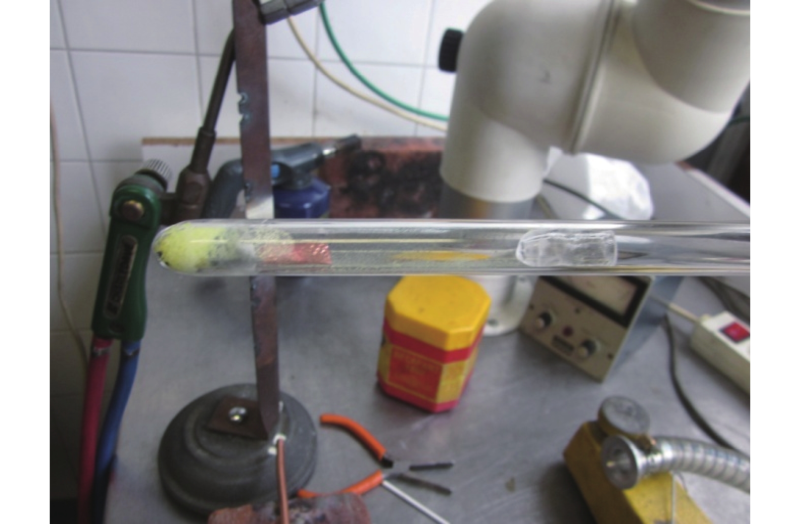
The CZTS single crystal was grown by cooling a molten stoichiometric of copper Cu (6N), zinc Zn (4N), tin Sn (5N) and sulfur S (5N) elements. The Cu : Zn : Sn : S constituents were weighed in 2 : 1 : 1 : 4 atomic proportions, placed into a quartz ampoule with dimensions of 200 mm length, and 14 mm diameter, and sealed off using an oxygen-acetylene blowpipe, under a pressure of 6.66 × 10⁻⁵ Pa. The vacuum inside the ampoule was verified via high-voltage ionizing excitation. Fig. 1 shows the ampoule containing the constituent elements. The ampoule was then inserted into a horizontal tubular CARBOLITE furnace, connected to a temperature regulator. The mixture was heated from room temperature to 400 °C at a rate of 0.5 °C/min, and maintained at this temperature for 24 h, followed by an increase to 700 °C. This step was followed to suppress the potential explosive reaction occurring between S and the other elements. The ampoule was then heated to 1100 °C at a rate of 0.33 °C/min, and held at this temperature for 24 h to ensure the mixing and homogeneity of the melt. Heating to this high temperature reduces void formation in the ingot. Microcracking and bulk cracking are usually encountered if cooling rates are too high[26]. As such, the ampoule was slowly cooled to 900 °C, at a cooling rate of 0.166 °C/min, and maintained at this temperature for 12 h, followed by further cooling to 700 °C at the same rate in order to ensure successful crystal growth. For the temperature range from 700–300 °C, the cooling rate was increased to 0.5 °C/min. Finally, the furnace was switched off, allowing the ampoule to reach room temperature. The CZTS ingot removed from the ampoule measured about 25 mm. Using an agate mortar, the solid ingot was reduced into powder, so as to facilitate analysis of its various characterizations.

Figure  1.  The ampoule containing the constituent elements of CZTS under evacuation.

The chemical composition of the powdered CZTS was analyzed by means of energy-dispersive spectroscopy (EDS) using a Jeol-JSM-6400 scanning electron microscope, operating at a 20 kV acceleration voltage. The crystal structure and lattice constants were examined via powder X-ray diffraction (XRD), where the pattern was collected using an Empyrean PANalytical powder diffractometer, with Cu Kα radiation (λ = 1.54056 Å), and Bragg-Brentano θ–2θ focusing geometry. The XRD scan was conducted in the range of 2θ = 20°–80°, with a step width of 0.02°. Electrical transport properties were investigated using an Ecopia HMS 5300 Hall measurement system under a 0.56 T magnetic field in the Van der Pauw geometry. The temperature-dependence of the Hall Effect measurement was carried out over a temperature range of 80–350 K. Samples cut from the ingot, measuring 5 × 4 × 1.6 mm3 were polished with 2400 to 4000 grain/cm2 sandpaper with Al2O3 powder, using a MICATECH Z34 polishing machine. Cu contacts of 0.8 mm of diameter were deposited onto the sample via Physical Vapor Deposition (PVD), to a thickness of 200 nm. These contacts were adequate for Van der Pauw measurements, although they were strictly Ohmic for p-type CZTS.

Growth of CZTS from the melt is complicated by major obstacles, such as the exothermic reactions of sulfur with other elements, and the increase in pressure during heating. This can lead to explosive fracture and loss of ampoules, and, in the worst-case scenario, loss of the furnace tube; it is therefore necessary to understand the reaction mechanisms. The partial vapor pressure of sulfur is of great importance in relation to the melting growth of CZTS bulk crystals. According to Ref. [27], it is given by the relation:

logP=4830T5logT+21.049(Bar,K).
(1)

The pressure at 1100 °C reaches 6.3 × 10⁶ Pa. This high pressure can lead to the explosion of the ampoule[28, 29]. To avoid damage to the ampoule, it is therefore necessary to decrease the pressure inside it via the formation of binary and ternary sulfides, which have lower partial vapor pressure than sulfur[30]. Binary sulfides start to form from 213 °C for SnS[31], 419 °C for ZnS[32], and 435 °C for CuS[33]. The CZTS phase formation occurs based on one of two reaction pathways[34]:

CuS/Cu2S+ZnS+SnS/SnS2 (±S)Cu2ZnSnS4,CuS/Cu2S+ZnS+SnS/SnS2 (±S)Cu2SnS3+ZnSCu2ZnSnS4.

Fig. 2 shows the obtained 2.5 cm length ingot.

Figure  2.  The obtained ingot of CZTS.

EDS measurements were performed at multiple points along the ingot. Chemical composition as an atomic percentage is summarized in Table 1.

Table  1.  Chemical composition of CZTS.
Atomic composition (%)Cu/(Zn+Sn)Zn/Sn
CuZnSnS
Point 131.6111.6812.8843.831.280.9
Point 227.7310.2412.0749.961.240.85
Average29.6710.9612.4746.891.260.88
DownLoad: CSV  | Show Table

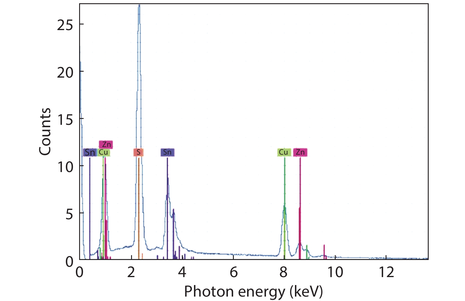
The average indicates the near stoichiometry of the ingot, with a slight deficiency in sulfur, due primarily to its volatility and high vapor pressure. The small quantity of remaining powder when introducing elements into the ampoule may be the cause of the slight deficiency in zinc. The EDS measurements show a Cu/(Zn+Sn) ratio of 1.26, and a Zn/Sn ratio of 0.88. Even this deviation from the stoichiometric ratios results mainly from a high population of intrinsic defects. Ref. [35] reported in their study that the cluster (2CuZn+SnZn) defect, which has a low formation energy (0.2–0.6 eV), should be the highest population defect, contributing to the high Cu/(Zn+Sn) and low Zn/Sn ratios. A typical EDS spectrum is acquired to investigate the homogeneity of elemental composition. The spectrum in Fig. 3 shows a uniform distribution of the ingot’s constituent elements.

Figure  3.  EDS spectrum of CZTS ingot.

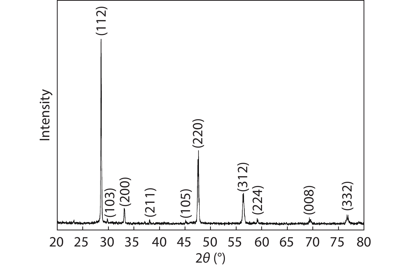
The powder XRD pattern of the as-grown ingot is shown in Fig. 4. The strong diffraction peak around 2θ = 28.62° corresponds to the (112) crystal plane of the kesterite CZTS structure. Multiple reflection peaks, centered at 2θ = 33.1°, 47.62°, 56.4°, and 76.58° correspond, respectively, to the (200), (220), (312) and (332) planes of kesterite CZTS (JCPDS card no. 026-0575).

Figure  4.  Powder XRD pattern of the as-grown ingot.

As CZTS has a tetragonal structure, the lattice constants of the a- and c- axes were calculated using Eq. (2):

1d2=h2+k2a2+l2c2,
(2)

where d is the spacing between the planes, and (hkl) are the Miller indices. Lattice constants were found to be a = 5.40 Å, and c = 10.84 Å. Both of these results agree well with the reported values of a = 5.435 Å and c = 10.85 Å in Ref. [36], and a = 5.429 Å and c = 10.847 Å in Ref. [22]. Full width at half maximum (FWHM) was estimated using the mean derived from the Fytick software package[37] for the main characteristic peak (112) located at 28.62°, and measured 0.16°. This narrow FWHM indicates the high-quality single-crystalline nature of the synthesized ingot. No secondary phases, such as SnxSy, or Cu2–xS, were identified in the XRD pattern.

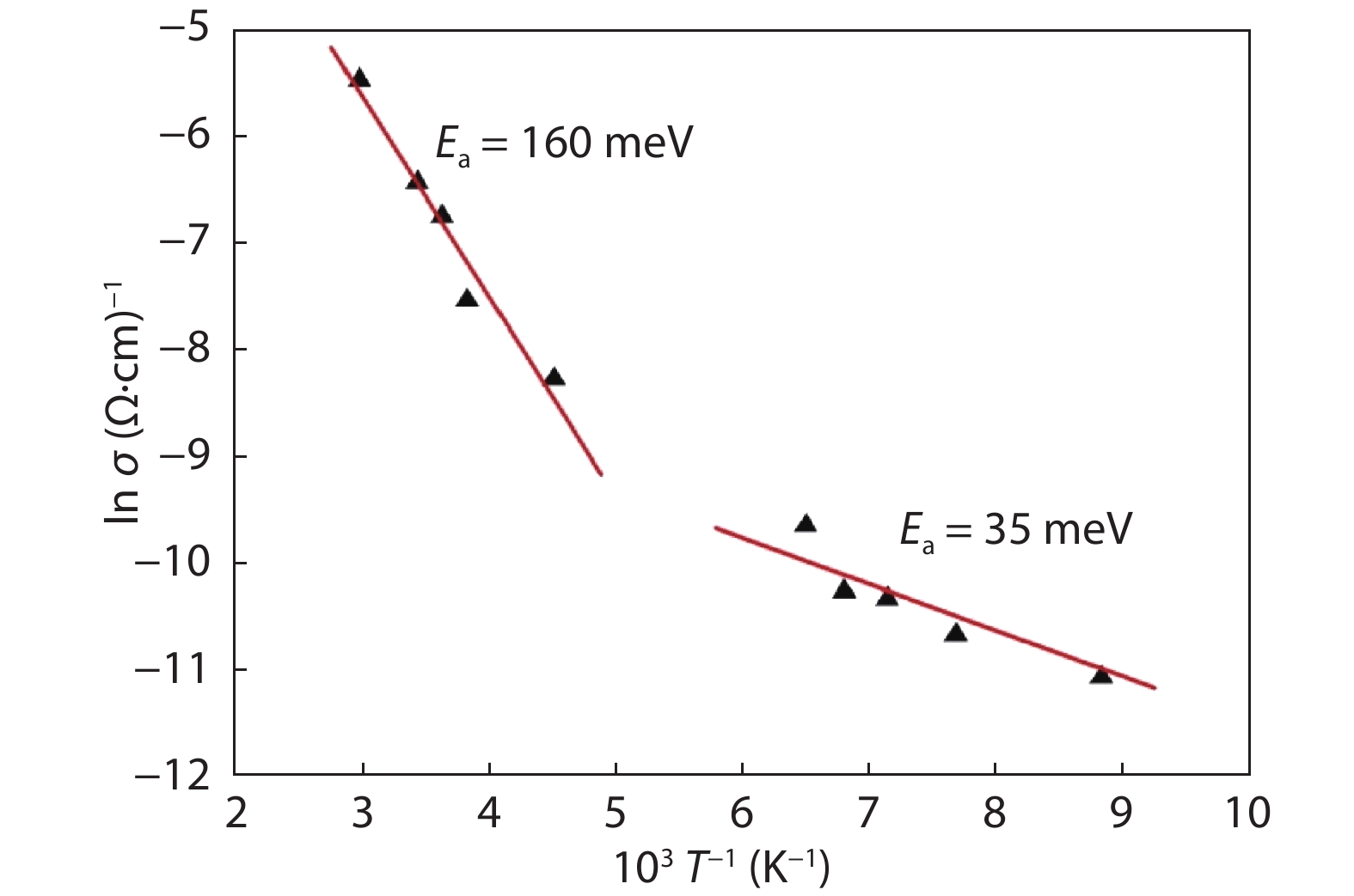
The electrical properties of the samples were determined via Hall measurements at room temperature. The ingot was found to exhibit p-type conductivity. A high p-concentration of 1.29 × 1018 cm–3, and a low resistivity, ρ, of 1.7 Ω cm were measured. This higher concentration has been widely reported in samples with the ratio Cu/(Zn+Sn) > 1, and is ascribed to the fact that the ionization of the intrinsic acceptor defects produces holes; a high population of defects results in high carrier concentration. Several previous results have indicated that resistivity decreases with an increasing Cu/(II+IV) atomic ratio in some Cu2–II–IV–VI4 semiconductors, such as CZTS and CZTSe[3840]. The hole mobility, µp, was then measured, and found to be 10.69 cm2V–1s–1. This value is in good agreement with that reported in the literature[41, 42]. In order to investigate the properties of CZTS bulk crystal in more detail, the temperature dependence of Hall measurement was calculated for a temperature range of 80– 350 K. Activation energies of 35 and 160 meV, for low- and high-temperature regimes, respectively, were extracted from the Arrhenius plot of ln σ versus 1/T (Fig. 5) using the Petritz model[43]:

Figure  5.  Arrhenius plot of ln σ versus reverse temperature.
σ=σ0exp(EaKBT),
(3)

where σ is the conductivity, σ0 is the pre-exponential term, KB is the Boltzmann constant, T is the absolute temperature, and Ea is the activation energy related to the defects in the CZTS. An activation energy of 35 meV may be associated with the transition energy of shallow defects in the (2CuZn+SnZn) cluster; however, the activation energy in the high-temperature regime of 160 meV agrees well with the calculated (–/0) level of CuZn antisite acceptor defects (ionized from neutral to (–1) charge), as reported by Ref. [35]. In that study, the authors demonstrated that the presence of both (2CuZn+SnZn) and CuZn antisite defects in Cu-rich compounds corresponds to high carrier concentration (~ 1018 cm–3). This value of concentration agrees well with the 1.29 × 1018 cm–3 measurement obtained for a CZTS single crystal in this work.

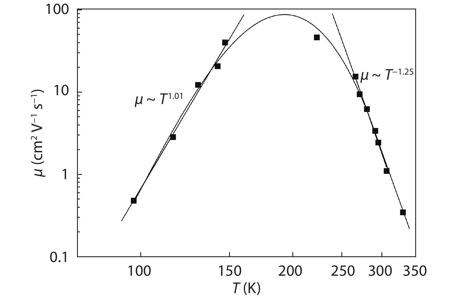
The charge carriers may be scattered by various mechanisms; as such the transport properties depend strongly on the type of scattering mechanism involved. Fig. 6 depicts the temperature- dependence of the mobility, in order to determine these mechanisms. In the low-temperature range below 150 K, the sample shows a power-law behavior, with an exponent of 1.01; this value would indicate that the dominant scattering mechanism is ionized impurity scattering. At higher temperatures (above 200 K), the mobility shows a steeper decrease, with a power-law exponent of –1.25, indicating that the mobility is dominated by acoustic phonon scattering[44, 45].

Figure  6.  Temperature dependence of mobility.

As the semiconductor’s aspect at high temperatures seems intrinsic, the hole concentration is defined as:

p=NCNVexpEg2KT.
(4)

Based on the linear region of the Arrhenius plot of carrier concentration versus T–1 presented in Fig. 7, the band gap of CZTS was extracted, and was found to be 1.37 eV. This decrease is related to the effect of the cluster defect (2CuZn+SnZn) contributing to a slight band edge shift.

Figure  7.  Carrier concentration versus 1/T.

A Cu2ZnSnS4 crystal ingot was successfully grown using the melting method. No secondary phases were observed, based on the XRD measurements. Structural analysis clearly revealed a crystalline tetragonal structure, corresponding to kesterite CZTS. Lattice parameters a and c of 5.40 and 10.84 Å, respectively, agree well with the known crystal lattice constants. The EDS measurements indicate the slight Cu-rich and Zn-poor nature of the ingot, with a Cu/(Zn+Sn) ratio of 1.26, and a Zn/Sn ratio of 0.88. The Cu content increment in the ingot is related to element losses during the heating process, owing to their high volatility. This result explains the high value of carrier concentration (1.29 × 1018 cm–3) and the low value of the resistivity (1.7 Ω cm) obtained in this work. An Arrhenius plot of ln(σ) versus 1/T revealed two defect activation energies of 35 and 160 meV at low and high temperatures, respectively, which agrees well with the (2CuZn+SnZn) cluster shallow defects, and the calculated (–/0) level of CuZn, respectively. This cluster defect leads to a shift in the band edge, resulting in a decrease in the bandgap to 1.37 eV. The scattering mechanisms involved were discussed, and subsequently defined as ionized impurity scattering, and acoustic phonon scattering, for low and high temperatures, respectively.

The authors wish to thank Mr Jean-Luc Gauffier of the Physics Department, INSA, Toulouse, France. This work was supported by the Directorate-General for Scientific Research and Technological Development (DGRSDT-Algeria), in the context of Algerian-Tunisian cooperation.


[1]
Owusu P A, Asumadu-Sarkodie S. A review of renewable energy sources, sustainability issues and climate change mitigation. Cogent Eng, 2016, 3, 1167990 doi: 10.1080/23311916.2016.1167990
[2]
Kato T, Wu J L, Hirai Y, et al. Record efficiency for thin-film polycrystalline solar cells up to 22.9% achieved by Cs-treated Cu(In, Ga)(Se, S)2. IEEE J Photovolt, 2019, 9, 325 doi: 10.1109/JPHOTOV.2018.2882206
[3]
Nakamura M, Yamaguchi K, Kimoto Y, et al. Cd-free Cu(In, Ga)(Se, S)2 thin-film solar cell with record efficiency of 23.35%. IEEE J Photovolt, 2019, 9, 1863 doi: 10.1109/JPHOTOV.2019.2937218
[4]
Candelise C, Winskel M, Gross R. Implications for CdTe and CIGS technologies production costs of indium and tellurium scarcity. Prog Photovolt: Res Appl, 2012, 20, 816 doi: 10.1002/pip.2216
[5]
Wadia C, Alivisatos A P, Kammen D M. Materials availability expands the opportunity for large-scale photovoltaics deployment. Environ Sci Technol, 2009, 43, 2072 doi: 10.1021/es8019534
[6]
Terlemezoglu M, Bayraklı Sürücü Ö, Dogru C, et al. CZTSSe thin films fabricated by single step deposition for superstrate solar cell applications. J Mater Sci: Mater Electron, 2019, 30, 11301 doi: 10.1007/s10854-019-01477-9
[7]
Lai F I, Yang J F, Wei Y L, et al. High quality sustainable Cu2ZnSnSe4 (CZTSe) absorber layers in highly efficient CZTSe solar cells. Green Chem, 2017, 19, 795 doi: 10.1039/C6GC02300B
[8]
Paranthaman M P, Wong-Ng W, Bhattacharya R N. Semiconductor materials for solar photovoltaic cells. Cham: Springer International Publishing, 2016
[9]
Kishore Kumar Y B, Suresh Babu G, Uday Bhaskar P, et al. Preparation and characterization of spray-deposited Cu2ZnSnS4 thin films. Sol Energy Mater Sol Cells, 2009, 93, 1230 doi: 10.1016/j.solmat.2009.01.011
[10]
Ziti A, Hartiti B, Labrim H, et al. Effect of copper concentration on physical properties of CZTS thin films deposited by dip-coating technique. Appl Phys A, 2019, 125, 1 doi: 10.1007/s00339-019-2513-0
[11]
Gour K S, Yadav A K, Singh O P, et al. Na incorporated improved properties of Cu2ZnSnS4 (CZTS) thin film by DC sputtering. Vacuum, 2018, 154, 148 doi: 10.1016/j.vacuum.2018.05.007
[12]
Ito K, Nakazawa T. Electrical and optical properties of stannite-type quaternary semiconductor thin films. Jpn J Appl Phys, 1988, 27, 2094 doi: 10.1143/JJAP.27.2094
[13]
Katagiri H, Jimbo K, Yamada S, et al. Enhanced conversion efficiencies of Cu2ZnSnS4-based thin film solar cells by using preferential etching technique. Appl Phys Express, 2008, 1, 041201 doi: 10.1143/APEX.1.041201
[14]
Ito K. Copper zinc tin sulfide-based thin-film solar cells. Chichester, UK: John Wiley & Sons Ltd, 2014
[15]
Wang W, Winkler M T, Gunawan O, et al. Device characteristics of CZTSSe thin-film solar cells with 12.6% efficiency. Adv Energy Mater, 2014, 4, 1301465 doi: 10.1002/aenm.201301465
[16]
Shockley W, Queisser H J. Detailed balance limit of efficiency of p-n junction solar cells. J Appl Phys, 1961, 32, 510 doi: 10.1063/1.1736034
[17]
Mai D L, Park H J, Choi I H. Growth of Cu2ZnSnS4 crystals by the directional freezing method with an induction heater. J Cryst Growth, 2014, 402, 104 doi: 10.1016/j.jcrysgro.2014.05.014
[18]
Grossberg M, Krustok J, Raadik T, et al. Photoluminescence study of disordering in the cation sublattice of Cu2ZnSnS4. Curr Appl Phys, 2014, 14, 1424 doi: 10.1016/j.cap.2014.08.013
[19]
Choubrac L, Lafond A, Guillot-Deudon C, et al. Structure flexibility of the Cu2ZnSnS4 absorber in low-cost photovoltaic cells: From the stoichiometric to the copper-poor compounds. Inorg Chem, 2012, 51, 3346 doi: 10.1021/ic202569q
[20]
Nagaoka A, Yoshino K, Taniguchi H, et al. Growth of Cu2ZnSnS4 single crystal by traveling heater method. Jpn J Appl Phys, 2011, 50, 128001 doi: 10.1143/JJAP.50.128001
[21]
Nagaoka A, Yoshino K, Taniguchi H, et al. Growth and characterization of Cu2ZnSnS4 single crystals. Phys Status Solidi A, 2013, 210, 1328 doi: 10.1002/pssa.201200815
[22]
Das S, Krishna R M, Ma S G, et al. Single phase polycrystalline Cu2ZnSnS4 grown by vertical gradient freeze technique. J Cryst Growth, 2013, 381, 148 doi: 10.1016/j.jcrysgro.2013.07.022
[23]
Ben Marai A, Ben Belgacem J, Ben Ayadi Z, et al. Structural and optical properties of CuIn1– xGaxSe2 nanoparticles synthesized by solvothermal route. J Alloy Compd, 2016, 658, 961 doi: 10.1016/j.jallcom.2015.10.287
[24]
Lahlali S, Belaqziz M, Amhil S, et al. Structural, optical and electrical properties of CuIn0.7Ga0.3Se2 ingot prepared by direct melting. J Electron Mater, 2020, 49, 7518 doi: 10.1007/s11664-020-08463-6
[25]
Sagna A, Djessas K, Sene C, et al. Close spaced vapor transport deposition of Cu2ZnSnS4 thin films: Effect of iodine pressure. J Alloy Compd, 2016, 685, 699 doi: 10.1016/j.jallcom.2016.05.297
[26]
Tomlinson R D. Fabrication of CuInSe2 single crystals using melt-growth techniques. Sol Cells, 1986, 16, 17 doi: 10.1016/0379-6787(86)90072-4
[27]
Peng D Y, Zhao J J. Representation of the vapour pressures of sulfur. J Chem Thermodyn, 2001, 33, 1121 doi: 10.1006/jcht.2001.0835
[28]
Sagna A. Etude et élaboration par close-spaced vapor transport (CSVT), d’absorbeurs Cu2ZnSnS4 en couches minces polycristallines destinées à la réalisation de photopiles à faible coût. PhD Dissertation, Université Perpignan, 2016 (in French)
[29]
Shah J S. Growth, morphology and impurity characterisation of some I III IV2 sulphides and selenides. Prog Cryst Growth Charact, 1980, 3, 333 doi: 10.1016/0146-3535(80)90005-2
[30]
Atkins P W, De Paula J. Physical chemistry for the life sciences. Oxford: Oxford University Press, 2011
[31]
Sharma R C, Chang Y A. The S−Sn (sulfur-tin) system. Bull Alloy Phase Diagrams, 1986, 7, 269 doi: 10.1007/BF02869004
[32]
Sharma K C, Chang Y A. The S-Zn (sulfur-zinc) system. J Phase Equilibria, 1996, 17, 261 doi: 10.1007/BF02648496
[33]
Chakrabarti D J, Laughlin D E. The Cu-S (copper-sulfur) system. Bull Alloy Phase Diagrams, 1983, 4, 254 doi: 10.1007/BF02868665
[34]
Hergert F, Hock R. Predicted formation reactions for the solid-state syntheses of the semiconductor materials Cu2SnX3 and Cu2ZnSnX4 (X = S, Se) starting from binary chalcogenides. Thin Solid Films, 2007, 515, 5953 doi: 10.1016/j.tsf.2006.12.096
[35]
Chen S Y, Walsh A, Gong X G, et al. Classification of lattice defects in the kesterite Cu2ZnSnS4 and Cu2ZnSnSe4 earth-abundant solar cell absorbers. Adv Mater, 2013, 25, 1522 doi: 10.1002/adma.201203146
[36]
Olekseyuk I D, Dudchak I V, Piskach L V. Phase equilibria in the Cu2S-ZnS-SnS2 system. J Alloy Compd, 2004, 368, 135 doi: 10.1016/j.jallcom.2003.08.084
[37]
Wojdyr M. Fityk: a general-purpose peak fitting program. J Appl Crystallogr, 2010, 43, 1126 doi: 10.1107/S0021889810030499
[38]
Katagiri H, Ishigaki N, Ishida T, et al. Characterization of Cu2ZnSnS4 thin films prepared by vapor phase sulfurization. Jpn J Appl Phys, 2001, 40, 500 doi: 10.1143/JJAP.40.500
[39]
Nakayama N, Ito K. Sprayed films of stannite Cu2ZnSnS4. Appl Surf Sci, 1996, 92, 171 doi: 10.1016/0169-4332(95)00225-1
[40]
Tanaka T, Sueishi T, Saito K, et al. Existence and removal of Cu2Se second phase in coevaporated Cu2ZnSnSe4 thin films. J Appl Phys, 2012, 111, 053522 doi: 10.1063/1.3691964
[41]
Nagaoka A, Katsube R, Nakatsuka S, et al. Growth and characterization of Cu2ZnSn(SxSe1− x)4 single crystal grown by traveling heater method. J Cryst Growth, 2015, 423, 9 doi: 10.1016/j.jcrysgro.2015.04.012
[42]
Nagaoka A, Scarpulla M A, Yoshino K. Na-doped Cu2ZnSnS4 single crystal grown by traveling-heater method. J Cryst Growth, 2016, 453, 119 doi: 10.1016/j.jcrysgro.2016.08.014
[43]
Petritz R L. Theory of photoconductivity in semiconductor films. Phys Rev, 1956, 104, 1508 doi: 10.1103/PhysRev.104.1508
[44]
Blatt F J. Scattering of carriers by ionized impurities in semiconductors. J Phys Chem Solids, 1957, 1, 262 doi: 10.1016/0022-3697(57)90014-8
[45]
Debye P P, Conwell E M. Electrical properties of N-type germanium. Phys Rev, 1954, 93, 693 doi: 10.1103/PhysRev.93.693
Fig. 1.  The ampoule containing the constituent elements of CZTS under evacuation.

Fig. 2.  The obtained ingot of CZTS.

Fig. 3.  EDS spectrum of CZTS ingot.

Fig. 4.  Powder XRD pattern of the as-grown ingot.

Fig. 5.  Arrhenius plot of ln σ versus reverse temperature.

Fig. 6.  Temperature dependence of mobility.

Fig. 7.  Carrier concentration versus 1/T.

Table 1.   Chemical composition of CZTS.

Atomic composition (%)Cu/(Zn+Sn)Zn/Sn
CuZnSnS
Point 131.6111.6812.8843.831.280.9
Point 227.7310.2412.0749.961.240.85
Average29.6710.9612.4746.891.260.88
DownLoad: CSV
[1]
Owusu P A, Asumadu-Sarkodie S. A review of renewable energy sources, sustainability issues and climate change mitigation. Cogent Eng, 2016, 3, 1167990 doi: 10.1080/23311916.2016.1167990
[2]
Kato T, Wu J L, Hirai Y, et al. Record efficiency for thin-film polycrystalline solar cells up to 22.9% achieved by Cs-treated Cu(In, Ga)(Se, S)2. IEEE J Photovolt, 2019, 9, 325 doi: 10.1109/JPHOTOV.2018.2882206
[3]
Nakamura M, Yamaguchi K, Kimoto Y, et al. Cd-free Cu(In, Ga)(Se, S)2 thin-film solar cell with record efficiency of 23.35%. IEEE J Photovolt, 2019, 9, 1863 doi: 10.1109/JPHOTOV.2019.2937218
[4]
Candelise C, Winskel M, Gross R. Implications for CdTe and CIGS technologies production costs of indium and tellurium scarcity. Prog Photovolt: Res Appl, 2012, 20, 816 doi: 10.1002/pip.2216
[5]
Wadia C, Alivisatos A P, Kammen D M. Materials availability expands the opportunity for large-scale photovoltaics deployment. Environ Sci Technol, 2009, 43, 2072 doi: 10.1021/es8019534
[6]
Terlemezoglu M, Bayraklı Sürücü Ö, Dogru C, et al. CZTSSe thin films fabricated by single step deposition for superstrate solar cell applications. J Mater Sci: Mater Electron, 2019, 30, 11301 doi: 10.1007/s10854-019-01477-9
[7]
Lai F I, Yang J F, Wei Y L, et al. High quality sustainable Cu2ZnSnSe4 (CZTSe) absorber layers in highly efficient CZTSe solar cells. Green Chem, 2017, 19, 795 doi: 10.1039/C6GC02300B
[8]
Paranthaman M P, Wong-Ng W, Bhattacharya R N. Semiconductor materials for solar photovoltaic cells. Cham: Springer International Publishing, 2016
[9]
Kishore Kumar Y B, Suresh Babu G, Uday Bhaskar P, et al. Preparation and characterization of spray-deposited Cu2ZnSnS4 thin films. Sol Energy Mater Sol Cells, 2009, 93, 1230 doi: 10.1016/j.solmat.2009.01.011
[10]
Ziti A, Hartiti B, Labrim H, et al. Effect of copper concentration on physical properties of CZTS thin films deposited by dip-coating technique. Appl Phys A, 2019, 125, 1 doi: 10.1007/s00339-019-2513-0
[11]
Gour K S, Yadav A K, Singh O P, et al. Na incorporated improved properties of Cu2ZnSnS4 (CZTS) thin film by DC sputtering. Vacuum, 2018, 154, 148 doi: 10.1016/j.vacuum.2018.05.007
[12]
Ito K, Nakazawa T. Electrical and optical properties of stannite-type quaternary semiconductor thin films. Jpn J Appl Phys, 1988, 27, 2094 doi: 10.1143/JJAP.27.2094
[13]
Katagiri H, Jimbo K, Yamada S, et al. Enhanced conversion efficiencies of Cu2ZnSnS4-based thin film solar cells by using preferential etching technique. Appl Phys Express, 2008, 1, 041201 doi: 10.1143/APEX.1.041201
[14]
Ito K. Copper zinc tin sulfide-based thin-film solar cells. Chichester, UK: John Wiley & Sons Ltd, 2014
[15]
Wang W, Winkler M T, Gunawan O, et al. Device characteristics of CZTSSe thin-film solar cells with 12.6% efficiency. Adv Energy Mater, 2014, 4, 1301465 doi: 10.1002/aenm.201301465
[16]
Shockley W, Queisser H J. Detailed balance limit of efficiency of p-n junction solar cells. J Appl Phys, 1961, 32, 510 doi: 10.1063/1.1736034
[17]
Mai D L, Park H J, Choi I H. Growth of Cu2ZnSnS4 crystals by the directional freezing method with an induction heater. J Cryst Growth, 2014, 402, 104 doi: 10.1016/j.jcrysgro.2014.05.014
[18]
Grossberg M, Krustok J, Raadik T, et al. Photoluminescence study of disordering in the cation sublattice of Cu2ZnSnS4. Curr Appl Phys, 2014, 14, 1424 doi: 10.1016/j.cap.2014.08.013
[19]
Choubrac L, Lafond A, Guillot-Deudon C, et al. Structure flexibility of the Cu2ZnSnS4 absorber in low-cost photovoltaic cells: From the stoichiometric to the copper-poor compounds. Inorg Chem, 2012, 51, 3346 doi: 10.1021/ic202569q
[20]
Nagaoka A, Yoshino K, Taniguchi H, et al. Growth of Cu2ZnSnS4 single crystal by traveling heater method. Jpn J Appl Phys, 2011, 50, 128001 doi: 10.1143/JJAP.50.128001
[21]
Nagaoka A, Yoshino K, Taniguchi H, et al. Growth and characterization of Cu2ZnSnS4 single crystals. Phys Status Solidi A, 2013, 210, 1328 doi: 10.1002/pssa.201200815
[22]
Das S, Krishna R M, Ma S G, et al. Single phase polycrystalline Cu2ZnSnS4 grown by vertical gradient freeze technique. J Cryst Growth, 2013, 381, 148 doi: 10.1016/j.jcrysgro.2013.07.022
[23]
Ben Marai A, Ben Belgacem J, Ben Ayadi Z, et al. Structural and optical properties of CuIn1– xGaxSe2 nanoparticles synthesized by solvothermal route. J Alloy Compd, 2016, 658, 961 doi: 10.1016/j.jallcom.2015.10.287
[24]
Lahlali S, Belaqziz M, Amhil S, et al. Structural, optical and electrical properties of CuIn0.7Ga0.3Se2 ingot prepared by direct melting. J Electron Mater, 2020, 49, 7518 doi: 10.1007/s11664-020-08463-6
[25]
Sagna A, Djessas K, Sene C, et al. Close spaced vapor transport deposition of Cu2ZnSnS4 thin films: Effect of iodine pressure. J Alloy Compd, 2016, 685, 699 doi: 10.1016/j.jallcom.2016.05.297
[26]
Tomlinson R D. Fabrication of CuInSe2 single crystals using melt-growth techniques. Sol Cells, 1986, 16, 17 doi: 10.1016/0379-6787(86)90072-4
[27]
Peng D Y, Zhao J J. Representation of the vapour pressures of sulfur. J Chem Thermodyn, 2001, 33, 1121 doi: 10.1006/jcht.2001.0835
[28]
Sagna A. Etude et élaboration par close-spaced vapor transport (CSVT), d’absorbeurs Cu2ZnSnS4 en couches minces polycristallines destinées à la réalisation de photopiles à faible coût. PhD Dissertation, Université Perpignan, 2016 (in French)
[29]
Shah J S. Growth, morphology and impurity characterisation of some I III IV2 sulphides and selenides. Prog Cryst Growth Charact, 1980, 3, 333 doi: 10.1016/0146-3535(80)90005-2
[30]
Atkins P W, De Paula J. Physical chemistry for the life sciences. Oxford: Oxford University Press, 2011
[31]
Sharma R C, Chang Y A. The S−Sn (sulfur-tin) system. Bull Alloy Phase Diagrams, 1986, 7, 269 doi: 10.1007/BF02869004
[32]
Sharma K C, Chang Y A. The S-Zn (sulfur-zinc) system. J Phase Equilibria, 1996, 17, 261 doi: 10.1007/BF02648496
[33]
Chakrabarti D J, Laughlin D E. The Cu-S (copper-sulfur) system. Bull Alloy Phase Diagrams, 1983, 4, 254 doi: 10.1007/BF02868665
[34]
Hergert F, Hock R. Predicted formation reactions for the solid-state syntheses of the semiconductor materials Cu2SnX3 and Cu2ZnSnX4 (X = S, Se) starting from binary chalcogenides. Thin Solid Films, 2007, 515, 5953 doi: 10.1016/j.tsf.2006.12.096
[35]
Chen S Y, Walsh A, Gong X G, et al. Classification of lattice defects in the kesterite Cu2ZnSnS4 and Cu2ZnSnSe4 earth-abundant solar cell absorbers. Adv Mater, 2013, 25, 1522 doi: 10.1002/adma.201203146
[36]
Olekseyuk I D, Dudchak I V, Piskach L V. Phase equilibria in the Cu2S-ZnS-SnS2 system. J Alloy Compd, 2004, 368, 135 doi: 10.1016/j.jallcom.2003.08.084
[37]
Wojdyr M. Fityk: a general-purpose peak fitting program. J Appl Crystallogr, 2010, 43, 1126 doi: 10.1107/S0021889810030499
[38]
Katagiri H, Ishigaki N, Ishida T, et al. Characterization of Cu2ZnSnS4 thin films prepared by vapor phase sulfurization. Jpn J Appl Phys, 2001, 40, 500 doi: 10.1143/JJAP.40.500
[39]
Nakayama N, Ito K. Sprayed films of stannite Cu2ZnSnS4. Appl Surf Sci, 1996, 92, 171 doi: 10.1016/0169-4332(95)00225-1
[40]
Tanaka T, Sueishi T, Saito K, et al. Existence and removal of Cu2Se second phase in coevaporated Cu2ZnSnSe4 thin films. J Appl Phys, 2012, 111, 053522 doi: 10.1063/1.3691964
[41]
Nagaoka A, Katsube R, Nakatsuka S, et al. Growth and characterization of Cu2ZnSn(SxSe1− x)4 single crystal grown by traveling heater method. J Cryst Growth, 2015, 423, 9 doi: 10.1016/j.jcrysgro.2015.04.012
[42]
Nagaoka A, Scarpulla M A, Yoshino K. Na-doped Cu2ZnSnS4 single crystal grown by traveling-heater method. J Cryst Growth, 2016, 453, 119 doi: 10.1016/j.jcrysgro.2016.08.014
[43]
Petritz R L. Theory of photoconductivity in semiconductor films. Phys Rev, 1956, 104, 1508 doi: 10.1103/PhysRev.104.1508
[44]
Blatt F J. Scattering of carriers by ionized impurities in semiconductors. J Phys Chem Solids, 1957, 1, 262 doi: 10.1016/0022-3697(57)90014-8
[45]
Debye P P, Conwell E M. Electrical properties of N-type germanium. Phys Rev, 1954, 93, 693 doi: 10.1103/PhysRev.93.693
1

III–V ternary nanowires on Si substrates: growth, characterization and device applications

Giorgos Boras, Xuezhe Yu, Huiyun Liu

Journal of Semiconductors, 2019, 40(10): 101301. doi: 10.1088/1674-4926/40/10/101301

2

Colloidal synthesis and characterization of Cu2ZnSnS4 nanoplates

S. Ananthakumar, J. Ram Kumar, S. Moorthy Babu

Journal of Semiconductors, 2017, 38(3): 033007. doi: 10.1088/1674-4926/38/3/033007

3

Catalyst-free growth of ZnO nanowires on various-oriented sapphire substrates by pulsed-laser deposition

Tetsuya Shimogaki, Masahiro Takahashi, Masaaki Yamasaki, Taichi Fukuda, Mitsuhiro Higashihata, et al.

Journal of Semiconductors, 2016, 37(2): 023001. doi: 10.1088/1674-4926/37/2/023001

4

Steady-state solution growth of microcrystalline silicon on nanocrystalline seed layers on glass

R. Bansen, C. Ehlers, Th. Teubner, T. Boeck

Journal of Semiconductors, 2016, 37(9): 093001. doi: 10.1088/1674-4926/37/9/093001

5

Characterization of the effects of nitrogen and hydrogen passivation on SiO2/4H-SiC interface by low temperature conductance measurements

Yiyu Wang, Zhaoyang Peng, Huajun Shen, Chengzhan Li, Jia Wu, et al.

Journal of Semiconductors, 2016, 37(2): 026001. doi: 10.1088/1674-4926/37/2/026001

6

Electrical properties of Cu4ZnSnS2/ZnS heterojunction prepared by ultrasonic spray pyrolysis

S. Guitouni, M. Khammar, M. Messaoudi, N. Attaf, M.S. Aida, et al.

Journal of Semiconductors, 2016, 37(12): 122001. doi: 10.1088/1674-4926/37/12/122001

7

Electronic, optical, and mechanical properties of Cu2ZnSnS4 with four crystal structures

Zongyan Zhao, Xiang Zhao

Journal of Semiconductors, 2015, 36(8): 083004. doi: 10.1088/1674-4926/36/8/083004

8

Influence of growth time on crystalline structure, conductivity and optical properties of ZnO thin films

Said Benramache, Foued Chabane, Boubaker Benhaoua, Fatima Z. Lemmadi

Journal of Semiconductors, 2013, 34(2): 023001. doi: 10.1088/1674-4926/34/2/023001

9

Photoelectric properties of Cu2ZnSnS4 thin films deposited by thermal evaporation

Wu Xinkun, Liu Wei, Cheng Shuying, Lai Yunfeng, Jia Hongjie, et al.

Journal of Semiconductors, 2012, 33(2): 022002. doi: 10.1088/1674-4926/33/2/022002

10

Removal of impurities from metallurgical grade silicon by electron beam melting

Luo Dawei, Liu Ning, Lu Yiping, Zhang Guoliang, Li Tingju, et al.

Journal of Semiconductors, 2011, 32(3): 033003. doi: 10.1088/1674-4926/32/3/033003

11

Cleaning method of InSb [-1-1-1] B of n-InSb [111] A/B for growth of epitaxial layers by liquid phase epitaxy

Gh. Sareminia, F. Zahedi, Sh. Eminov, Ar. Karamian

Journal of Semiconductors, 2011, 32(5): 056001. doi: 10.1088/1674-4926/32/5/056001

12

Accurate surface potential determination in Schottky diodes by the use of a correlated current and capacitance voltage measurements. Application to n-InP

Ali Ahaitouf, Abdelaziz Ahaitouf, Jean Paul Salvestrini, Hussein Srour

Journal of Semiconductors, 2011, 32(10): 104002. doi: 10.1088/1674-4926/32/10/104002

13

Surface reconstructions and reflection high-energy electron diffraction intensity oscillations during homoepitaxial growth on nonmisoriented GaAs(111)B by MBE

Yang Ruixia, Wu Yibin, Niu Chenliang, Yang Fan

Journal of Semiconductors, 2010, 31(11): 113001. doi: 10.1088/1674-4926/31/11/113001

14

Growth and electrical properties of high-quality Mg-doped p-type Al0.2Ga0.8N films

Zhou Xiaowei, Li Peixian, Xu Shengrui, Hao Yue

Journal of Semiconductors, 2009, 30(4): 043002. doi: 10.1088/1674-4926/30/4/043002

15

Growth of CdS crystals by the physical vapor transport method

Cheng Hongjuan, Xu Yongkuan, Yang Wei, Yu Xianglu, Yan Ruyue, et al.

Journal of Semiconductors, 2009, 30(10): 103002. doi: 10.1088/1674-4926/30/10/103002

16

Electrical and Optical Properties of Cu2 ZnSnS4 Thin Films Prepared for Solar Cell Absorber

Shao Lexi, Fu Yujun, Zhang Jun, He Deyan

Chinese Journal of Semiconductors , 2007, 28(S1): 337-340.

17

Dislocation Reduction in GaN on Sapphire by Epitaxial Lateral Overgrowth

Chen Jun, Wang Jianfeng, Wang Hui, Zhao Degang, Zhu Jianjun, et al.

Chinese Journal of Semiconductors , 2006, 27(3): 419-424.

18

Growth and Optical Properties of ZnO Films and Quantum Wells

Zhang Baoping, Kang Junyong, Yu Jinzhong, Wang Qiming, Segawa Yusaburo, et al.

Chinese Journal of Semiconductors , 2006, 27(4): 613-622.

19

Material Growth and Device Fabrication of GaN-Based Blue-Violet Laser Diodes

Yang Hui, Chen Lianghui, Zhang Shuming, Chong Ming, Zhu Jianjun, et al.

Chinese Journal of Semiconductors , 2005, 26(2): 414-417.

20

Measurements of Carrier Confinement at β-FeSi2-Si Heterojunction by Electroluminescence

Li Cheng, T. Suemas, F. Hasegawa

Chinese Journal of Semiconductors , 2005, 26(2): 230-233.

1. Merzouk, C.E.H., Bensmaine, S., Ghalmi, L. et al. Comparative study by simulation betweentwo structures CdS/CZTS and ZnS/CZTS via SCAPS-1D software. Chalcogenide Letters, 2024, 21(2): 113-124. doi:10.15251/CL.2024.212.113
2. Liang, H.-P., Li, C.-N., Zhou, R. et al. Critical Role of Configurational Disorder in Stabilizing Chemically Unfavorable Coordination in Complex Compounds. Journal of the American Chemical Society, 2024. doi:10.1021/jacs.4c04201
3. Zhou, Z., Hu, X., Li, J. et al. Enhanced CO2 Electroreduction to Multi-Carbon Products on Copper via Plasma Fluorination. Advanced Science, 2024. doi:10.1002/advs.202309963
4. Dong, Y., Huo, J., Xu, C. et al. Research Progress on Vanadium Sulfide Anode Materials for Sodium and Potassium-Ion Batteries. Advanced Materials Technologies, 2024. doi:10.1002/admt.202301840
5. Ma, M., Zhao, H., Wang, Z. et al. Designing Atomic Interfaces in Chalcogenides for Boosting Photocatalysis. Solar RRL, 2023, 7(9): 2300025. doi:10.1002/solr.202300025
6. Hsiao, Y.-W., Chee, S.-R., Wu, H.-T. et al. Thermoelectric properties of solution-prepared n-type and p-type CZTSSe thin films. Ceramics International, 2023, 49(4): 6958-6964. doi:10.1016/j.ceramint.2022.10.189
7. Peksu, E., Terlemezoglu, M., Parlak, M. et al. Characterization of Cu-rich and Zn-poor Cu2ZnSnS4 single crystal grown by vertical Bridgman technique. Journal of Crystal Growth, 2021. doi:10.1016/j.jcrysgro.2021.126336
  • Search

    Advanced Search >>

    GET CITATION

    S. Kerour, A. Bouloufa, M. Lasladj, K. Djessas, K. Medjnoun. Structural and electrical characterization of Cu2ZnSnS4 ingot material grown by melting method[J]. Journal of Semiconductors, 2021, 42(7): 072701. doi: 10.1088/1674-4926/42/7/072701
    S Kerour, A Bouloufa, M Lasladj, K Djessas, K Medjnoun, Structural and electrical characterization of Cu2ZnSnS4 ingot material grown by melting method[J]. J. Semicond., 2021, 42(7): 072701. doi: 10.1088/1674-4926/42/7/072701.
    shu

    Export: BibTex EndNote

    Article Metrics

    Article views: 2989 Times PDF downloads: 32 Times Cited by: 7 Times

    History

    Received: 02 December 2020 Revised: 20 January 2021 Online: Accepted Manuscript: 31 March 2021Uncorrected proof: 09 April 2021Published: 05 July 2021

    Catalog

      Email This Article

      User name:
      Email:*请输入正确邮箱
      Code:*验证码错误
      S. Kerour, A. Bouloufa, M. Lasladj, K. Djessas, K. Medjnoun. Structural and electrical characterization of Cu2ZnSnS4 ingot material grown by melting method[J]. Journal of Semiconductors, 2021, 42(7): 072701. doi: 10.1088/1674-4926/42/7/072701 ****S Kerour, A Bouloufa, M Lasladj, K Djessas, K Medjnoun, Structural and electrical characterization of Cu2ZnSnS4 ingot material grown by melting method[J]. J. Semicond., 2021, 42(7): 072701. doi: 10.1088/1674-4926/42/7/072701.
      Citation:
      S. Kerour, A. Bouloufa, M. Lasladj, K. Djessas, K. Medjnoun. Structural and electrical characterization of Cu2ZnSnS4 ingot material grown by melting method[J]. Journal of Semiconductors, 2021, 42(7): 072701. doi: 10.1088/1674-4926/42/7/072701 ****
      S Kerour, A Bouloufa, M Lasladj, K Djessas, K Medjnoun, Structural and electrical characterization of Cu2ZnSnS4 ingot material grown by melting method[J]. J. Semicond., 2021, 42(7): 072701. doi: 10.1088/1674-4926/42/7/072701.

      Structural and electrical characterization of Cu2ZnSnS4 ingot material grown by melting method

      DOI: 10.1088/1674-4926/42/7/072701
      More Information
      • S. Kerour:received, in 2014, the Magister degree in Electronic Instrumenation from Ferhat Abbas Sétif-1Univesity, Algeria. She is currently working toward the PhD degree with the Electrochemical and Materials Laboratory. She researched on growth, characterization and efficiency improvement of low-cost CZTS thin films solar cells. She participated in several international conferences and will present her PhD thesis this year
      • A. Bouloufa:is a Professor of Microelectronics at Ferhat Abbas Sétif-1 University, Algeria. He is the head of reserchers group at Electrochemical and Materials Laboratory. His work focuses on the new materials for second generation solar cells. He supervised several PhD theses and directed international research projects in the same area. He coauthored several scientific articles on low-cost materials and solar cells
      • Corresponding author: abdeslam_bouloufa@yahoo.fr
      • Received Date: 2020-12-02
      • Revised Date: 2021-01-20
      • Published Date: 2021-07-10

      Catalog

        /

        DownLoad:  Full-Size Img  PowerPoint
        Return
        Return